How to shine light deeper into the brain

Near-infrared (NIR) light can easily pass through brain tissue with minimal scattering, allowing it to reach deep structures. There, up-conversion nanoparticles (UCNPs; blue) previously inserted in the tissue can absorb this light to generate shorter-wavelength blue-green light that can activate nearby neurons. (credit: RIKEN)

An international team of researchers has developed a way to shine light at new depths in the brain. It may lead to development of new, non-invasive clinical treatments for neurological disorders and new research tools.

The new method extends the depth that optogenetics — a method for stimulating neurons with light — can reach. With optogenetics, blue-green light is used to turn on “light-gated ion channels” in neurons to stimulate neural activity. But blue-green light is heavily scattered by tissue. That limits how deep the light can reach and currently requires insertion of invasive optical fibers.

The researchers took a new approach to brain stimulation, as they reported in Science on February 9.

  1. They used longer-wavelength (650 to 1350nm) near-infrared (NIR) light, which can penetrate deeper into the brain (via the skull) of mice.
  2. The NIR light illuminated “upconversion nanoparticles” (UCNPs), which absorbed the near-infrared laser light and glowed blue-green in formerly inaccessible (deep) targeted neural areas.*
  3. The blue-green light then triggered (via chromophores, light-responsive molecules) ion channels in the neurons to turn on memory cells in the hippocampus and other areas. These included the medial septum, where nanoparticle-emitted light contributed to synchronizing neurons in a brain wave called the theta cycle.**

Non-invasive activation of neurons in the VTA, a reward center of the mouse brain. The blue-light sensitive ChR2 chromophores (green) were expressed (from an injection) on both sides of the VTA. But upconversion nanoparticles (blue) were only injected on the right. So when near-IR light was applied to both sides, it only activated the expression of the activity-induced chromophore cFos gene (red) on the side with the nanoparticles. (credit: RIKEN)

This study was a collaboration between scientists at the RIKEN Brain Science Institute, the National University of Singapore, the University of Tokyo, Johns Hopkins University, and Keio University.

Non-invasive light therapy

“Nanoparticles effectively extend the reach of our lasers, enabling ‘remote’ delivery of light and potentially leading to non-invasive therapies,” says Thomas McHugh, research group leader at the RIKEN Brain Science Institute in Japan. In addition to activating neurons, UCNPs can also be used for inhibition. In this study, UCNPs were able to quell experimental seizures in mice by emitting yellow light to silence hyperexcitable neurons.

Schematic showing near-infrared radiation (NIR) being absorbed by upconversion nanoparticles (UCNPs) and re-radiated as shorter-wavelength (peaking at 450 and 475 nm) blue light that triggers a previously injected chromophore (a light emitting molecule expressed by neurons) — in this case, channelrhodopsin-2 (ChR2). In one experiment, the chromophore triggered a calcium ion channel in neurons in the ventral tegmental area (VTA) of the mouse brain (a region located ~4.2 mm below the skull), causing stimulation of neurons. (credit: Shuo Chen et al./Science)

While current deep brain stimulation is effective in alleviating specific neurological symptoms, it lacks cell-type specificity and requires permanently implanted electrodes, the researchers note.

The nanoparticles described in this study are compatible with the various light-activated channels currently in use in the optogenetics field and can be employed for neural activation or inhibition in many deep brain structures. “The nanoparticles appear to be quite stable and biocompatible, making them viable for long-term use. Plus, the low dispersion means we can target neurons very specifically,” says McHugh.

However, “a number of challenges must be overcome before this technique can be used in patients,” say Neus Feliu et al. in “Toward an optically controlled brain, Science  09 Feb 2018. “Specifically, neurons have to be transfected with light-gated ion channels … a substantial challenge [and] … placed close to the target neurons. … Neuronal networks undergo continuous changes [so] the stimulation pattern and placement of [nanoparticles] may have to be adjusted over time. … Potent upconverting NPs are also needed … [which] may change properties over time, such as structural degradation and loss of functional properties. … Long-term toxicity studies also need to be carried out.”

* “The lanthanide-doped up-conversion nanoparticles (UCNPs) were capable of converting low-energy incident NIR photons into high-energy visible emission with an efficiency orders of magnitude greater than that of multiphoton processes. … The core-shell UCNPs exhibited a characteristic up-conversion emission spectrum peaking at 450 and 475 nm upon excitation at 980 nm. Upon transcranial delivery of 980-nm CW laser pulses at a peak power of 2.0 W (25-ms pulses at 20 Hz over 1 s), an upconverted emission with a power density of ~0.063 mW/mm2 was detected. The conversion yield of NIR to blue light was ~2.5%. NIR pulses delivered across a wide range of laser energies to living tissue result in little photochemical or thermal damage.” — Shuo Chen et al./Science

** “Memory recall in mice also persisted in tests two weeks later. This indicates that the UCNPs remained at the injection site, which was confirmed through microscopy of the brains.” — Shuo Chen et al./Science


Abstract of Near-infrared deep brain stimulation via upconversion nanoparticle–mediated optogenetics

Optogenetics has revolutionized the experimental interrogation of neural circuits and holds promise for the treatment of neurological disorders. It is limited, however, because visible light cannot penetrate deep inside brain tissue. Upconversion nanoparticles (UCNPs) absorb tissue-penetrating near-infrared (NIR) light and emit wavelength-specific visible light. Here, we demonstrate that molecularly tailored UCNPs can serve as optogenetic actuators of transcranial NIR light to stimulate deep brain neurons. Transcranial NIR UCNP-mediated optogenetics evoked dopamine release from genetically tagged neurons in the ventral tegmental area, induced brain oscillations through activation of inhibitory neurons in the medial septum, silenced seizure by inhibition of hippocampal excitatory cells, and triggered memory recall. UCNP technology will enable less-invasive optical neuronal activity manipulation with the potential for remote therapy.

AI algorithm with ‘social skills’ teaches humans how to collaborate

(credit: Iyad Rahwan)

An international team has developed an AI algorithm with social skills that has outperformed humans in the ability to cooperate with people and machines in playing a variety of two-player games.

The researchers, led by Iyad Rahwan, PhD, an MIT Associate Professor of Media Arts and Sciences, tested humans and the algorithm, called S# (“S sharp”), in three types of interactions: machine-machine, human-machine, and human-human. In most instances, machines programmed with S# outperformed humans in finding compromises that benefit both parties.

“Two humans, if they were honest with each other and loyal, would have done as well as two machines,” said lead author BYU computer science professor Jacob Crandall. “As it is, about half of the humans lied at some point. So essentially, this particular algorithm is learning that moral characteristics are better [since it’s programmed to not lie] and it also learns to maintain cooperation once it emerges.”

“The end goal is that we understand the mathematics behind cooperation with people and what attributes artificial intelligence needs to develop social skills,” said Crandall. “AI needs to be able to respond to us and articulate what it’s doing. It has to be able to interact with other people.”

How casual talk by AI helps humans be more cooperative

One important finding: colloquial phrases (called “cheap talk” in the study) doubled the amount of cooperation. In tests, if human participants cooperated with the machine, the machine might respond with a “Sweet. We are getting rich!” or “I accept your last proposal.” If the participants tried to betray the machine or back out of a deal with them, they might be met with a trash-talking “Curse you!”, “You will pay for that!” or even an “In your face!”

And when machines used cheap talk, their human counterparts were often unable to tell whether they were playing a human or machine — a sort of mini “Turing test.”

The research findings, Crandall hopes, could have long-term implications for human relationships. “In society, relationships break down all the time,” he said. “People that were friends for years all of a sudden become enemies. Because the machine is often actually better at reaching these compromises than we are, it can potentially teach us how to do this better.”

The research is described in an open-access paper in Nature Communications.

A human-machine collaborative chatbot system 

An actual conversation on Evorus, combining multiple chatbots and workers. (credit: T. Huang et al.)

In a related study, Carnegie Mellon University (CMU) researchers have created a new collaborative chatbot called Evorus that goes beyond Siri, Alexa, and Cortana by adding humans in the loop.

Evorus combines a chatbot called Chorus with inputs by paid crowd workers at Amazon Mechanical Turk, who answer questions from users and vote on the best answer. Evorus keeps track of the questions asked and answered and, over time, begins to suggest these answers for subsequent questions. It can also use multiple chatbots, such as vote bots, Yelp Bot (restaurants) and Weather Bot to provide enhanced information.

Humans are simultaneously training the system’s AI, making it gradually less dependent on people, says Jeff Bigham, associate professor in the CMU Human-Computer Interaction Institute.

The hope is that as the system grows, the AI will be able to handle an increasing percentage of questions, while the number of crowd workers necessary to respond to “long tail” questions will remain relatively constant.

Keeping humans in the loop also reduces the risk that malicious users will manipulate the conversational agent inappropriately, as occurred when Microsoft briefly deployed its Tay chatbot in 2016, noted co-developer Ting-Hao Huang, a Ph.D. student in the Language Technologies Institute (LTI).

The preliminary system is available for download and use by anyone willing to be part of the research effort. It is deployed via Google Hangouts, which allows for voice input as well as access from computers, phones, and smartwatches. The software architecture can also accept automated question-answering components developed by third parties.

A open-access research paper on Evorus, available online, will be presented at CHI 2018, the Conference on Human Factors in Computing Systems in Montreal, April 21–26, 2018.


Abstract of Cooperating with machines

Since Alan Turing envisioned artificial intelligence, technical progress has often been measured by the ability to defeat humans in zero-sum encounters (e.g., Chess, Poker, or Go). Less attention has been given to scenarios in which human–machine cooperation is beneficial but non-trivial, such as scenarios in which human and machine preferences are neither fully aligned nor fully in conflict. Cooperation does not require sheer computational power, but instead is facilitated by intuition, cultural norms, emotions, signals, and pre-evolved dispositions. Here, we develop an algorithm that combines a state-of-the-art reinforcement-learning algorithm with mechanisms for signaling. We show that this algorithm can cooperate with people and other algorithms at levels that rival human cooperation in a variety of two-player repeated stochastic games. These results indicate that general human–machine cooperation is achievable using a non-trivial, but ultimately simple, set of algorithmic mechanisms.


Abstract of A Crowd-powered Conversational Assistant Built to Automate Itself Over Time

Crowd-powered conversational assistants have been shown to be more robust than automated systems, but do so at the cost of higher response latency and monetary costs. A promising direction is to combine the two approaches for high quality, low latency, and low cost solutions. In this paper, we introduce Evorus, a crowd-powered conversational assistant built to automate itself over time by (i) allowing new chatbots to be easily integrated to automate more scenarios, (ii) reusing prior crowd answers, and (iii) learning to automatically approve response candidates. Our 5-month-long deployment with 80 participants and 281 conversations shows that Evorus can automate itself without compromising conversation quality. Crowd-AI architectures have long been proposed as a way to reduce cost and latency for crowd-powered systems; Evorus demonstrates how automation can be introduced successfully in a deployed system. Its architecture allows future researchers to make further innovation on the underlying automated components in the context of a deployed open domain dialog system.

Superconducting ‘synapse’ could enable powerful future neuromorphic supercomputers

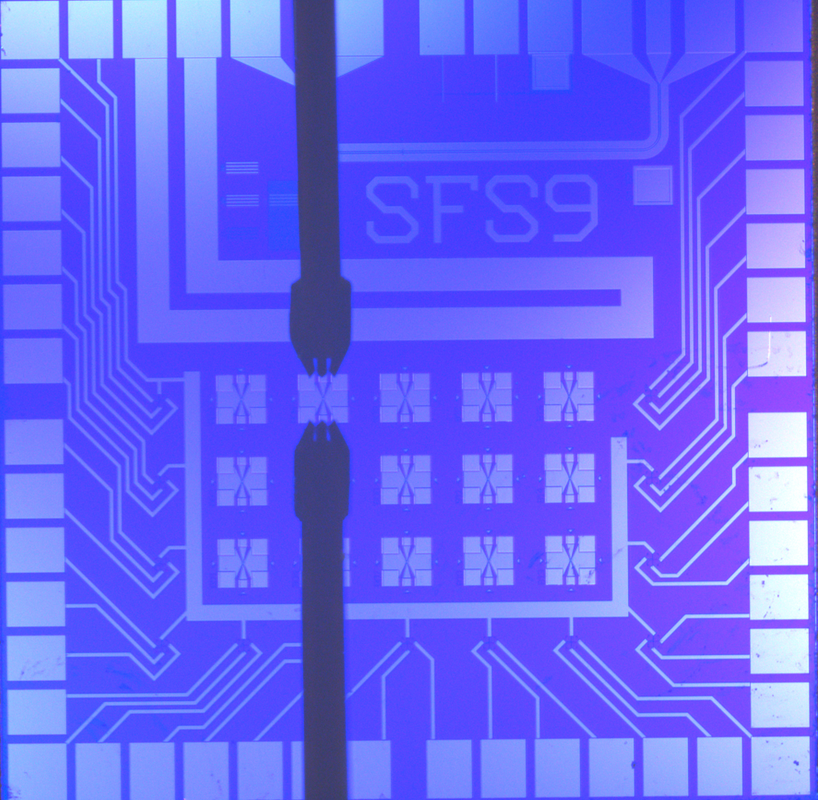
NIST’s artificial synapse, designed for neuromorphic computing, mimics the operation of switch between two neurons. One artificial synapse is located at the center of each X. This chip is 1 square centimeter in size. (The thick black vertical lines are electrical probes used for testing.) (credit: NIST)

A superconducting “synapse” that “learns” like a biological system, operating like the human brain, has been built by researchers at the National Institute of Standards and Technology (NIST).

The NIST switch, described in an open-access paper in Science Advances, provides a missing link for neuromorphic (brain-like) computers, according to the researchers. Such “non-von Neumann architecture” future computers could significantly speed up analysis and decision-making for applications such as self-driving cars and cancer diagnosis.

The research is supported by the Intelligence Advanced Research Projects Activity (IARPA) Cryogenic Computing Complexity Program, which was launched in 2014 with the goal of paving the way to “a new generation of superconducting supercomputer development beyond the exascale.”*

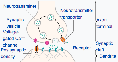
A synapse is a connection or switch between two neurons, controlling transmission of signals. (credit: NIST)

NIST’s artificial synapse is a metallic cylinder 10 micrometers in diameter — about 10 times larger than a biological synapse. It simulates a real synapse by processing incoming electrical spikes (pulsed current from a neuron) and customizing spiking output signals. The more firing between cells (or processors), the stronger the connection. That process enables both biological and artificial synapses to maintain old circuits and create new ones.

Dramatically faster, lower-energy-required, compared to human synapses

But the NIST synapse has two unique features that the researchers say are superior to human synapses and to other artificial synapses:

  • Operating at 100 GHz, it can fire at a rate that is much faster than the human brain — 1 billion times per second, compared to a brain cell’s rate of about 50 times per second.
  • It uses only about one ten-thousandth as much energy as a human synapse. The spiking energy is less than 1 attojoule** — roughly equivalent to the miniscule chemical energy bonding two atoms in a molecule — compared to the roughly 10 femtojoules (10,000 attojoules) per synaptic event in the human brain. Current neuromorphic platforms are orders of magnitude less efficient than the human brain. “We don’t know of any other artificial synapse that uses less energy,” NIST physicist Mike Schneider said.

Superconducting devices mimicking brain cells and transmission lines have been developed, but until now, efficient synapses — a crucial piece — have been missing. The new Josephson junction-based artificial synapse would be used in neuromorphic computers made of superconducting components (which can transmit electricity without resistance), so they would be more efficient than designs based on semiconductors or software. Data would be transmitted, processed, and stored in units of magnetic flux.

The brain is especially powerful for tasks like image recognition because it processes data both in sequence and simultaneously and it stores memories in synapses all over the system. A conventional computer processes data only in sequence and stores memory in a separate unit.

The new NIST artificial synapses combine small size, superfast spiking signals, and low energy needs, and could be stacked into dense 3D circuits for creating large systems. They could provide a unique route to a far more complex and energy-efficient neuromorphic system than has been demonstrated with other technologies, according to the researchers.

Nature News does raise some concerns about the research, quoting neuromorphic-technology experts: “Millions of synapses would be necessary before a system based on the technology could be used for complex computing; it remains to be seen whether it will be possible to scale it to this level. … The synapses can only operate at temperatures close to absolute zero, and need to be cooled with liquid helium. That this might make the chips impractical for use in small devices, although a large data centre might be able to maintain them. … We don’t yet understand enough about the key properties of the [biological] synapse to know how to use them effectively.”


Inside a superconducting synapse 

The NIST synapse is a customized Josephson junction***, long used in NIST voltage standards. These junctions are a sandwich of superconducting materials with an insulator as a filling. When an electrical current through the junction exceeds a level called the critical current, voltage spikes are produced.

Illustration showing the basic operation of NIST’s artificial synapse, based on a Josephson junction. Very weak electrical current pulses are used to control the number of nanoclusters (green) pointing in the same direction. Shown here: a “magnetically disordered state” (left) vs. “magnetically ordered state” (right). (credit: NIST)

Each artificial synapse uses standard niobium electrodes but has a unique filling made of nanoscale clusters (“nanoclusters”) of manganese in a silicon matrix. The nanoclusters — about 20,000 per square micrometer — act like tiny bar magnets with “spins” that can be oriented either randomly or in a coordinated manner. The number of nanoclusters pointing in the same direction can be controlled, which affects the superconducting properties of the junction.

Diagram of circuit used in the simulation. The blue and red areas represent pre- and post-synapse neurons, respectively. The X symbol represents the Josephson junction. (credit: Michael L. Schneider et al./Science Advances)

The synapse rests in a superconducting state, except when it’s activated by incoming current and starts producing voltage spikes. Researchers apply current pulses in a magnetic field to boost the magnetic ordering — that is, the number of nanoclusters pointing in the same direction.

This magnetic effect progressively reduces the critical current level, making it easier to create a normal conductor and produce voltage spikes. The critical current is the lowest when all the nanoclusters are aligned. The process is also reversible: Pulses are applied without a magnetic field to reduce the magnetic ordering and raise the critical current. This design, in which different inputs alter the spin alignment and resulting output signals, is similar to how the brain operates.

Synapse behavior can also be tuned by changing how the device is made and its operating temperature. By making the nanoclusters smaller, researchers can reduce the pulse energy needed to raise or lower the magnetic order of the device. Raising the operating temperature slightly from minus 271.15 degrees C (minus 456.07 degrees F) to minus 269.15 degrees C (minus 452.47 degrees F), for example, results in more and higher voltage spikes.


* Future exascale supercomputers would run at 1018 exaflops (“flops” = floating point operations per second) or more. The current fastest supercomputer — the Sunway TaihuLight — operates at about 0.1 exaflops; zettascale computers, the next step beyond exascale, would run 10,000 times faster than that.

** An attojoule is 10-18 joule, a unit of energy, and is one-thousandth of a femtojoule.

*** The Josephson effect is the phenomenon of supercurrent — i.e., a current that flows indefinitely long without any voltage applied — across a device known as a Josephson junction, which consists of two superconductors coupled by a weak link. — Wikipedia


Abstract of Ultralow power artificial synapses using nanotextured magnetic Josephson junctions

Neuromorphic computing promises to markedly improve the efficiency of certain computational tasks, such as perception and decision-making. Although software and specialized hardware implementations of neural networks have made tremendous accomplishments, both implementations are still many orders of magnitude less energy efficient than the human brain. We demonstrate a new form of artificial synapse based on dynamically reconfigurable superconducting Josephson junctions with magnetic nanoclusters in the barrier. The spiking energy per pulse varies with the magnetic configuration, but in our demonstration devices, the spiking energy is always less than 1 aJ. This compares very favorably with the roughly 10 fJ per synaptic event in the human brain. Each artificial synapse is composed of a Si barrier containing Mn nanoclusters with superconducting Nb electrodes. The critical current of each synapse junction, which is analogous to the synaptic weight, can be tuned using input voltage spikes that change the spin alignment of Mn nanoclusters. We demonstrate synaptic weight training with electrical pulses as small as 3 aJ. Further, the Josephson plasma frequencies of the devices, which determine the dynamical time scales, all exceed 100 GHz. These new artificial synapses provide a significant step toward a neuromorphic platform that is faster, more energy-efficient, and thus can attain far greater complexity than has been demonstrated with other technologies.

Cancer ‘vaccine’ eliminates all traces of cancer in mice

Effects of in situ vaccination with CpG and anti-OX40 agents. Left: Mice genetically engineered to spontaneously develop breast cancers in all 10 of their mammary pads were injected into the first arising tumor (black arrow) with either a vehicle (inactive fluid) (left) or with CpG and anti-OX40 (right). Pictures were taken on day 80. (credit: Idit Sagiv-Barfi et al./ Sci. Transl. Med.)

Injecting minute amounts of two immune-stimulating agents directly into solid tumors in mice was able to eliminate all traces of cancer in the animals — including distant, untreated metastases (spreading cancer locations), according to a study by Stanford University School of Medicine researchers.

The researchers believe this new “in situ vaccination” method could serve as a rapid and relatively inexpensive cancer therapy — one that is unlikely to cause the adverse side effects often seen with bodywide immune stimulation.

The  approach works for many different types of cancers, including those that arise spontaneously, the study found.

“When we use these two agents together, we see the elimination of tumors all over the body,” said Ronald Levy*, MD, professor of oncology and senior author of the study, which was published Jan. 31 in Science Translational Medicine. “This approach bypasses the need to identify tumor-specific immune targets and doesn’t require wholesale activation of the immune system or customization of a patient’s immune cells.”

Many current immunotherapy approaches have been successful, but they each have downsides — from difficult-to-handle side effects to high-cost and lengthy preparation or treatment times.** “Our approach uses a one-time application of very small amounts of two agents to stimulate the immune cells only within the tumor itself,” Levy said. “In the mice, we saw amazing, bodywide effects, including the elimination of tumors all over the animal.”

Cancer-destroying T cells that target other tumors in the body

Levy’s method reactivates cancer-specific T cells (a type of white blood cell) by injecting microgram (one-millionth of a gram) amounts of the two agents directly into the tumor site.*** Because the two agents are injected directly into the tumor, only T cells that have infiltrated the tumor are activated. In effect, these T cells are “prescreened” by the body to recognize only cancer-specific proteins.

Some of these tumor-specific, activated T cells then leave the original tumor to find and destroy other identical tumors throughout the body.


“I don’t think there’s a limit to the type of tumor we could potentially treat, as long as it has been infiltrated by the immune system.” — Ronald Levy, MD.


The approach worked “startlingly well” in laboratory mice with transplanted mouse lymphoma tumors in two sites on their bodies, the researchers say. Injecting one tumor site with the two agents caused the regression not just of the treated tumor, but also of the second, untreated tumor. In this way, 87 of 90 mice were cured of the cancer. Although the cancer recurred in three of the mice, the tumors again regressed after a second treatment. The researchers saw similar results in mice bearing breast, colon and melanoma tumors.

Mice genetically engineered to spontaneously develop breast cancers in all 10 of their mammary pads also responded to the treatment. Treating the first tumor that arose often prevented the occurrence of future tumors and significantly increased the animals’ life span, the researchers found.

Finally, researchers explored the specificity of the T cells. They transplanted two types of tumors into the mice. They transplanted the same lymphoma cancer cells in two locations, and transplanted a colon cancer cell line in a third location. Treatment of one of the lymphoma sites caused the regression of both lymphoma tumors but did not affect the growth of the colon cancer cells.

“This is a very targeted approach,” Levy said. “Only the tumor that shares the protein targets displayed by the treated site is affected. We’re attacking specific targets without having to identify exactly what proteins the T cells are recognizing.”

Lymphoma clinical trial

The current clinical trial is expected to recruit about 15 patients with low-grade lymphoma. If successful, Levy believes the treatment could be useful for many tumor types. He envisions a future in which clinicians inject the two agents into solid tumors in humans prior to surgical removal of the cancer. This would prevent recurrence of cancer due to unidentified metastases or lingering cancer cells, or even head off the development of future tumors that arise due to genetic mutations like BRCA1 and 2.

* Levy, who holds the Robert K. and Helen K. Summy Professorship in the School of Medicine, is also a member of the Stanford Cancer Institute and Stanford Bio-X. Levy is a pioneer in the field of cancer immunotherapy, in which researchers try to harness the immune system to combat cancer. Research in his laboratory formerly led to the development of rituximab, one of the first monoclonal antibodies approved for use as an anticancer treatment in humans. Professor of radiology Sanjiv Gambhir, MD, PhD, senior author of the paper, is the founder and equity holder in CellSight Inc., which develops and translates multimodality strategies to image cell trafficking and transplantation. The research was supported by the National Institutes of Health, the Leukemia and Lymphoma Society, the Boaz and Varda Dotan Foundation, and the Phil N. Allen Foundation. Stanford’s Department of Medicine also supported the work.

** Some immunotherapy approaches rely on stimulating the immune system throughout the body. Others target naturally occurring checkpoints that limit the anti-cancer activity of immune cells. Still others, like the CAR T-cell therapy recently approved to treat some types of leukemia and lymphomas, require a patient’s immune cells to be removed from the body and genetically engineered to attack the tumor cells. Immune cells like T cells recognize the abnormal proteins often present on cancer cells and infiltrate to attack the tumor. However, as the tumor grows, it often devises ways to suppress the activity of the T cells.

*** One agent, CpG, that induces an immune response in a short stretch of DNA called a CpG oligonucleotide, works with other nearby immune cells to amplify the expression of an activating receptor called OX40 on the surface of the T cells. The other agent, an antibody that binds to OX40, activates the T cells to lead the charge against the cancer cells.


Abstract of Eradication of spontaneous malignancy by local immunotherapy

It has recently become apparent that the immune system can cure cancer. In some of these strategies, the antigen targets are preidentified and therapies are custom-made against these targets. In others, antibodies are used to remove the brakes of the immune system, allowing preexisting T cells to attack cancer cells. We have used another noncustomized approach called in situ vaccination. Immunoenhancing agents are injected locally into one site of tumor, thereby triggering a T cell immune response locally that then attacks cancer throughout the body. We have used a screening strategy in which the same syngeneic tumor is implanted at two separate sites in the body. One tumor is then injected with the test agents, and the resulting immune response is detected by the regression of the distant, untreated tumor. Using this assay, the combination of unmethylated CG–enriched oligodeoxynucleotide (CpG)—a Toll-like receptor 9 (TLR9) ligand—and anti-OX40 antibody provided the most impressive results. TLRs are components of the innate immune system that recognize molecular patterns on pathogens. Low doses of CpG injected into a tumor induce the expression of OX40 on CD4+T cells in the microenvironment in mouse or human tumors. An agonistic anti-OX40 antibody can then trigger a T cell immune response, which is specific to the antigens of the injected tumor. Remarkably, this combination of a TLR ligand and an anti-OX40 antibody can cure multiple types of cancer and prevent spontaneous genetically driven cancers.

Penn researchers create first optical transistor comparable to an electronic transistor

By precisely controlling the mixing of optical signals, Ritesh Agarwal’s research team says they have taken an important step toward photonic (optical) computing. (credit: Sajal Dhara)

In an open-access paper published in Nature Communications, Ritesh Agarwal, a professor the University of Pennsylvania School of Engineering and Applied Science, and his colleagues say that they have made significant progress in photonic (optical) computing by creating a prototype of a working optical transistor with properties similar to those of a conventional electronic transistor.*

Optical transistors, using photons instead of electrons, promise to one day be more powerful than the electronic transistors currently used in computers.

Agarwal’s research on photonic computing has been focused on finding the right combination and physical configuration of nonlinear materials that can amplify and mix light waves in ways that are analogous to electronic transistors. “One of the hurdles in doing this with light is that materials that are able to mix optical signals also tend to have very strong background signals as well. That background signal would drastically reduce the contrast and on/off ratios leading to errors in the output,” Agarwal explained.

How the new optical transistor works

Schematic of a cadmium sulfide nanobelt device with source (S) and drain (D) electrodes. The fundamental wave at the frequency of ω, which is normally incident upon the belt, excites the second-harmonic (twice the frequency) wave at 2ω, which is back-scattered. (credit: Ming-Liang Ren et al./Nature Communications)

To address this issue, Agarwal’s research group started by creating a system with no disruptive optical background signal. To do that, they used a “nanobelt”* made out of cadmium sulfide. Then, by applying an electrical field across the nanobelt, the researchers were able to introduce optical nonlinearities (similar to the nonlinearities in electronic transistors), which enabled a signal mixing output that was otherwise zero.

“Our system turns on from zero to extremely large values,” Agarwal said.** “For the first time, we have an optical device with output that truly resembles an electronic transistor.”

The next steps toward a fully functioning photonic computer will involve integrating optical circuits with optical interconnects, modulators, and detectors to achieve actual on-chip integrated photonic computation.

The research was supported by the US Army Research Office and the National Science Foundation.

* “Made of semiconducting metal oxides, nanobelts are extremely thin and flat structures. They are chemically pure, structurally uniform, largely defect-free, with clean surfaces that do not require protection against oxidation. Each is made up of a single crystal with specific surface planes and shape.” — Reade International Corp.

** That is, the system was capable of precisely controlling the mixing of optical signals via controlled electric fields, with outputs with near-perfect contrast and extremely large on/off ratios. “Our study demonstrates a new way to dynamically control nonlinear optical signals in nanoscale materials with ultrahigh signal contrast and signal saturation, which can enable the development of nonlinear optical transistors and modulators for on-chip photonic devices with high-performance metrics and small-form factors, which can be further enhanced by integrating with nanoscale optical cavities,” the researchers note in the paper.


Abstract of Strong modulation of second-harmonic generation with very large contrast in semiconducting CdS via high-field domain

Dynamic control of nonlinear signals is critical for a wide variety of optoelectronic applications, such as signal processing for optical computing. However, controlling nonlinear optical signals with large modulation strengths and near-perfect contrast remains a challenging problem due to intrinsic second-order nonlinear coefficients via bulk or surface contributions. Here, via electrical control, we turn on and tune second-order nonlinear coefficients in semiconducting CdS nanobelts from zero to up to 151 pm V−1, a value higher than other intrinsic nonlinear coefficients in CdS. We also observe ultrahigh ON/OFF ratio of >104 and modulation strengths ~200% V−1 of the nonlinear signal. The unusual nonlinear behavior, including super-quadratic voltage and power dependence, is ascribed to the high-field domain, which can be further controlled by near-infrared optical excitation and electrical gating. The ability to electrically control nonlinear optical signals in nanostructures can enable optoelectronic devices such as optical transistors and modulators for on-chip integrated photonics.

The Princess Leia project: ‘volumetric’ 3D images that float in ‘thin air’

Inspired by the iconic Stars Wars scene with Princess Leia in distress, Brigham Young University engineers and physicists have created the “Princess Leia project” — a new technology for creating 3D “volumetric images” that float in the air and that you can walk all around and see from almost any angle.*

“Our group has a mission to take the 3D displays of science fiction and make them real,” said electrical and computer engineering professor and holography expert Daniel Smalley, lead author of a Jan. 25 Nature paper on the discovery.

The image of Princess Leia portrayed in the movie is actually not a hologram, he explains. A holographic display scatters light only on a 2D surface. So you have to be looking at a limited range of angles to see the image, which is also normally static. Instead, a moving volumetric display can be seen from any angle and you can even reach your hand into it. Examples include the 3D displays Tony Stark interacts with in Ironman and the massive image-projecting table in Avatar.*

How to create a 3D volumetric image from a single moving particle

BYU student Erich Nygaard, depicted as a moving 3D image, mimicks the Princess Leia projection in the iconic Star Wars scene (“Help me Obi Wan Kenobi, you’re my only hope”). (credit: Dan Smalley Lab)

The team’s free-space volumetric display technology, called “Optical Trap Display,” is based on photophoretic** optical trapping (controlled by a laser beam) of a rapidly moving particle (of a plant fiber called cellulose in this case). This technique takes advantage of human persistence of vision (at more than 10 images per second we don’t see a moving point of light, just the pattern it traces in space — the same phenomenon that makes movies and video work).

As the laser beam moves the trapped particle around, three more laser beams illuminate the particle with RGB (red-green-blue) light. The resulting fast-moving dot traces out a color image in three dimensions (you can see the vertical scan lines in one vertical slice in the Princess Leia image above) — producing a full-color, volumetric (3D) still image in air with 10-micrometer resolution, which allows for fine detail. The technology also features low noticeable speckle (the annoying specks seen in holograms).***

Applications in the real (and virtual) world

So far, Smalley and his student researchers have 3D light-printed a butterfly, a prism, the stretch-Y BYU logo, rings that wrap around an arm, and an individual in a lab coat crouched in a position similar to Princess Leia as she begins her projected message. The images in this proof-of-concept prototype are still in the range of millimeters. But in the Nature paper, the researchers say they anticipate that the device “can readily be scaled using parallelism and [they] consider this platform to be a viable method for creating 3D images that share the same space as the user, as physical objects would.”

What about augmented and virtual-reality uses? “While I think this technology is not really AR or VR but just ‘R,’  there are a lot of interesting ways volumetric images can enhance and augment the world around us,” Smalley told KurzweilAI in an email. “A very-near-term application could be the use of levitated particles as ‘streamers’ to show the expected flow of air over actual physical objects. That is, instead of looking at a computer screen to see fluid flow over a turbine blade, you could set a volumetric projector next to the actual turbine blade and see particles form ribbons to shown expected fluid flow juxtaposed on the real object.

“In a scaled-up version of the display, a projector could place a superimposed image of a part on an engine showing a technician the exact location and orientation of that part. An even more refined version could create a magic portal in your home where you could see the size of shoes you just ordered and set your foot inside to (visually) check the fit. Other applications would included sparse telepresence, satellite tracking, command and control surveillance, surgical planning, tissue tagging, catheter guidance and other medical visualization applications.”

How soon? “I won’t make a prediction on exact timing but if we make as much progress in the next four years as we did in the last four years (a big ‘if’), then we would have a display of usable size by the end of that period. We have had a number of interested parties from a variety of fields. We are open to an exclusive agreement, given the right partner.”

* Smalley says he has long dreamed of building the kind of 3D holograms that pepper science-fiction films. But watching inventor Tony Stark thrust his hands through ghostly 3D body armor in the 2008 film Iron Man, Smalley realized that he could never achieve that using holography, the current standard for high-tech 3D display, because Stark’s hand would block the hologram’s light source. “That irritated me,” he says. He immediately tried to work out how to get around that.

** “Photophoresis denotes the phenomenon that small particles suspended in gas (aerosols) or liquids (hydrocolloids) start to migrate when illuminated by a sufficiently intense beam of light.” — Wikipedia

*** Previous researchers have created volumetric imagery, but the Smalley team says it’s the first to use optical trapping and color effectively. “Among volumetric systems, we are aware of only three such displays that have been successfully demonstrated in free space: induced plasma displays, modified air displays, and acoustic levitation displays. Plasma displays have yet to demonstrate RGB color or occlusion in free space. Modified air displays and acoustic levitation displays rely on mechanisms that are too coarse or too inertial to compete directly with holography at present.” — D.E. Smalley et al./Nature


Nature video | Pictures in the air: 3D printing with light


Abstract of A photophoretic-trap volumetric display

Free-space volumetric displays, or displays that create luminous image points in space, are the technology that most closely resembles the three-dimensional displays of popular fiction. Such displays are capable of producing images in ‘thin air’ that are visible from almost any direction and are not subject to clipping. Clipping restricts the utility of all three-dimensional displays that modulate light at a two-dimensional surface with an edge boundary; these include holographic displays, nanophotonic arrays, plasmonic displays, lenticular or lenslet displays and all technologies in which the light scattering surface and the image point are physically separate. Here we present a free-space volumetric display based on photophoretic optical trapping that produces full-colour graphics in free space with ten-micrometre image points using persistence of vision. This display works by first isolating a cellulose particle in a photophoretic trap created by spherical and astigmatic aberrations. The trap and particle are then scanned through a display volume while being illuminated with red, green and blue light. The result is a three-dimensional image in free space with a large colour gamut, fine detail and low apparent speckle. This platform, named the Optical Trap Display, is capable of producing image geometries that are currently unobtainable with holographic and light-field technologies, such as long-throw projections, tall sandtables and ‘wrap-around’ displays.

MIT nanosystem delivers precise amounts of drugs directly to a tiny spot in the brain

MIT’s miniaturized system can deliver multiple drugs to precise locations in the brain, also monitor and control neural activity (credit: MIT)

MIT researchers have developed a miniaturized system that can deliver tiny quantities of medicine to targeted brain regions as small as 1 cubic millimeter, with precise control over how much drug is given. The goal is to treat diseases that affect specific brain circuits without interfering with the normal functions of the rest of the brain.*

“We believe this tiny microfabricated device could have tremendous impact in understanding brain diseases, as well as providing new ways of delivering biopharmaceuticals and performing biosensing in the brain,” says Robert Langer, the David H. Koch Institute Professor at MIT and one of the senior authors of an open-access paper that appears in the Jan. 24 issue of Science Translational Medicine.**

Miniaturized neural drug delivery system (MiNDS). Top: Miniaturized delivery needle with multiple fluidic channels for delivering different drugs. Bottom: scanning electron microscope image of cannula tip for delivering a drug or optogenetic light (to stimulate neurons) and a tungsten electrode (yellow dotted area — magnified view in inset) for detecting neural activity. (credit: Dagdeviren et al., Sci. Transl. Med., adapted by KurzweilAI)

The researchers used state-of-the-art microfabrication techniques to construct cannulas (thin tubes) with diameters of about 30 micrometers (width of a fine human hair) and lengths up to 10 centimeters. These cannulas are contained within a stainless steel needle with a diameter of about 150 micrometers. Inside the cannulas are small pumps that can deliver tiny doses (hundreds of nanoliters***) deep into the brains of rats — with very precise control over how much drug is given and where it goes.

In one experiment, they delivered a drug called muscimol to a rat brain region called the substantia nigra, which is located deep within the brain and helps to control movement. Previous studies have shown that muscimol induces symptoms similar to those seen in Parkinson’s disease. The researchers were able to stimulate the rats to continually turn in a clockwise direction. They also could also halt the Parkinsonian behavior by delivering a dose of saline through a different channel to wash the drug away.

“Since the device can be customizable, in the future we can have different channels for different chemicals, or for light, to target tumors or neurological disorders such as Parkinson’s disease or Alzheimer’s,” says Canan Dagdeviren, the LG Electronics Career Development Assistant Professor of Media Arts and Sciences and the lead author of the paper.

This device could also make it easier to deliver potential new treatments for behavioral neurological disorders such as addiction or obsessive compulsive disorder. (These may be caused by specific disruptions in how different parts of the brain communicate with each other.)

Measuring drug response

The researchers also showed that they could incorporate an electrode into the tip of the cannula, which can be used to monitor how neurons’ electrical activity changes after drug treatment. They are now working on adapting the device so it can also be used to measure chemical or mechanical changes that occur in the brain following drug treatment.

The cannulas can be fabricated in nearly any length or thickness, making it possible to adapt them for use in brains of different sizes, including the human brain, the researchers say.

“This study provides proof-of-concept experiments, in large animal models, that a small, miniaturized device can be safely implanted in the brain and provide miniaturized control of the electrical activity and function of single neurons or small groups of neurons. The impact of this could be significant in focal diseases of the brain, such as Parkinson’s disease,” says Antonio Chiocca, neurosurgeon-in-chief and chairman of the Department of Neurosurgery at Brigham and Women’s Hospital, who was not involved in the research.

The research was funded by the National Institutes of Health and the National Institute of Biomedical Imaging and Bioengineering.

* To treat brain disorders, drugs (such as l-dopa, a dopamine precursor used to treat Parkinson’s disease, and Prozac, used to boost serotonin levels in patients with depression) often interact with brain chemicals called neurotransmitters (or the cell receptors interact with neurotransmitters) — creating side effects throughout the brain.

** Michael Cima, the David H. Koch Professor of Engineering in the Department of Materials Science and Engineering and a member of MIT’s Koch Institute for Integrative Cancer Research, is also a senior author of the paper.

*** It would take one billion nanoliter drops to fill 4 cups.


Abstract of Miniaturized neural system for chronic, local intracerebral drug delivery

Recent advances in medications for neurodegenerative disorders are expanding opportunities for improving the debilitating symptoms suffered by patients. Existing pharmacologic treatments, however, often rely on systemic drug administration, which result in broad drug distribution and consequent increased risk for toxicity. Given that many key neural circuitries have sub–cubic millimeter volumes and cell-specific characteristics, small-volume drug administration into affected brain areas with minimal diffusion and leakage is essential. We report the development of an implantable, remotely controllable, miniaturized neural drug delivery system permitting dynamic adjustment of therapy with pinpoint spatial accuracy. We demonstrate that this device can chemically modulate local neuronal activity in small (rodent) and large (nonhuman primate) animal models, while simultaneously allowing the recording of neural activity to enable feedback control.

The Doomsday Clock is now two minutes before midnight

(credit: Bulletin of the Atomic Scientists)

Citing growing nuclear risks and unchecked climate dangers, the Doomsday Clock — the symbolic point of annihilation — is now two minutes to midnight, the closest the Clock has been since 1953 at the height of the Cold War, according to a statement today (Jan. 25) by the Bulletin of the Atomic Scientists.

“In 2017, world leaders failed to respond effectively to the looming threats of nuclear war and climate change, making the world security situation more dangerous than it was a year ago — and as dangerous as it has been since World War II,” according to the Atomic Scientists’ Science and Security Board in consultation with the Board of Sponsors, which includes 15 Nobel Laureates.


“This is a dangerous time, but the danger is of our own making. Humankind has invented the implements of apocalypse; so can it invent the methods of controlling and eventually eliminating them. This year, leaders and citizens of the world can move the Doomsday Clock and the world away from the metaphorical midnight of global catastrophe by taking common-sense action.” — Lawrence Krauss, director of the Origins Project at Arizona State University, Foundation Professor at School of Earth and Space Exploration and Physics Department, Arizona State University, and chair, Bulletin of the Atomic Scientists’ Board of Sponsors.


The increased risks driving the decision to move the clock include:

Nuclear. Hyperbolic rhetoric and provocative actions from North Korea and the U.S. have increased the possibility of nuclear war by accident or miscalculation. These include U.S.-Russian military entanglements, South China Sea tensions, escalating rhetoric between Pakistan and India,  uncertainty about continued U.S. support for the Iran nuclear deal.

Decline of U.S. leadership and a related demise of diplomacy under the Trump Administration. “In 2017, the United States backed away from its longstanding leadership role in the world, reducing its commitment to seek common ground and undermining the overall effort toward solving pressing global governance challenges. Neither allies nor adversaries have been able to reliably predict U.S. actions or understand when U.S. pronouncements are real and when they are mere rhetoric. International diplomacy has been reduced to name-calling, giving it a surrealistic sense of unreality that makes the world security situation ever more threatening.”

Climate change. “The nations of the world will have to significantly decrease their greenhouse gas emissions to keep climate risks manageable, and so far, the global response has fallen far short of meeting this challenge.”

How to #RewindtheDoomsdayClock

According to Bulletin of the Atomic Scientists:

* U.S. President Donald Trump should refrain from provocative rhetoric regarding North Korea, recognizing the impossibility of predicting North Korean reactions. The U.S. and North Korean governments should open multiple channels of communication.

* The world community should pursue, as a short-term goal, the cessation of North Korea’s nuclear weapon and ballistic missile tests. North Korea is the only country to violate the norm against nuclear testing in 20 years.

* The Trump administration should abide by the terms of the Joint Comprehensive Plan of Action for Iran’s nuclear program unless credible evidence emerges that Iran is not complying with the agreement or Iran agrees to an alternative approach that meets U.S. national security needs.

* The United States and Russia should discuss and adopt measures to prevent peacetime military incidents along the borders of NATO.

* U.S. and Russian leaders should return to the negotiating table to resolve differences over the INF treaty, to seek further reductions in nuclear arms, to discuss a lowering of the alert status of the nuclear arsenals of both countries, to limit nuclear modernization programs that threaten to create a new nuclear arms race, and to ensure that new tactical or low-yield nuclear weapons are not built, and existing tactical weapons are never used on the battlefield.

* U.S. citizens should demand, in all legal ways, climate action from their government. Climate change is a real and serious threat to humanity.

* Governments around the world should redouble their efforts to reduce greenhouse gas emissions so they go well beyond the initial, inadequate pledges under the Paris Agreement.

* The international community should establish new protocols to discourage and penalize the misuse of information technology to undermine public trust in political institutions, in the media, in science, and in the existence of objective reality itself.

Worldwide deployments of nuclear weapons, 2017

“As of mid-2017, there are nearly 15,000 nuclear weapons in the world, located at some 107 sites in 14 countries. Roughly, 9400 of these weapons are in military arsenals; the remaining weapons are retired and awaiting dismantlement. Nearly 4000 are operationally available, and some 1800 are on high alert and ready for use on short notice.

“By far, the largest concentrations of nuclear weapons reside in Russia and the United States, which possess 93 percent of the total global inventory. In addition to the seven other countries with nuclear weapon stockpiles (Britain, France, China, Israel, India, Pakistan, and North Korea), five nonnuclear NATO allies (Belgium, Germany, Italy, the Netherlands, and Turkey) host about 150 US nuclear bombs at six air bases.”

Hans M. Kristensen & Robert S. Norris, Worldwide deployments of nuclear weapons, Bulletin of the Atomic Scientists 2017. Pages 289-297 | Published online: 31 Aug 2017.

Ultra-thin ‘atomistor’ synapse-like memory storage device paves way for faster, smaller, smarter computer chips

Illustration of single-atom-layer “atomristors” — the thinnest-ever memory-storage device (credit: Cockrell School of Engineering, The University of Texas at Austin)

A team of electrical engineers at The University of Texas at Austin and scientists at Peking University has developed a one-atom-thick 2D “atomristor” memory storage device that may lead to faster, smaller, smarter computer chips.

The atomristor (atomic memristor) improves upon memristor (memory resistor) memory storage technology by using atomically thin nanomaterials (atomic sheets). (Combining memory and logic functions, similar to the synapses of biological brains, memristors “remember” their previous state after being turned off.)

Schematic of atomristor memory sandwich based on molybdenum sulfide (MoS2) in a form of a single-layer atomic sheet grown on gold foil. (Blue: Mo; yellow: S) (credit: Ruijing Ge et al./Nano Letters)

Memory storage and transistors have, to date, been separate components on a microchip. Atomristors combine both functions on a single, more-efficient device. They use metallic atomic sheets (such as graphene or gold) as electrodes and semiconducting atomic sheets (such as molybdenum sulfide) as the active layer. The entire memory cell is a two-layer sandwich only ~1.5 nanometers thick.

“The sheer density of memory storage that can be made possible by layering these synthetic atomic sheets onto each other, coupled with integrated transistor design, means we can potentially make computers that learn and remember the same way our brains do,” said Deji Akinwande, associate professor in the Cockrell School of Engineering’s Department of Electrical and Computer Engineering.

“This discovery has real commercialization value, as it won’t disrupt existing technologies,” Akinwande said. “Rather, it has been designed to complement and integrate with the silicon chips already in use in modern tech devices.”

The research is described in an open-access paper in the January American Chemical Society journal Nano Letters.

Longer battery life in cell phones

For nonvolatile operation (preserving data after power is turned off), the new design also “offers a substantial advantage over conventional flash memory, which occupies far larger space. In addition, the thinness allows for faster and more efficient electric current flow,” the researchers note in the paper.

The research team also discovered another unique application for the atomristor technology: Atomristors are the smallest radio-frequency (RF) memory switches to be demonstrated, with no DC battery consumption, which could ultimately lead to longer battery life for cell phones and other battery-powered devices.*

Funding for the UT Austin team’s work was provided by the National Science Foundation and the Presidential Early Career Award for Scientists and Engineers, awarded to Akinwande in 2015.

* “Contemporary switches are realized with transistor or microelectromechanical devices, both of which are volatile, with the latter also requiring large switching voltages [which are not ideal] for mobile technologies,” the researchers note in the paper. Atomristors instead allow for nonvolatile low-power radio-frequency (RF) switches with “low voltage operation, small form-factor, fast switching speed, and low-temperature integration compatible with silicon or flexible substrates.”


Abstract of Atomristor: Nonvolatile Resistance Switching in Atomic Sheets of Transition Metal Dichalcogenides

Recently, two-dimensional (2D) atomic sheets have inspired new ideas in nanoscience including topologically protected charge transport,1,2 spatially separated excitons,3 and strongly anisotropic heat transport.4 Here, we report the intriguing observation of stable nonvolatile resistance switching (NVRS) in single-layer atomic sheets sandwiched between metal electrodes. NVRS is observed in the prototypical semiconducting (MX2, M = Mo, W; and X = S, Se) transitional metal dichalcogenides (TMDs),5 which alludes to the universality of this phenomenon in TMD monolayers and offers forming-free switching. This observation of NVRS phenomenon, widely attributed to ionic diffusion, filament, and interfacial redox in bulk oxides and electrolytes,6−9 inspires new studies on defects, ion transport, and energetics at the sharp interfaces between atomically thin sheets and conducting electrodes. Our findings overturn the contemporary thinking that nonvolatile switching is not scalable to subnanometre owing to leakage currents.10 Emerging device concepts in nonvolatile flexible memory fabrics, and brain-inspired (neuromorphic) computing could benefit substantially from the wide 2D materials design space. A new major application, zero-static power radio frequency (RF) switching, is demonstrated with a monolayer switch operating to 50 GHz.

An artificial synapse for future miniaturized portable ‘brain-on-a-chip’ devices

Biological synapse structure (credit: Thomas Splettstoesser/CC)

MIT engineers have designed a new artificial synapse made from silicon germanium that can precisely control the strength of an electric current flowing across it.

In simulations, the researchers found that the chip and its synapses could be used to recognize samples of handwriting with 95 percent accuracy. The engineers say the new design, published today (Jan. 22) in the journal Nature Materials, is a major step toward building portable, low-power neuromorphic chips for use in pattern recognition and other machine-learning tasks.

Controlling the flow of ions: the challenge

Researchers in the emerging field of “neuromorphic computing” have attempted to design computer chips that work like the human brain. The idea is to apply a voltage across layers that would cause ions (electrically charged atoms) to move in a switching medium (synapse-like space) to create conductive filaments in a manner that’s similar to how the “weight” (connection strength) of a synapse changes.

There are more than 100 trillion synapses (in a typical human brain) that mediate neuron signaling in the brain, strengthening some neural connections while pruning (weakening) others — a process that enables the brain to recognize patterns, remember facts, and carry out other learning tasks, all at lightning speeds.

Instead of carrying out computations based on binary, on/off signaling, like current digital chips, the elements of a “brain on a chip” would work in an analog fashion, exchanging a gradient of signals, or “weights” — much like neurons that activate in various ways (depending on the type and number of ions that flow across a synapse).

But it’s been difficult to control the flow of ions in existing synapse designs. These have multiple paths that make it difficult to predict where ions will make it through, according to research team leader Jeehwan Kim, PhD, an assistant professor in the departments of Mechanical Engineering and Materials Science and Engineering, a principal investigator in MIT’s Research Laboratory of Electronics and Microsystems Technology Laboratories.

“Once you apply some voltage to represent some data with your artificial neuron, you have to erase and be able to write it again in the exact same way,” Kim says. “But in an amorphous solid, when you write again, the ions go in different directions because there are lots of defects. This stream is changing, and it’s hard to control. That’s the biggest problem — nonuniformity of the artificial synapse.”

Epitaxial random access memory (epiRAM)

(Left) Cross-sectional transmission electron microscope image of 60 nm silicon-germanium (SiGe) crystal grown on a silicon substrate (diagonal white lines represent candidate dislocations). Scale bar: 25 nm. (Right) Cross-sectional scanning electron microscope image of an epiRAM device with titanium (Ti)–gold (Au) and silver (Ag)–palladium (Pd) layers. Scale bar: 100 nm. (credit: Shinhyun Choi et al./Nature Materials)

So instead of using amorphous materials as an artificial synapse, Kim and his colleagues created an new “epitaxial random access memory” (epiRAM) design.

They started with a wafer of silicon. They then grew a similar pattern of silicon germanium — a material used commonly in transistors — on top of the silicon wafer. Silicon germanium’s lattice is slightly larger than that of silicon, and Kim found that together, the two perfectly mismatched materials could form a funnel-like dislocation, creating a single path through which ions can predictably flow.*

This is the most uniform device we could achieve, which is the key to demonstrating artificial neural networks,” Kim says.

Testing the ability to recognize samples of handwriting

As a test, Kim and his team explored how the epiRAM device would perform if it were to carry out an actual learning task: recognizing samples of handwriting — which researchers consider to be a practical test for neuromorphic chips. Such chips would consist of artificial “neurons” connected to other “neurons” via filament-based artificial “synapses.”

Image-recognition simulation. (Left) A 3-layer multilayer-perception neural network with black and white input signal for each layer in algorithm level. The inner product (summation) of input neuron signal vector and first synapse array vector is transferred after activation and binarization as input vectors of second synapse arrays. (Right) Circuit block diagram of hardware implementation showing a synapse layer composed of epiRAM crossbar arrays and the peripheral circuit. (credit: Shinhyun Choi et al./Nature Materials)

They ran a computer simulation of an artificial neural network consisting of three sheets of neural layers connected via two layers of artificial synapses, based on measurements from their actual neuromorphic chip. They fed into their simulation tens of thousands of samples from the MNIST handwritten recognition dataset**, commonly used by neuromorphic designers.

They found that their neural network device recognized handwritten samples 95.1 percent of the time — close to the 97 percent accuracy of existing software algorithms running on large computers.

A chip to replace a supercomputer

The team is now in the process of fabricating a real working neuromorphic chip that can carry out handwriting-recognition tasks. Looking beyond handwriting, Kim says the team’s artificial synapse design will enable much smaller, portable neural network devices that can perform complex computations that are currently only possible with large supercomputers.

“Ultimately, we want a chip as big as a fingernail to replace one big supercomputer,” Kim says. “This opens a stepping stone to produce real artificial intelligence hardware.”

This research was supported in part by the National Science Foundation. Co-authors included researchers at Arizona State University.

* They applied voltage to each synapse and found that all synapses exhibited about the same current, or flow of ions, with about a 4 percent variation between synapses — a much more uniform performance compared with synapses made from amorphous material. They also tested a single synapse over multiple trials, applying the same voltage over 700 cycles, and found the synapse exhibited the same current, with just 1 percent variation from cycle to cycle.

** The MNIST (Modified National Institute of Standards and Technology database) is a large database of handwritten digits that is commonly used for training various image processing systems and for training and testing in the field of machine learning. It contains 60,000 training images and 10,000 testing images. 


Abstract of SiGe epitaxial memory for neuromorphic computing with reproducible high performance based on engineered dislocations

Although several types of architecture combining memory cells and transistors have been used to demonstrate artificial synaptic arrays, they usually present limited scalability and high power consumption. Transistor-free analog switching devices may overcome these limitations, yet the typical switching process they rely on—formation of filaments in an amorphous medium—is not easily controlled and hence hampers the spatial and temporal reproducibility of the performance. Here, we demonstrate analog resistive switching devices that possess desired characteristics for neuromorphic computing networks with minimal performance variations using a single-crystalline SiGe layer epitaxially grown on Si as a switching medium. Such epitaxial random access memories utilize threading dislocations in SiGe to confine metal filaments in a defined, one-dimensional channel. This confinement results in drastically enhanced switching uniformity and long retention/high endurance with a high analog on/off ratio. Simulations using the MNIST handwritten recognition data set prove that epitaxial random access memories can operate with an online learning accuracy of 95.1%.