New inventions track greenhouse gas, remediate oil spills

Camera test at Foljesjon, a lake in a research area west of Vanersborg, Sweden (credit: Linkoping University)

A new camera that can image methane in the air, allowing for precision monitoring of a greenhouse gas, has been developed by a team of researchers from Linköping and Stockholm Universities.

The new camera should help us better understand the rapid but irregular increase of methane in the atmosphere (which has puzzled researchers) and identify the sources and sinks of methane in the landscape. It may also suggest ways to reduce emissions.

”The camera is very sensitive, which means that the methane is both visible and measureable close to ground level, with much higher resolution [less than a square meter and at ambient levels (~1.8 ppmv, or parts per million volume)] than previously. Being able to measure on a small scale is crucial,” says Magnus Gålfalk, Assistant Professor at Tema Environmental Change, Linköping University who led the study.

An image of methane gas from the hyperspectral infrared camera, visualized in purple (credit: Linköping University)

The advanced hyperspectral (across the spectrum) thermal infrared camera weighs 30 kilos and measures 50 x 45 x 25 centimeters. It is optimized to measure the same portion of the solar radiation spectrum that methane absorbs and which makes methane such a powerful greenhouse gas.

The camera can be used to measure emissions from many environments including sewage sludge deposits, combustion processes, animal husbandry, and lakes.

For each pixel in the image (320 x 256 pixels), the camera records a precise spectrum range (in the 7.7 microns thermal IR region), which makes it possible to quantify the methane separately from the other gases.

The camera was developed by a team with expertise in astronomy, biogeochemistry, engineering. and environmental sciences. “We’re working to make it airborne for more large-scale methane mapping,” says principal investigator David Bastviken, professor at Tema Environmental Change, Linköping University.

The research was recently published in Nature Climate Change.

Super-absorbent material to soak up oil spills

Boron nitride material supported by a plant spike, demonstrating its light weight (credit: Weiwei Lei et al./Nature Communications)

In hopes of limiting the disastrous environmental effects of massive oil spills, materials scientists from Drexel University and Deakin University (Australia) have teamed up to manufacture and test a new “boron nitride nanosheet” material that can absorb oils and organic solvents up to 33 times its weight. That could make it possible to quickly mitigate these costly, environmentally damaging accidents.

The material, which literally absorbs oil like a sponge, is now ready to be tested by industry after two years of refinement in the laboratory at Deakin’s Institute for Frontier Materials (IFM).

Deakin Professor Ying (Ian) Chen, PhD, the lead author of the project’s research paper, recently published in Nature Communications, said the material is the most exciting advancement in oil spill remediation technology in decades.

“Oil spills are a global problem and wreak havoc on our aquatic ecosystems, not to mention they cost billions of dollars in damage,” Chen said. “Everyone remembers the Gulf Coast disaster, but here in Australia they are a regular problem, and not just in our waters. Oil spills from trucks and other vehicles can close freeways for an entire day, again amounting to large economic losses,” Chen said.

The nanosheet is made up of flakes just several nanometers (one billionth of a meter) in thickness with tiny holes. This strecture enables the nanosheet to increase its effective surface area to 273 square meters (3000 square feet) per gram.

Researchers from Drexel’s College of Engineering helped to study and functionalize the material, which started as boron nitride powder, commonly called “white graphite.” By forming the powder into atomically thin sheets, the material could be made into a sponge.

“The mechanochemical technique developed meant it was possible to produce high-concentration stable aqueous colloidal solutions of boron nitride sheets, which could then be transformed into the ultralight porous aerogels and membranes for oil clean-up,” said Vadym Mochalin, PhD, a co-author of the paper, who was a research associate professor at Drexel while working on the project, and is now an associate professor at Missouri University of Science and Technology.

The Drexel team used computational modeling to help understand the intimate details of how the material was formed. In the process, the team learned that the boron nitride nanosheets are flame resistant — which means they could also find applications in electrical and heat insulation.

The nanotechnology team at Deakin’s Institute for Frontier Materials has been working on boron nitride nanomaterials for two decades and has been internationally recognized for its work in the development of boron nitride nanotubes and nanosheets. This project is the next step in the IFM’s continued research to discover new uses for the material.


Abstract of Making methane visible

Methane (CH4) is one of the most important greenhouse gases, and an important energy carrier in biogas and natural gas. Its large-scale emission patterns have been unpredictable and the source and sink distributions are poorly constrained. Remote assessment of CH4 with high sensitivity at a m2 spatial resolution would allow detailed mapping of the near-ground distribution and anthropogenic sources in landscapes but has hitherto not been possible. Here we show that CH4 gradients can be imaged on the <m2scale at ambient levels (~1.8 ppm) and filmed using optimized infrared (IR) hyperspectral imaging. Our approach allows both spectroscopic confirmation and quantification for all pixels in an imaged scene simultaneously. It also has the ability to map fluxes for dynamic scenes. This approach to mapping boundary layer CH4 offers a unique potential way to improve knowledge about greenhouse gases in landscapes and a step towards resolving source–sink attribution and scaling issues.


Abstract of Boron nitride colloidal solutions, ultralight aerogels and freestanding membranes through one-step exfoliation and functionalization

Manufacturing of aerogels and membranes from hexagonal boron nitride (h-BN) is much more difficult than from graphene or graphene oxides because of the poor dispersibility of h-BN in water, which limits its exfoliation and preparation of colloidal solutions. Here, a simple, one-step mechano-chemical process to exfoliate and functionalize h-BN into highly water-dispersible, few-layer h-BN containing amino groups is presented. The colloidal solutions of few-layer h-BN can have unprecedentedly high concentrations, up to 30 mg ml−1, and are stable for up to several months. They can be used to produce ultralight aerogels with a density of 1.4 mg cm−3, which is ~1,500 times less than bulk h-BN, and freestanding membranes simply by cryodrying and filtration, respectively. The material shows strong blue light emission under ultraviolet excitation, in both dispersed and dry state.

‘Invisible wires’ could improve solar-cell efficiency

Silicon pillars emerge from nanosize holes in a thin gold film. The pillars funnel 97 percent of incoming light to a silicon substrate, a technology that could significantly boost the performance of conventional solar cells. (credit: Vijay Narasimhan, Stanford University)

Stanford scientists have discovered how to make the electrical wiring on top of solar cells nearly invisible to incoming light, using nanosize silicon pillars to hide the wires. The new design could dramatically boost solar-cell efficiency, the researchers suggest.

A solar cell is basically a semiconductor that converts sunlight into electricity, sandwiched between metal contacts that carry the electrical current generated by the cell. But with current designs, the shiny metal wires on top of the cell reflect sunlight away from the semiconductor surface, reducing the cell’s efficiency.

Now Stanford scientists have discovered how to hide the reflective upper contacts, funneling light directly to the semiconductor below by using silicon pillars to redirect the sunlight before it hits the metallic surface.


Stanford University | “Invisible wires” could boost solar-cell efficiency

Besides gold, the nanopillar architecture will  also work with contacts made of silver, platinum, nickel and other metals. In addition to silicon, this new technology can be used with other semiconducting materials for a variety of applications, including photosensors, light-emitting diodes and displays and transparent batteries, as well as solar cells.

The new method aims to improve on a wide variety of methods that have been reported by KurzweilAI.

The findings are published in the journal ACS Nano.


Abstract of Hybrid Metal–Semiconductor Nanostructure for Ultrahigh Optical Absorption and Low Electrical Resistance at Optoelectronic Interfaces

Engineered optoelectronic surfaces must control both the flow of light and the flow of electrons at an interface; however, nanostructures for photon and electron management have typically been studied and optimized separately. In this work, we unify these concepts in a new hybrid metal–semiconductor surface that offers both strong light absorption and high electrical conductivity. We use metal-assisted chemical etching to nanostructure the surface of a silicon wafer, creating an array of silicon nanopillars protruding through holes in a gold film. When coated with a silicon nitride anti-reflection layer, we observe broad-band absorption of up to 97% in this structure, which is remarkable considering that metal covers 60% of the top surface. We use optical simulations to show that Mie-like resonances in the nanopillars funnel light around the metal layer and into the substrate, rendering the metal nearly transparent to the incoming light. Our results show that, across a wide parameter space, hybrid metal–semiconductor surfaces with absorption above 90% and sheet resistance below 20 Ω/□ are realizable, suggesting a new paradigm wherein transparent electrodes and photon management textures are designed and fabricated together to create high-performance optoelectronic interfaces.

Capturing a single photon

Capturing a single photon from a pulse of light (credit: Weizmann Institute of Science)

Weizmann Institute of Science researchers have managed to isolate a single photon out of a pulse of light. Single photons may be the backbone of future quantum communication systems, the researchers say.

The mechanism relies on a physical effect that they call “single-photon Raman interaction” (SPRINT). “The advantage of SPRINT is that it is completely passive; it does not require any control fields — just the interaction between the atom and the optical pulse,” said Barak Dayan, PhD, head of the Weizmann Institute Quantum Optics group.

The experimental setup involves laser cooling and trapping of atoms (in this case, rubidium), optical nanofibers, and fabrication of chip-based, ultrahigh-quality glass microspheres.

Previously, a low-reflectivity beam splitter directing a small fraction of the incoming light toward a detector was used, with low success rates.

“The ability to divert a single photon from a flow could be harnessed for various tasks, from creating nonclassical states of light that are useful for basic scientific research, through eavesdropping on imperfect quantum-cryptography systems that rely on single photons, to increasing the security of your own quantum-communication systems,” Dayan said.

The findings of this research appeared Nov. 23, 2015 in Nature Photonics.


Abstract of Extraction of a single photon from an optical pulse

Removing a single photon from a pulse is one of the most elementary operations that can be performed on light, having both fundamental significance and practical applications in quantum communication and computation. So far, photon subtraction, in which the removed photon is detected and therefore irreversibly lost, has been implemented in a probabilistic manner with inherently low success rates using low-reflectivity beam splitters. Here we demonstrate a scheme for the deterministic extraction of a single photon from an incoming pulse. The removed photon is diverted to a different mode, enabling its use for other purposes, such as a photon number-splitting attack on quantum key distribution protocols. Our implementation makes use of single-photon Raman interaction (SPRINT) with a single atom near a nanofibre-coupled microresonator. The single-photon extraction probability in our current realization is limited mostly by linear loss, yet probabilities close to unity should be attainable with realistic experimental parameters.

Army ants’ ‘living’ bridges suggest collective intelligence

Creating “living” bridges, army ants of the species Eciton hamatum automatically assemble with a level of collective intelligence that could provide new insights into animal behavior and help develop cooperating robots. (credit: Courtesy of Matthew Lutz, Princeton University, and Chris Reid, University of Sydney)

Researchers from Princeton University and the New Jersey Institute of Technology (NJIT) report for the first time that army ants of the species Eciton hamatum that form “living” bridges across breaks and gaps in the forest floor are more sophisticated than scientists knew. The ants exhibit a level of collective intelligence that could provide new insights into animal behavior and even help in the development of intuitive robots that can cooperate as a group, the researchers said.

Ants of E. hamatum automatically form living bridges without any oversight from a “lead” ant, the researchers report in the journal Proceedings of the National Academy of the Sciences. The action of each individual coalesces into a group unit that can adapt to the terrain and also operates by a clear cost-benefit ratio. The ants will create a path over an open space up to the point when too many workers are being diverted from collecting food and prey.

Collective computation

The researchers suggest that these ants are performing a collective computation. At the level of the entire colony, they’re saying they can afford this many ants locked up in this bridge, but no more than that. There’s no single ant overseeing the decision, they’re making that calculation as a colony.

The research could help explain how large groups of animals balance cost and benefit, about which little is known, said co-author Iain Couzin, a Princeton visiting senior research scholar in ecology and evolutionary biology, and director of the Max Planck Institute for Ornithology and chair of biodiversity and collective behavior at the University of Konstanz in Germany.

Previous studies have shown that single creatures use “rules of thumb” to weigh cost-and-benefit, said Couzin. This new work shows that in large groups these same individual guidelines can eventually coordinate group-wide  — the ants acted as a unit although each ant only knew its immediate circumstances, he said.

Swarm intelligence for robots

Ant-colony behavior has been the basis of algorithms related to telecommunications and vehicle routing, among other areas. Ants exemplify “swarm intelligence,” in which individual-level interactions produce coordinated group behavior. E. hamatum crossings assemble when the ants detect congestion along their raiding trail, and disassemble when normal traffic has resumed.

Previously, scientists thought that ant bridges were static structures — their appearance over large gaps that ants clearly could not cross in midair was somewhat of a mystery. The researchers found, however, that the ants, when confronted with an open space, start from the narrowest point of the expanse and work toward the widest point, expanding the bridge as they go to shorten the distance their compatriots must travel to get around the expanse.

The researchers suggest that by extracting the rules used by individual ants about whether to initiate, join or leave a living structure, we could program swarms of simple robots to build bridges and other structures by connecting to each other.


Matthew Lutz, Princeton University, and Chris Reid, University of Sydney


Matthew Lutz, Princeton University, and Chris Reid, University of Sydney


Abstract of Army ants dynamically adjust living bridges in response to a cost–benefit trade-off

The ability of individual animals to create functional structures by joining together is rare and confined to the social insects. Army ants (Eciton) form collective assemblages out of their own bodies to perform a variety of functions that benefit the entire colony. Here we examine ‟bridges” of linked individuals that are constructed to span gaps in the colony’s foraging trail. How these living structures adjust themselves to varied and changing conditions remains poorly understood. Our field experiments show that the ants continuously modify their bridges, such that these structures lengthen, widen, and change position in response to traffic levels and environmental geometry. Ants initiate bridges where their path deviates from their incoming direction and move the bridges over time to create shortcuts over large gaps. The final position of the structure depended on the intensity of the traffic and the extent of path deviation and was influenced by a cost–benefit trade-off at the colony level, where the benefit of increased foraging trail efficiency was balanced by the cost of removing workers from the foraging pool to form the structure. To examine this trade-off, we quantified the geometric relationship between costs and benefits revealed by our experiments. We then constructed a model to determine the bridge location that maximized foraging rate, which qualitatively matched the observed movement of bridges. Our results highlight how animal self-assemblages can be dynamically modified in response to a group-level cost–benefit trade-off, without any individual unit’s having information on global benefits or costs.

Biologists induce flatworms to grow heads and brains of other species

Tufts biologists induced one species of flatworm —- G. dorotocephala, top left — to grow heads and brains characteristic of other species of flatworm, top row, without altering genomic sequence. Examples of the outcomes can be seen in the bottom row of the image. (credit: Center for Regenerative and Developmental Biology, School of Arts and Sciences, Tufts University.)

Tufts University biologists have electrically modified flatworms to grow heads and brains characteristic of another species of flatworm — without altering their genomic sequence. This suggests bioelectrical networks as a new kind of epigenetics (information existing outside of a genomic sequence) to determine large-scale anatomy.

Besides the overall shape of the head, the changes included the shape of the brain and the distribution of the worm’s adult stem cells.

The discovery could help improve understanding of birth defects and regeneration by revealing a new pathway for controlling complex pattern formation similar to how neural networks exploit bioelectric synapses to store and re-write information in the brain.

The findings are detailed in the open-access cover story of the November 2015 edition of the International Journal of Molecular Sciences, appearing online Nov. 24.

“These findings raise significant questions about how genes and bioelectric networks interact to build complex body structures,” said the paper’s senior author Michael Levin, Ph.D., who holds the Vannevar Bush Chair in biology and directs the Center for Regenerative and Developmental Biology in the School of Arts and Sciences at Tufts. Knowing how shape is determined and how to influence it is important because biologists could use that knowledge, for example, to fix birth defects or cause new biological structures to grow after an injury, he explained.

How they did it

The researchers worked with Girardia dorotocephala — free-living planarian flatworms, which have remarkable regenerative capacity. They induced the development of different species-specific head shapes by interrupting gap junctions, which are protein channels that enable cells to communicate with each other by passing electrical signals back and forth.

A conceptual model of shape change driven by physiological network dynamics. Planaria regeneration (B) parallels classical neural network behavior (A); both can be described in terms of free energy landscapes with multiple attractor states. (credit: Maya Emmons-Bell et al./Int. J. Mol. Sci.)

The ease with which a particular shape could be coaxed from a G. dorotocephala worm was proportional to the proximity of the target worm on the evolutionary timeline. The closer the two species were related, the easier it was to effect the change. This observation strengthens the connection to evolutionary history, suggesting that modulation of physiological circuits may be one more tool exploited by evolution to alter animal body plans.

However, this shape change was only temporary. Weeks after the planaria completed regeneration to the other species’ head shapes, the worms once again began remodeling and re-acquired their original head morphology. Additional research is needed to determine how this occurs. The authors also presented a computational model that explains how changes in cell-to-cell communication can give rise to the diverse shape types.

The interdisciplinary research involved U.S.- and Canada-based biologists and European mathematicians.


Abstract of Gap Junctional Blockade Stochastically Induces Different Species-Specific Head Anatomies in Genetically Wild-Type Girardia dorotocephala Flatworms

The shape of an animal body plan is constructed from protein components encoded by the genome. However, bioelectric networks composed of many cell types have their own intrinsic dynamics, and can drive distinct morphological outcomes during embryogenesis and regeneration. Planarian flatworms are a popular system for exploring body plan patterning due to their regenerative capacity, but despite considerable molecular information regarding stem cell differentiation and basic axial patterning, very little is known about how distinct head shapes are produced. Here, we show that after decapitation in G. dorotocephala, a transient perturbation of physiological connectivity among cells (using the gap junction blocker octanol) can result in regenerated heads with quite different shapes, stochastically matching other known species of planaria (S. mediterraneaD. japonica, and P. felina). We use morphometric analysis to quantify the ability of physiological network perturbations to induce different species-specific head shapes from the same genome. Moreover, we present a computational agent-based model of cell and physical dynamics during regeneration that quantitatively reproduces the observed shape changes. Morphological alterations induced in a genomically wild-type G. dorotocephala during regeneration include not only the shape of the head but also the morphology of the brain, the characteristic distribution of adult stem cells (neoblasts), and the bioelectric gradients of resting potential within the anterior tissues. Interestingly, the shape change is not permanent; after regeneration is complete, intact animals remodel back to G. dorotocephala-appropriate head shape within several weeks in a secondary phase of remodeling following initial complete regeneration. We present a conceptual model to guide future work to delineate the molecular mechanisms by which bioelectric networks stochastically select among a small set of discrete head morphologies. Taken together, these data and analyses shed light on important physiological modifiers of morphological information in dictating species-specific shape, and reveal them to be a novel instructive input into head patterning in regenerating planaria.

Master genetic switch for brain development discovered

Cells in which NeuroD1 is turned on are reprogrammed to become neurons. Cell nuclei are shown in blue and neurons, with their characteristic long processes, are shown in red. (credit: A. Pataskar, J. Jung & V. Tiwari)

Scientists at the Institute of Molecular Biology (IMB) in Mainz, Germany have unraveled a complex regulatory mechanism that explains how a single gene, NeuroD1, can drive the formation of brain cells. The research, published in The EMBO Journal, is an important step towards a better understanding of how the brain develops and may lead to breakthroughs in regenerative medicine.

Neurodegenerative disorders, such as Parkinson’s disease, are often characterized by an irreversible loss of brain cells. Unlike many other cell types in the body, these neurons are generally not able to regenerate by themselves, so if the brain is damaged, it stays damaged. One hope of developing treatments for this kind of damage is to understand how the brain develops in the first place, and then try to imitate the process. However, the brain is also one of the most complex organs in the body, and very little is understood about the molecular pathways that guide its development.

An epigenetic memory

Scientists in Dr. Vijay Tiwari’s group at the Institute of Molecular Biology at Johannes Gutenberg University Mainz have been investigating a central gene in brain development, NeuroD1. This gene is expressed in the developing brain and marks the onset of neurogenesis (neuron growth).

In their research article, Tiwari and his colleagues have shown that during brain development, it also acts as a master regulator of a large number of genes that cause these cells to develop into neurons. They used a combination of neurobiology, epigenetics, and computational biology approaches to show that these genes are normally turned off in development, but NeuroD1 activity changes their epigenetic state in order to turn them on.

Diagram showing how NeuroD1 influences the development of neurons. During brain development, expression of NeuroD1 marks the onset of neurogenesis. NeuroD1 accomplishes this via epigenetic reprogramming: neuronal genes are switched on, and the cells develop into neurons. TF: transcription factor; V: ventricle; P: pial surface. (credit: A. Pataskar, J. Jung & V. Tiwari)

Strikingly, the researchers show that these genes remain switched on even after NeuroD1 is later switched off. They further show that this is because NeuroD1 activity leaves permanent epigenetic marks on these genes that keep them turned on. In other words, it creates an epigenetic memory of neuronal differentiation in the cell.

“This is a significant step towards understanding the relationship between DNA sequence, epigenetic changes, and cell fate,” says Tiwari. “It not only sheds new light on the formation of the brain during embryonic development but also opens up novel avenues for regenerative therapy.”


Abstract of NeuroD1 reprograms chromatin and transcription factor landscapes to induce the neuronal program

Cell fate specification relies on the action of critical transcription factors that become available at distinct stages of embryonic development. One such factor is NeuroD1, which is essential for eliciting the neuronal development program and possesses the ability to reprogram other cell types into neurons. Given this capacity, it is important to understand its targets and the mechanism underlying neuronal specification. Here, we show that NeuroD1 directly binds regulatory elements of neuronal genes that are developmentally silenced by epigenetic mechanisms. This targeting is sufficient to initiate events that confer transcriptional competence, including reprogramming of transcription factor landscape, conversion of heterochromatin to euchromatin, and increased chromatin accessibility, indicating potential pioneer factor ability of NeuroD1. The transcriptional induction of neuronal fate genes is maintained via epigenetic memory despite a transient NeuroD1 induction during neurogenesis. NeuroD1 also induces genes involved in the epithelial‐to‐mesenchymal transition, thereby promoting neuronal migration. Our study not only reveals the NeuroD1‐dependent gene regulatory program driving neurogenesis but also increases our understanding of how cell fate specification during development involves a concerted action of transcription factors and epigenetic mechanisms.

An ultrafast 3-D imaging system to investigate traumatic brain injury

Still frame filmed at 200,000 frames/sec of a violently collapsing vapor bubble inside a brain-mimicking collagen gel (bubble size is approximately 100 microns). Inside the gel are thousands of brain cells (neurons). (credit: J. Estrada (Franck Lab)/Brown U)

Researchers at Brown University are using an ultrafast 3-D imaging system to investigate the effects of microcavitation bubbles on traumatic brain injury (TBI), experienced by some soldiers and football players.

In the fleeting moments after a liquid is subjected to a sudden change in pressure, microscopic bubbles rapidly form and collapse in a process known as cavitation.

In mechanical systems such as propellers, the resulting shock waves and jets can cause gradual wear, and in biological systems, they can shred and distort cells. In the human brain, this is believed to be a mechanistic cause of TBI, but the phenomenon has yet to be directly observed in brain tissue because the bubbles appear and disappear within microseconds.

To better understand the connection between microcavitation and traumatic brain injury, researchers at Brown University have developed a novel 3-D imaging system that allows them to film one million frames per second, with a single camera on a single microscope, and ultimately to explore mechanisms of damage to neurons in the laboratory.

Current 3-D image correlation methods typically involve making stereo projections of objects (projecting a sphere onto a plane) by capturing images with two or more cameras, but using multiple cameras carries a loss of spatial resolution. Instead, the researchers placed a diffraction grating in front of the imaging camera on the microscope. They then used a nanosecond-pulsed infrared laser to produce single cavitation bubbles within a model neural network made of collagen and biomimetic hydrogels embedded with neurons, thus simulating the action of a neural network subjected to a negative pressure surge.

It  generates two perspectives of the object — as if you had two cameras — without sacrificing spatial resolution. Currently, they can resolve motion fields down to the 10–100 nanometer scale, but they are aiming for single-nanometer scale using super-resolution microscopy techniques in 3-D.

The researchers are presenting their recent findings at the American Physical Society (APS) Division of Fluid Dynamics (DFD) 68th meeting, Nov. 22–24 in Boston, Mass.


Abstract of Microcavitation as a Neuronal Damage Mechanism in Blast Traumatic Brain Injury

Traumatic brain injury (TBI), usually the result of impact or blast to the head, affects about 1.5 million Americans annually. Diffuse axonal injury, the hallmark feature of blunt TBI, has been investigated in direct mechanical loading conditions. However, recent evidence suggests inertial cavitation as a possible bTBI mechanism, particularly in the case of armed forces exposed to concussive blasts. Cavitation damage to free surfaces has been well-studied in the fi eld of fl uid dynamics, but bubble interactions within confi ned 3D environments have not been largely investigated. Cavitation occurs via a low-pressure region caused by pressure waves and is strongly dependent on local geometric and mechanical properties. The structural damage features as the result of cavitation – in particular at the cellular level – are incompletely understood, in part due to the rapid bubble formation and strain rates of up to ~105 –106 s– 1 . This project aims to characterize material damage in 2D and 3D environments and cell cultures by utilizing digital image correlation at a speed of up to ten 6 frames per second.

First real-time imaging of neural activity invented

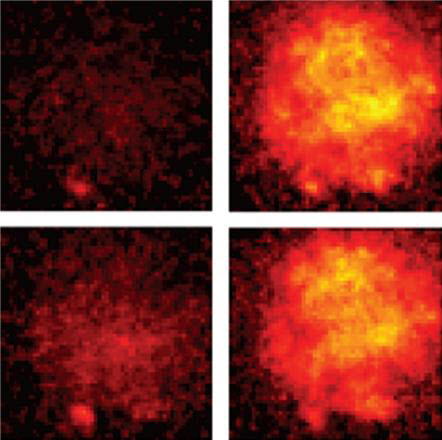
A series of images from a Duke engineering experiment show voltage spreading through a fruitfly neuron over a matter of just 4 milliseconds, a hundred times faster than the blink of an eye. The technology can see impulses as fleeting as 0.2 millisecond — 2000 times faster than a blink. (credit: Yiyang Gong, Duke University)

Researchers at Stanford University and Duke University have developed a new technique for watching the brain’s neurons in action with a temporal (time) resolution of about 0.2 milliseconds — a speed that is just fast enough to capture the action potentials in mammalian brains in real time for the first time.

The researchers combined genetically encoded voltage indicators, which can sense individual action potentials from many cell types in live animals, with a protein that can quickly sense neural voltage potentials with another protein that can amplify its signal output — the brightest fluorescing protein available.

The paper appeared online in Science on November 19, 2015.


Abstract of High-speed recording of neural spikes in awake mice and flies with a fluorescent voltage sensor

Genetically encoded voltage indicators (GEVIs) are a promising technology for fluorescence readout of millisecond-scale neuronal dynamics. Prior GEVIs had insufficient signaling speed and dynamic range to resolve action potentials in live animals. We coupled fast voltage-sensing domains from a rhodopsin protein to bright fluorophores via resonance energy transfer. The resulting GEVIs are sufficiently bright and fast to report neuronal action potentials and membrane voltage dynamics in awake mice and flies, resolving fast spike trains with 0.2-millisecond timing precision at spike detection error rates orders of magnitude better than prior GEVIs. In vivo imaging revealed sensory-evoked responses, including somatic spiking, dendritic dynamics, and intracellular voltage propagation. These results empower in vivo optical studies of neuronal electrophysiology and coding and motivate further advancements in high-speed microscopy.

Quantum entanglement achieved at room temperature in macroscopic semiconductor wafers

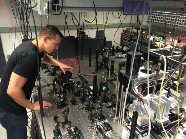
Paul Klimov, a graduate student in the University of Chicago’s Institute for Molecular Engineering, adjusts the intensity of a laser beam during an experiment. (credit: Awschalom Group/University of Chicago)

Researchers in Prof. David Awschalom’s group at the Institute for Molecular Engineering have demonstrated macroscopic entanglement at room temperature and in a small (33 millitesla) magnetic field.

Previously, scientists have overcome the thermodynamic barrier and achieved macroscopic entanglement in solids and liquids by going to ultra-low temperatures (-270 degrees Celsius) and applying huge magnetic fields (1,000 times larger than that of a typical refrigerator magnet) or using chemical reactions.

In an open-access paper published in the Nov. 20 issue of Science Advances, the researchers explain that they used infrared laser light to order (preferentially align) the magnetic states of thousands of electrons and nuclei and then used electromagnetic pulses to entangle them. This procedure caused pairs of electrons and nuclei in a macroscopic 40 micrometer-cubed volume (the volume of a red blood cell) in a silicon carbide (SiC, also known as carborundum) semiconductor wafer to become entangled.

“The ability to produce robust entangled states in an electronic-grade semiconductor at ambient conditions has important implications on future quantum devices,” Awschalom said. In the short term, the research could enable quantum sensors that use entanglement as a resource for beating the sensitivity limit of traditional (non-quantum) sensors and for biological sensing inside a living organism, using entanglement-enhanced magnetic resonance imaging probes, according to the researchers.

They said that it might even be possible in the long term to go from entangled states on the same SiC chip to entangled states across distant SiC chips via macroscopic quantum states, as opposed to single quantum states (in single atoms). Such long-distance entangled states have been proposed for synchronizing global positioning satellites and for communicating information secured from eavesdroppers.

The institute is a partnership of the University of Chicago and and Argonne National Laboratory.


Abstract of Quantum entanglement at ambient conditions in a macroscopic solid-state spin ensemble

Entanglement is a key resource for quantum computers, quantum-communication networks, and high-precision sensors. Macroscopic spin ensembles have been historically important in the development of quantum algorithms for these prospective technologies and remain strong candidates for implementing them today. This strength derives from their long-lived quantum coherence, strong signal, and ability to couple collectively to external degrees of freedom. Nonetheless, preparing ensembles of genuinely entangled spin states has required high magnetic fields and cryogenic temperatures or photochemical reactions. We demonstrate that entanglement can be realized in solid-state spin ensembles at ambient conditions. We use hybrid registers comprising of electron-nuclear spin pairs that are localized at color-center defects in a commercial SiC wafer. We optically initialize 103 identical registers in a 40-μm3 volume (with Embedded Image fidelity) and deterministically prepare them into the maximally entangled Bell states (with 0.88 ± 0.07 fidelity). To verify entanglement, we develop a register-specific quantum-state tomography protocol. The entanglement of a macroscopic solid-state spin ensemble at ambient conditions represents an important step toward practical quantum technology.
 

Physicists plan a miniaturized particle accelerator prototype in five years

Three “accelerators on a chip” made of silicon. A shoebox-sized particle accelerator would use a series of these to boost the energy of electrons. (SLAC National Accelerator Laboratory)

The Gordon and Betty Moore Foundation has awarded $13.5 million to Stanford University for an international effort to build a working particle accelerator the size of a shoebox, based on an “accelerator on a chip” design, a novel technique using laser light to propel electrons through a series of glass chips, with the potential to revolutionize science, medicine, and other fields by dramatically shrinking the size and cost of particle accelerators.

“Can we do for particle accelerators what the microchip industry did for computers?” said SLAC physicist Joel England, an investigator with the 5-year project. “Making them much smaller and cheaper would democratize accelerators, potentially making them available to millions of  people.”


SLAC National Accelerator Laboratory | $13.5M Moore Grant to Develop Working ‘Accelerator on a Chip’ Prototype

“Based on our proposed revolutionary design, this prototype could set the stage for a new generation of ‘tabletop’ accelerators, with unanticipated discoveries in biology and materials science and potential applications in security scanning, medical therapy and X-ray imaging,” said Robert L. Byer, a Stanford professor of applied physics and co-principal investigator for the project who has been working on the idea for 40 years.

The international effort to make a working prototype of the little accelerator was inspired by experiments led by scientists at the SLAC National Accelerator Laboratory (SLAC) and Stanford and, independently, at Friedrich-Alexander University Erlangen-Nuremberg (FAU) in Germany. Both teams demonstrated the potential for accelerating particles with lasers in papers published on the same day in 2013.

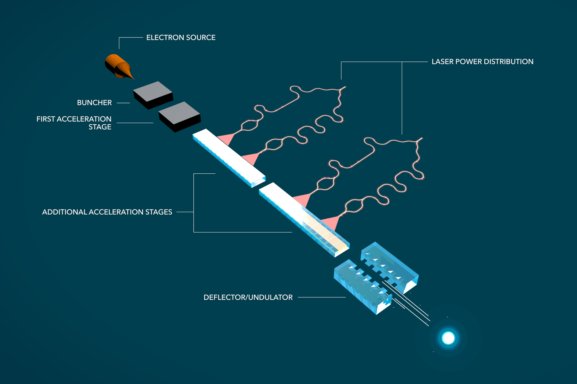
This diagram shows one possible configuration for the shoebox-sized particle accelerator prototype. The Stanford-led team will have to figure out the best way to distribute laser power among the the glass accelerating chips, generate and steer the electrons, shrink the diameter of the electron beam 1,000-fold, and a host of other technical details. (credit: SLAC National Accelerator Laboratory)

In the SLAC/Stanford experiments, published in Nature, electrons were first accelerated to nearly light speed in a SLAC accelerator test facility.  At this point they were going about as fast as they can go, and any additional acceleration would boost their energy, not their speed.

The speeding electrons then entered a chip made of silica glass and traveled through a microscopic tunnel that had tiny ridges carved into its walls. Laser light shining on the chip interacted with those ridges and produced an electrical field that boosted the energy of the passing electrons.

LCLS, the world’s first hard X-ray free-electron laser, pushes science to new extremes with ultrabright, ultrashort pulses that capture atomic-scale snapshots in quadrillionths of a second. These images can reveal never-before-seen structures and properties in matter, and can be compiled to make movies of molecules in motion. (credit: SLAC)

In the experiments, the chip achieved an acceleration gradient, or energy boost over a given distance, roughly 10 times higher than the SLAC linear accelerator can provide. At full potential, this means the 2-mile-long Linac Coherent Light Source could be replaced with a series of accelerator chips 100 meters long — roughly the length of a football field.

In a parallel approach, experiments led by Peter Hommelhoff of FAU and published in Physical Review Letters demonstrated that a laser could also be used to accelerate lower-energy electrons that had not first been boosted to nearly light speed. Both results taken together open the door to a compact particle accelerator.

Challenges

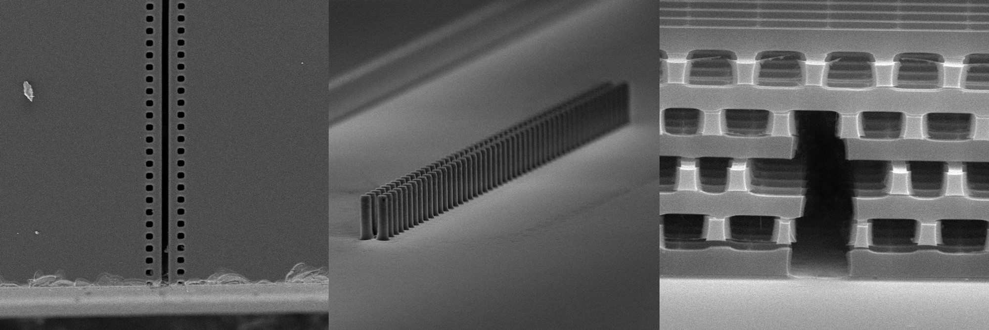
These microscopic images show some of the accelerator-on-a-chip designs being explored by the international collaboration. In each case, laser light shining on the chip boosts the energy of electrons traveling through it. (credit: Left and middle images: Andrew Ceballos, Stanford University, Right image: Chunghun Lee, SLAC)

For the past 75 years, particle accelerators have been an essential tool for physics, chemistry, biology and medicine, leading to multiple Nobel prize-winning discoveries. But without new technology to reduce the cost and size of high-energy accelerators, progress in particle physics and structural biology could stall.

The challenges of building the prototype accelerator are substantial, the scientists said. Demonstrating that a single chip works was an important step; now they must work out the optimal chip design and the best way to generate and steer electrons, distribute laser power among multiple chips and make electron beams that are 1,000 times smaller in diameter to go through the microscopic chip tunnels, among a host of other technical details.

The Stanford-led collaboration includes world-renowned experts in accelerator physics, laser physics, nanophotonics and nanofabrication. SLAC and two other national laboratories — Deutsches Elektronen-Synchrotron (DESY) in Germany and Paul Scherrer Institute in Switzerland — will contribute expertise and make their facilities available for experiments. In addition to FAU, five other universities are involved in the effort:  University of California, Los Angeles, Purdue University, University of Hamburg, the Swiss Federal Institute of Technology in Lausanne (EPFL) and Technical University of Darmstadt.


Abstract of Demonstration of electron acceleration in a laser-driven dielectric microstructure

The enormous size and cost of current state-of-the-art accelerators based on conventional radio-frequency technology has spawned great interest in the development of new acceleration concepts that are more compact and economical. Micro-fabricated dielectric laser accelerators (DLAs) are an attractive approach, because such dielectric microstructures can support accelerating fields one to two orders of magnitude higher than can radio-frequency cavity-based accelerators. DLAs use commercial lasers as a power source, which are smaller and less expensive than the radio-frequency klystrons that power today’s accelerators. In addition, DLAs are fabricated via low-cost, lithographic techniques that can be used for mass production. However, despite several DLA structures having been proposed recently, no successful demonstration of acceleration in these structures has so far been shown. Here we report high-gradient (beyond 250 MeV m−1) acceleration of electrons in a DLA. Relativistic (60-MeV) electrons are energy-modulated over 563 ± 104 optical periods of a fused silica grating structure, powered by a 800-nm-wavelength mode-locked Ti:sapphire laser. The observed results are in agreement with analytical models and electrodynamic simulations. By comparison, conventional modern linear accelerators operate at gradients of 10–30 MeV m−1, and the first linear radio-frequency cavity accelerator was ten radio-frequency periods (one metre) long with a gradient of approximately 1.6 MeV m−1. Our results set the stage for the development of future multi-staged DLA devices composed of integrated on-chip systems. This would enable compact table-top accelerators on the MeV–GeV (106–109 eV) scale for security scanners and medical therapy, university-scale X-ray light sources for biological and materials research, and portable medical imaging devices, and would substantially reduce the size and cost of a future collider on the multi-TeV (1012 eV) scale.