‘Designless’ nanoscale logic circuits resemble Darwinian evolution and neural networks

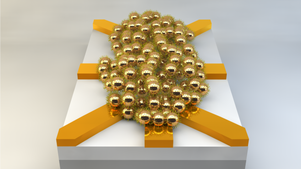
Illustration of a nanoparticle network (about 200 nanometers in diameter). By applying electrical signals at the electrodes (yellow), and using artificial evolution, this disordered network can be configured into useful logic circuits. (credit: University of Twente)

Researchers at the University of Twente in The Netherlands have designed and demonstrated working electronic logic circuits produced using methods that resemble Darwinian evolution and neural networks like the human brain.

In a radical “designless” approach, the researchers used a 200-nanometer-wide cluster of 20-nanometer gold nanoparticles. They applied a series of voltages to eight electrodes and determined the resulting set of 16 different two-input Boolean logic gates.

Artificial evolution

Instead of designing logic circuits with specified functions, as with conventional transistors, this approach works around — or can even take advantage of — any material defects.

To do this, the researchers used an artificial evolution model — one that runs in less than an hour, rather than millions of years. “Natural evolution has led to powerful ‘computers’ like the human brain, which can solve complex problems in an energy-efficient way,” the researchers note. “Nature exploits complex networks that can execute many tasks in parallel.”

“This is the first time that scientists have succeeded in realizing robust electronics with small dimensions that can compete with commercial technology.”
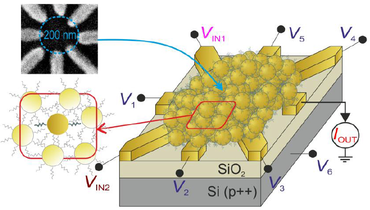
Schematic device layout of the disordered network of gold nanoparticles, separated by ~1 nm 1-octanethiols, in between eight titanium-gold electrodes, as shown in the scanning electron micrograph (top inset). The gold nanoparticles act as single-electron transistors (SETs) at low temperature (<15 K). (credit: S. K. Bose, et al./Nature Nanotechnology)

Conventional transistors are limited to a handful of atoms. It would a major challenge to produce chips in which the millions of transistors required have the same characteristics, according to the researchers from the Twente MESA+ Institute for Nanotechnology and the CTIT Institute for ICT Research. Current transistor designs are also limited by their energy consumption, which is reaching unacceptable levels.

According to University of Twente prof. Wilfred van der Wiel, the logic circuits they discovered currently have limited computing power. “But with this research we have delivered a proof of principle. By scaling up the system, real added value will be produced in the future. This type of circuitry uses much less energy, both in production and use.” The researchers anticipate a wide range of applications — for example, in portable electronics and in the medical world.

“By choosing a smaller nanoparticle diameter, and scaling down the electrode geometry accordingly, our network would not only further reduce area, but room-temperature operation would come into sight as well,” the researchers note in a paper in the journal Nature Nanotechnology.

Mimicking brain-like systems

The researchers also contrast their “designless” reconfigurable approach with massively parallel (but still design-constrained) architectures such as IBM’s TrueNorth brain-inspired chip.

“An especially interesting avenue to explore is the suitability of this system for advanced functionality that is hard (or expensive) to realize in a conventional architecture, such as pattern recognition by mimicking brain-like systems, or simulations of complex physical systems,” the researchers note in the paper. “Our evolutionary approach works around device-to-device variations at the nanoscale and the accompanying uncertainties in performance, which is becoming more and more a bottleneck for the miniaturization of conventional electronic circuits.”


Abstract of Evolution of a designless nanoparticle network into reconfigurable Boolean logic

Natural computers exploit the emergent properties and massive parallelism of interconnected networks of locally active components. Evolution has resulted in systems that compute quickly and that use energy efficiently, utilizing whatever physical properties are exploitable. Man-made computers, on the other hand, are based on circuits of functional units that follow given design rules. Hence, potentially exploitable physical processes, such as capacitive crosstalk, to solve a problem are left out. Until now, designless nanoscale networks of inanimate matter that exhibit robust computational functionality had not been realized. Here we artificially evolve the electrical properties of a disordered nanomaterials system (by optimizing the values of control voltages using a genetic algorithm) to perform computational tasks reconfigurably. We exploit the rich behaviour that emerges from interconnected metal nanoparticles, which act as strongly nonlinear single-electron transistors, and find that this nanoscale architecture can be configured in situ into any Boolean logic gate. This universal, reconfigurable gate would require about ten transistors in a conventional circuit. Our system meets the criteria for the physical realization of (cellular) neural networks: universality (arbitrary Boolean functions), compactness, robustness and evolvability, which implies scalability to perform more advanced tasks. Our evolutionary approach works around device-to-device variations and the accompanying uncertainties in performance. Moreover, it bears a great potential for more energy-efficient computation, and for solving problems that are very hard to tackle in conventional architectures.

Living implants

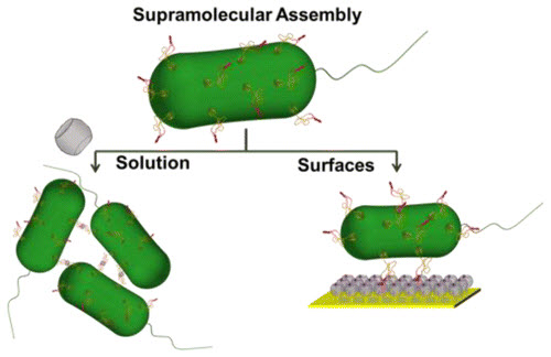
“Living implant” using a bacterial strain (credit: Shrikrishnan Sankaran et al./ACS Nano)

A method for merging bacteria in human cells as “living implants” has been developed by University of Twente researchers. The implants could include stents equipped with bacteria on which endothelial cells (cells that form the lining of blood vessels) can grow, or bacteria that can release medicines in specific parts of the body.

They achieved this by supramolecular assembly, modifying the DNA of E. coli bacteria in such a way that a small molecule called Cucurbit[8]uril attaches to a protein on the cell membrane. This substance could then attach to other building blocks, forming a sort of natural Velcro.

The research was published in the journal ACS Nano. It was sponsored by the European Union.


Abstract of Incorporating Bacteria as a Living Component in Supramolecular Self-Assembled Monolayers through Dynamic Nanoscale Interactions

Supramolecular assemblies, formed through noncovalent interactions, has become particularly attractive to develop dynamic and responsive architectures to address living systems at the nanoscale. Cucurbit[8]uril (CB[8]), a pumpkin shaped macrocylic host molecule, has been successfully used to construct various self-assembled architectures for biomedical applications since it can simultaneously bind two aromatic guest molecules within its cavity. Such architectures can also be designed to respond to external stimuli. Integrating living organisms as an active component into such supramolecular architectures would add a new dimension to the capabilities of such systems. To achieve this, we have incorporated supramolecular functionality at the bacterial surface by genetically modifying a transmembrane protein to display a CB[8]-binding motif as part of a cystine-stabilized miniprotein. We were able to confirm that this supramolecular motif on the bacterial surface specifically binds CB[8] and forms multiple intercellular ternary complexes leading to aggregation of the bacterial solution. We performed various aggregation experiments to understand how CB[8] interacts with this bacterial strain and also demonstrate that it can be chemically reversed using a competitor. To confirm that this strain can be incorporated with a CB[8] based architecture, we show that the bacterial cells were able to adhere to CB[8] self-assembled monolayers (SAMs) on gold and still retain considerable motility for several hours, indicating that the system can potentially be used to develop supramolecular bacterial biomotors. The bacterial strain also has the potential to be combined with other CB[8] based architectures like nanoparticles, vesicles and hydrogels.

First optical ‘rectenna’ converts light to DC current

This schematic shows the components of the optical rectenna developed at the Georgia Institute of Technology (credit: Thomas Bougher, Georgia Tech)

Using nanometer-scale components, Georgia Institute of Technology researchers have demonstrated the first optical rectenna, a device that combines the functions of an antenna and a rectifier diode to convert light directly into DC current.

Based on multiwall carbon nanotubes and tiny rectifiers fabricated onto them, the optical rectennas could provide a new technology for energy harvesters, including photodetectors that would operate without the need for cooling, convert waste heat to electricity,  and ultimately, efficiently capture solar energy.

In the new devices, the carbon nanotubes act as antennas to capture light from the Sun or other sources. As the waves of light hit the nanotube antennas, they create an oscillating charge that moves through rectifier devices attached to them. The rectifiers switch on and off at record high petahertz speeds, creating a small direct current.

The efficiency of the devices demonstrated so far remains below one percent, but the researchers hope to boost that output by using billions of rectennas in an array, which could produce significant current. They believe a rectenna with commercial potential may be available within a year.

“We could ultimately make solar cells that are twice as efficient at a cost that is ten times lower, and that is to me an opportunity to change the world in a very big way” said Baratunde Cola, an associate professor in the George W. Woodruff School of Mechanical Engineering at Georgia Tech. “As a robust, high-temperature detector, these rectennas could be a completely disruptive technology if we can get to one percent efficiency. If we can get to higher efficiencies, we could apply it to energy conversion technologies and solar energy capture.”

A carbon nanotube optical rectenna converts green laser light to electricity in the laboratory of Baratunde Cola at the Georgia Institute of Technology (credit: Rob Felt, Georgia Tech)

“A rectenna is basically an antenna coupled to a diode, but when you move into the optical spectrum, that usually means a nanoscale antenna coupled to a metal-insulator-metal diode,” Cola explained. “The closer you can get the antenna to the diode, the more efficient it is. So the ideal structure uses the antenna as one of the metals in the diode – which is the structure we made.”

The rectennas fabricated by Cola’s group are grown on rigid substrates, but the goal is to grow them on a foil or other material that would produce flexible solar cells or photodetectors.

Cola sees the rectennas built so far as simple proof of principle. “We think we can reduce the resistance by several orders of magnitude just by improving the fabrication of our device structures,” he said. “Based on what others have done and what the theory is showing us, I believe that these devices could get to greater than 40 percent efficiency.”

The research, supported by the Defense Advanced Research Projects Agency (DARPA), the Space and Naval Warfare (SPAWAR) Systems Center and the Army Research Office (ARO), is reported September 28 in the journal Nature Nanotechnology.

* Developed in the 1960s and 1970s, rectennas have operated at wavelengths as short as ten micrometers, but for more than 40 years researchers have been attempting to make devices at optical wavelengths. There were many challenges: making the antennas small enough to couple optical wavelengths, and fabricating a matching rectifier diode small enough and able to operate fast enough to capture the electromagnetic wave oscillations. But the potential of high efficiency and low cost kept scientists working on the technology.

Fabricating the rectennas begins with growing forests of vertically-aligned carbon nanotubes on a conductive substrate. Using atomic layer chemical vapor deposition, the nanotubes are coated with an aluminum oxide material to insulate them. Finally, physical vapor deposition is used to deposit optically-transparent thin layers of calcium then aluminum metals atop the nanotube forest. The difference of work functions between the nanotubes and the calcium provides a potential of about two electron volts, enough to drive electrons out of the carbon nanotube antennas when they are excited by light.

In operation, oscillating waves of light pass through the transparent calcium-aluminum electrode and interact with the nanotubes. The metal-insulator-metal junctions at the nanotube tips serve as rectifiers switching on and off at femtosecond intervals, allowing electrons generated by the antenna to flow one way into the top electrode. Ultra-low capacitance, on the order of a few attofarads, enables the 10-nanometer diameter diode to operate at these exceptional frequencies.


Georgia Tech | Using nanometer-scale components, researchers have demonstrated the first optical rectenna, a device that combines the functions of an antenna and a rectifier diode to convert light directly into DC current.


Abstract of A carbon nanotube optical rectenna

An optical rectenna—a device that directly converts free-propagating electromagnetic waves at optical frequencies to direct current—was first proposed over 40 years ago, yet this concept has not been demonstrated experimentally due to fabrication challenges at the nanoscale. Realizing an optical rectenna requires that an antenna be coupled to a diode that operates on the order of 1 pHz (switching speed on the order of 1 fs). Diodes operating at these frequencies are feasible if their capacitance is on the order of a few attofarads, but they remain extremely difficult to fabricate and to reliably couple to a nanoscale antenna. Here we demonstrate an optical rectenna by engineering metal–insulator–metal tunnel diodes, with a junction capacitance of ∼2 aF, at the tip of vertically aligned multiwalled carbon nanotubes (∼10 nm in diameter), which act as the antenna. Upon irradiation with visible and infrared light, we measure a d.c. open-circuit voltage and a short-circuit current that appear to be due to a rectification process (we account for a very small but quantifiable contribution from thermal effects). In contrast to recent reports of photodetection based on hot electron decay in a plasmonic nanoscale antenna, a coherent optical antenna field appears to be rectified directly in our devices, consistent with rectenna theory. Finally, power rectification is observed under simulated solar illumination, and there is no detectable change in diode performance after numerous current–voltage scans between 5 and 77 °C, indicating a potential for robust operation.

Ultrafast lasers enable 3-D micropatterning of biocompatible hydrogels

Illustration of laser-based micropatterning of silk hydrogels. The transparent gels enable the laser’s photons (pink) to be absorbed more than 10 times deeper than with other materials without damaging the cells (green) surrounding the letters (credit: M.B. A)

Tufts University biomedical engineers have developed low-energy, ultrafast laser technology for micropatterning high-resolution, 3-D structures in silk-protein hydrogels.

Micropatterning is used to bring oxygen and nutrients to rapidly proliferating cells in an engineered tissue scaffold. The goal is “to controllably guide cell growth and create an artificial vasculature (blood vessel system) within an already densely seeded silk hydrogel,” said Fiorenzo G. Omenetto, Ph.D., senior author of a paper on the work in PNAS Early Edition published September 15 online before print.

Current patterning techniques allow for the production of random, micrometer-scale pores and also the creation of larger channels that are hundreds of micrometers in diameter, but there is little in between.

The Tufts researchers used the ultrafast femtosecond laser to generate scalable, high-resolution 3-D pores (voids) within silk protein hydrogel, a soft, transparent biomaterial that supports cell growth and allows cells to penetrate deep within it. The researchers were able to create pores at multiple scales as small as 10 micrometers and as large at 400 micrometers over a large volume.

The transparent silk gels also enabled the laser’s photons to be absorbed nearly 1 cm below the surface of the gel — more than ten times deeper than with other materials — without damaging adjacent material.

The laser treatment can be done while keeping the cell culture sealed and sterile. Unlike most 3-D printing, this technique does not require photoinitiators (compounds that promote photoreactivity but are typically not biocompatible).

Omenetto is associate dean for research, professor of biomedical engineering and Frank C. Doble professor at Tufts School of Engineering and also holds an appointment in physics in the School of Arts and Sciences.

The research team reported similar results in vitro and in a preliminary in vivo study in mice.


Abstract of Laser-based three-dimensional multiscale micropatterning of biocompatible hydrogels for customized tissue engineering scaffolds

Light-induced material phase transitions enable the formation of shapes and patterns from the nano- to the macroscale. From lithographic techniques that enable high-density silicon circuit integration, to laser cutting and welding, light–matter interactions are pervasive in everyday materials fabrication and transformation. These noncontact patterning techniques are ideally suited to reshape soft materials of biological relevance. We present here the use of relatively low-energy (< 2 nJ) ultrafast laser pulses to generate 2D and 3D multiscale patterns in soft silk protein hydrogels without exogenous or chemical cross-linkers. We find that high-resolution features can be generated within bulk hydrogels through nearly 1 cm of material, which is 1.5 orders of magnitude deeper than other biocompatible materials. Examples illustrating the materials, results, and the performance of the machined geometries in vitro and in vivo are presented to demonstrate the versatility of the approach.

How to make 3-D objects totally disappear

This image shows a 3-D illustration of a metasurface skin cloak made from an ultrathin layer of nanoantennas (gold blocks) covering an arbitrarily shaped object. When activated, light reflects off the cloak (red arrows) as if it were reflecting off a flat mirror. (credit: Image courtesy of Xiang Zhang group, Berkeley Lab/UC Berkeley)

An ultra-thin invisibility “skin” cloak that can conform to the shape of an object and conceal it from detection with visible light has been developed by scientists at Lawrence Berkeley National Laboratory (Berkeley Lab) and the University of California (UC) Berkeley.

Working with blocks of gold nanoantennas, the Berkeley researchers created a “skin cloak” just 80 nanometers in thickness that was wrapped around a three-dimensional object about the size of a few biological cells and shaped with multiple bumps and dents. The surface of the skin cloak was meta-engineered to reflect light waves, making the object invisible to optical detection when the cloak is activated.

“This is the first time a 3D object of arbitrary shape has been cloaked from visible light,” said Xiang Zhang, director of Berkeley Lab’s Materials Sciences Division. “Our ultra-thin cloak now looks like a coat. It is easy to design and implement, and is potentially scalable for hiding macroscopic objects.”

Zhang, who holds the Ernest S. Kuh Endowed Chair at UC Berkeley and is a member of the Kavli Energy NanoSciences Institute at Berkeley (Kavli ENSI), is the corresponding author of a paper describing this research in the journal Science.

Click to see an animation of an invisibility cloak that makes a 3-D object disappear (credit: Zhang group)

It is the scattering of light from its interaction with matter that enables us to detect and observe objects. The rules that govern these interactions in natural materials can be circumvented in metamaterials, whose optical properties arise from their physical structure rather than their chemical composition.

For the past ten years, Zhang and his research group have been pushing the boundaries of how light interacts with metamaterials, managing to curve the path of light or bend it backwards, phenomena not seen in natural materials, and to render objects optically undetectable. In the past, their metamaterial-based optical carpet cloaks were bulky and hard to scale up, and entailed a phase difference between the cloaked region and the surrounding background that made the cloak itself detectable, though what it concealed was not.

Now you see it, now you don’t

In the new study, the researchers used red light to illuminate an arbitrarily shaped 3-D sample object about 1,300 square micrometers in area and wrapped in the gold nanoantenna skin cloak. The light reflected off the surface of the skin cloak was identical to light reflected off a flat mirror, making the object underneath it invisible even by phase-sensitive detection. The cloak can be turned “on” or “off” simply by switching the polarization of the nanoantennas.

“A phase shift provided by each individual nanoantenna fully restores both the wavefront and the phase of the scattered light so that the object remains perfectly hidden,” says co-lead author Zi Jing Wong, also a member of Zhang’s research group.

According the researchers. the ability to manipulate the interactions between light and metamaterials offers future prospects for technologies such as high-resolution optical microscopes and superfast optical computers, and for hiding the detailed layout of microelectronic components or for security encryption purposes.

At the macroscale, among other applications, invisibility cloaks could prove useful for 3D displays, they add.


Abstract of An ultrathin invisibility skin cloak for visible light

Metamaterial-based optical cloaks have thus far used volumetric distribution of the material properties to gradually bend light and thereby obscure the cloaked region. Hence, they are bulky and hard to scale up and, more critically, typical carpet cloaks introduce unnecessary phase shifts in the reflected light, making the cloaks detectable. Here, we demonstrate experimentally an ultrathin invisibility skin cloak wrapped over an object. This skin cloak conceals a three-dimensional arbitrarily shaped object by complete restoration of the phase of the reflected light at 730-nanometer wavelength. The skin cloak comprises a metasurface with distributed phase shifts rerouting light and rendering the object invisible. In contrast to bulky cloaks with volumetric index variation, our device is only 80 nanometer (about one-ninth of the wavelength) thick and potentially scalable for hiding macroscopic objects.

Liquid water flows on today’s Mars, NASA confirms

NASA says these dark, narrow, 100 meter-long streaks called recurring slope lineae flowing downhill on Mars appear to have been formed by contemporary flowing water (credit: NASA/JPL/University of Arizona)

New findings from NASA’s Mars Reconnaissance Orbiter (MRO) provide the strongest evidence yet that liquid water flows intermittently on present-day Mars, NASA announced today.

Researchers detected darkish signatures of hydrated minerals on slopes in several locations that appear to ebb and flow over time, based on spectrometer data. The signatures darken and appear to flow down steep slopes during warm seasons, and then fade in cooler seasons.

“This is a significant development, as it appears to confirm that water — albeit briny — is flowing today on the surface of Mars,” said John Grunsfeld, astronaut and associate administrator of NASA’s Science Mission Directorate in Washington.

“We found the hydrated salts only when the seasonal features were widest, which suggests that either the dark streaks themselves or a process that forms them is the source of the hydration. In either case, the detection of hydrated salts on these slopes means that water plays a vital role in the formation of these streaks,” said Lujendra Ojha of the Georgia Institute of Technology in Atlanta, lead author of a report on these findings published Sept. 28 by Nature Geoscience.

Ojha and his co-authors interpret the spectral signatures as caused by hydrated minerals called perchlorates. On Earth, naturally produced perchlorates are concentrated in deserts, and some types of perchlorates can be used as rocket propellant.

Other co-authors are affiliated with NASA Ames Research Center, Johns Hopkins University Applied Physics Laboratory, University of Arizona Lunar and Planetary Laboratory, Southwest Research Institute, and Laboratoire de Planétologie et Géodynamique.


JPL | Animation of Site of Seasonal Flows in Hale Crater, Mars

These self-propelled microscopic carbon-capturing motors may reduce carbon-dioxide levels in oceans

Nanoengineers have invented tiny tube-shaped micromotors that zoom around in water and efficiently remove carbon dioxide. The surfaces of the micromotors are functionalized with the enzyme carbonic anhydrase, which enables the motors to help rapidly convert carbon dioxide to calcium carbonate. (credit: Laboratory for Nanobioelectronics, UC San Diego Jacobs School of Engineering)

Nanoengineers at the University of California, San Diego have designed enzyme-functionalized micromotors the size of red blood cells that rapidly zoom around in water, remove carbon dioxide, and convert it into a usable solid form.

The proof-of-concept study represents a promising route to mitigate the buildup of carbon dioxide, a major greenhouse gas in the environment, said the researchers.

The team, led by distinguished nanoengineering professor and chair Joseph Wang, published the work this month in the journal Angewandte Chemie.

In their experiments, the nanoengineers demonstrated that the micromotors rapidly decarbonated water solutions that were saturated with carbon dioxide. Within five minutes, the micromotors removed 90 percent of the carbon dioxide from a solution of deionized water.

The micromotors were just as effective in a sea-water solution and removed 88 percent of the carbon dioxide in the same time frame.

“In the future, we could potentially use these micromotors as part of a water treatment system, like a water decarbonation plant,” said Kevin Kaufmann, an undergraduate researcher in Wang’s lab and a co-author of the study.

The micromotors are essentially six-micrometer-long tubes that help rapidly convert carbon dioxide into calcium carbonate, a solid mineral found in eggshells, the shells of various marine organisms, calcium supplements and cement. The micromotors have an outer polymer surface that holds the enzyme carbonic anhydrase, which speeds up the reaction between carbon dioxide and water to form bicarbonate. Calcium chloride, which is added to the water solutions, helps convert bicarbonate to calcium carbonate.

The fast, continuous motion of the micromotors in solution makes the micromotors extremely efficient at removing carbon dioxide from water, according to the researchers. The team explained that the micromotors’ autonomous movement induces efficient solution mixing, leading to faster carbon dioxide conversion.

Self-propulsion from oxygen gas bubbles

To fuel the micromotors in water, researchers added hydrogen peroxide, which reacts with the inner platinum surface of the micromotors to generate a stream of oxygen gas bubbles that propel the micromotors around. When released in water solutions containing as little as two to four percent hydrogen peroxide, the micromotors reached speeds of more than 100 micrometers per second.

Vdeo frames showing the movement of a micromotor in sea water (credit: Laboratory for Nanobioelectronics, UC San Diego Jacobs School of Engineering)

However, the use of hydrogen peroxide as the micromotor fuel is a drawback because it is an extra additive and requires the use of expensive platinum materials to build the micromotors. As a next step, researchers are planning to make carbon-capturing micromotors that can be propelled by water.

“If the micromotors can use the environment as fuel, they will be more scalable, environmentally friendly and less expensive,” said Kaufmann.


Abstract of Micromotor-Based Biomimetic Carbon Dioxide Sequestration: Towards Mobile Microscrubbers

We describe a mobile CO2 scrubbing platform that offers a greatly accelerated biomimetic sequestration based on a self-propelled carbonic anhydrase (CA) functionalized micromotor. The CO2 hydration capability of CA is coupled with the rapid movement of catalytic micromotors, and along with the corresponding fluid dynamics, results in a highly efficient mobile CO2 scrubbing microsystem. The continuous movement of CA and enhanced mass transport of the CO2 substrate lead to significant improvements in the sequestration efficiency and speed over stationary immobilized or free CA platforms. This system is a promising approach to rapid and enhanced CO2 sequestration platforms for addressing growing concerns over the buildup of greenhouse gas.

DNA-based nanodevices for molecular medicine: an overview

Virus-protein-coated DNA origami nanostructures. With the help of protein encapsulation, DNA origamis can be transported into human cells much more efficiently. (credit: Veikko Linko and Mauri Kostiainen)

KurzweilAI has covered a wide variety of research projects that explore how DNA molecules can be assembled into complex nanostructures for molecular-scale diagnostics, smart drug-delivery, and other uses. For example, tailored DNA structures could find targeted cancer cells and release their molecular payload (drugs or antibodies) selectively.

An article written by researchers from Aalto University just published in Trends in Biotechnology journal, comparing biological DNA-nanomachine developments and their uses, should help put this varied research in perspective.

The authors explain that “the field of structural DNA nanotechnology started around 30 years ago when Ned Seeman performed pioneering research with DNA junctions and lattice. … The key player in the fast development of DNA nanotechnology was the invention of DNA origami in 2006. The DNA origami method is based on folding a long
single-stranded ‘DNA scaffold strand’ into a customized shape with a set of short synthetic strands that act as ‘staples’ to bind the overall structure together.”

“This method is the starting point for practically all other straightforward design approaches available today,” says Veikko Linko, an Academy of Finland postdoctoral researcher from Biohybrid Materials Group and first author.

The accurate shape of a DNA origami nanostructure can be used to create entirely metallic nanoparticles on silicon substrates. (credit: Veikko Linko, Boxuan Shen and Mauri Kostiainen with permission from Royal Society of Chemistry)

Versatile DNA nanostructures

The most important feature of a DNA-based nanostructure is its modularity, the authors note. DNA structures can be fabricated with nanometer-precision, and other molecules such as RNA, proteins, peptides and drugs can be anchored to them with the same resolution.

Such a high precision can be exploited in creating nanosized optical devices as well as molecular platforms and bar codes for various imaging techniques and analytics.

The author further point out that for molecular medicine, DNA-based devices could be used for detecting single molecules and modulating cell signaling. In the near future, highly sophisticated DNA robots could even be used in creating artificial immune systems, they note.

In addition, a system based on tailored DNA devices could help to avoid unnecessary drug treatments, since programmed DNA-nanorobots could detect various agents from the blood stream, and immediately start the battle against disease.


Abstract of DNA Nanostructures as Smart Drug-Delivery Vehicles and Molecular Devices

DNA molecules can be assembled into custom predesigned shapes via hybridization of sequence-complementary domains. The folded structures have high spatial addressability and a tremendous potential to serve as platforms and active components in a plethora of bionanotechnological applications. DNA is a truly programmable material, and its nanoscale engineering thus opens up numerous attractive possibilities to develop novel methods for therapeutics. The tailored molecular devices could be used in targeting cells and triggering the cellular actions in the biological environment. In this review we focus on the DNA-based assemblies – primarily DNA origami nanostructures – that could perform complex tasks in cells and serve as smart drug-delivery vehicles in, for example, cancer therapy, prodrug medication, and enzyme replacement therapy.

Brain-computer interface enables paralyzed man to walk without robotic support

A BCI system allows a man whose legs had been paralyzed to walk without robotic support (credit: courtesy of UCI’s Brain Computer Interface Lab)

A novel brain-computer-interface (BCI) technology created by University of California, Irvine researchers has allowed a paraplegic man to walk for a short distance, unaided by an exoskeleton or other types of robotic support.

The male participant, whose legs had been paralyzed for five years, walked along a 12-foot course using an electroencephalogram (EEG) brain-computer-interface system that lets the brain bypass the spinal cord to send messages to the legs.

It takes electrical signals from the subject’s brain, processes them through a computer algorithm, and fires them off to electrodes placed around the knees that trigger movement in the leg muscles.

“Even after years of paralysis, the brain can still generate robust brain waves that can be harnessed to enable basic walking,” said UCI biomedical engineer Zoran Nenadic, an associate professor of biomedical engineering.

“We showed that you can restore intuitive, brain-controlled walking after a complete spinal cord injury. This noninvasive system for leg muscle stimulation is a promising method and is an advance of our current brain-controlled systems that use virtual reality or a robotic exoskeleton.”

Study results of this preliminary proof-of-concept study appear in an open-access paper in the Journal of NeuroEngineering & Rehabilitation. The research was supported by a National Science Foundation grant.

Training and therapy process

Months of mental training to reactivate the brain’s walking ability and physical therapy were needed for the study participant to reach the stage where he could take steps. Wearing an EEG cap to read his brain waves, he was first asked to think about moving his legs. The brain waves this created were processed through a computer algorithm designed to isolate brain signals specifically related to leg movement.

The subject was first trained to control an avatar in a virtual reality environment, which validated the specific brain wave signals produced by the algorithm. This training process yielded a custom-made system, Nenadic said, so that when the participant sought to initiate leg movement, the computer algorithm could process the brain waves into signals that could stimulate his leg muscles.


UCI | Person with Paraplegia Uses a Brain-Computer Interface to Regain Overground Walking

To make this work, the subject required extensive physical therapy to recondition and strengthen his leg muscles. Then, with the EEG cap on, he practiced walking while suspended 5 centimeters above the floor, so he could freely move his legs without having to support himself. Finally, he translated these skills to the ground, wearing a body-weight support system and pausing to prevent falls.

Since this study involved a single patient, further research is needed to establish whether the results can be duplicated in a larger population of individuals with paraplegia, said An Do, a neurologist and an assistant clinical professor of neurology.

“Once we’ve confirmed the usability of this noninvasive system, we can look into invasive means, such as brain implants,” she said. “We hope that an implant could achieve an even greater level of prosthesis control because brain waves are recorded with higher quality. In addition, such an implant could deliver sensation back to the brain, enabling the user to feel his legs.”


Abstract of The feasibility of a brain-computer interface functional electrical stimulation system for the restoration of overground walking after paraplegia

Background: Direct brain control of overground walking in those with paraplegia due to spinal cord injury (SCI) has not been achieved. Invasive brain-computer interfaces (BCIs) may provide a permanent solution to this problem by directly linking the brain to lower extremity prostheses. To justify the pursuit of such invasive systems, the feasibility of BCI controlled overground walking should first be established in a noninvasive manner. To accomplish this goal, we developed an electroencephalogram (EEG)-based BCI to control a functional electrical stimulation (FES) system for overground walking and assessed its performance in an individual with paraplegia due to SCI.

Methods: An individual with SCI (T6 AIS B) was recruited for the study and was trained to operate an EEG-based BCI system using an attempted walking/idling control strategy. He also underwent muscle reconditioning to facilitate standing and overground walking with a commercial FES system. Subsequently, the BCI and FES systems were integrated and the participant engaged in several real-time walking tests using the BCI-FES system. This was done in both a suspended, off-the-ground condition, and an overground walking condition. BCI states, gyroscope, laser distance meter, and video recording data were used to assess the BCI performance.

Results: During the course of 19 weeks, the participant performed 30 real-time, BCI-FES controlled overground walking tests, and demonstrated the ability to purposefully operate the BCI-FES system by following verbal cues. Based on the comparison between the ground truth and decoded BCI states, he achieved information transfer rates >3 bit/s and correlations >0.9. No adverse events directly related to the study were observed.

Conclusion: This proof-of-concept study demonstrates for the first time that restoring brain-controlled overground walking after paraplegia due to SCI is feasible. Further studies are warranted to establish the generalizability of these results in a population of individuals with paraplegia due to SCI. If this noninvasive system is successfully tested in population studies, the pursuit of permanent, invasive BCI walking prostheses may be justified. In addition, a simplified version of the current system may be explored as a noninvasive neurorehabilitative therapy in those with incomplete motor SCI.

Pushing the resolution and exposure-time limits of lensless imaging

With “coherent diffraction imaging,” extreme ultraviolet light scatters off a sample and produces a diffraction pattern, which a computer then analyzes to reconstruct an image of the target material (credit: Dr. Michael Zürch, Friedrich Schiller University Jena, Germany)

Physicists at Friedrich Schiller University in Germany are pushing the boundaries of nanoscale imaging by shooting ultra-high-resolution, real-time images in extreme ultraviolet light — without lenses. The new method could be used to study everything from semiconductor chips to cancer cells, the scientists say.

They are improving a lensless imaging technique called “coherent diffraction imaging,” which has been around since the 1980s. To take a picture with this method, scientists fire an extreme ultraviolet laser or X-ray at a target. The light scatters off, and some of those photons interfere with one another and find their way onto a detector, creating a diffraction pattern.

Diffraction pattern of red laser beam (credit: Wisky/Wikipedia)

By analyzing that pattern, a computer then reconstructs the path those photons must have taken, which generates an image of the target material.

But the quality of the images depends on the radiation source. Traditionally, researchers have used big, powerful X-ray beams like the one at the SLAC National Accelerator Laboratory, which can pump out lots of photons.

To make the process more accessible, researchers have developed smaller machines using coherent laser-like beams, which are cheaper but produce lower-quality images and require short focal lengths (similar to placing a specimen close to a microscope to boost the magnification) and long exposure times.

As in conventional photography, that rules out large, real-time images.

Now, Michael Zürch and his research team have built an ultrafast laser that fires extreme UV photons 100 times faster than previous table-top machines and is able to snap an image at a resolution of 26 nanometers (the size of a blackline walnut virus) — almost the theoretical diffraction limit for the 33-nanometers UV light used. They were also able to get real-time images at a rate of one per second at the reduced resolution of 80 nanometers.

The prospect of high-resolution, real-time imaging using a relatively low-cost, small setup could lead to all kinds of applications, Zürch said. Engineers could use this to hunt for tiny defects in semiconductor chips. Biologists could zoom in on the organelles that make up a cell. Eventually, he said, the researchers might be able to reach shorter exposure times and higher resolution levels.

The team will present their work at Frontiers in Optics, the Optical Society’s annual meeting and conference in San Jose, California on October 22, 2015.