Lightweight solar cells track the sun, providing 40 percent more energy than fixed cells

By borrowing from kirigami, the ancient Japanese art of paper cutting, researchers at the University of Michigan have developed solar cells that can track the sun. A flat plastic sheet backing the solar cells splits into wavy, connected ribbons when stretched. The tilt of each of the cells depends on the stretching, a simple mechanism for tracking the sun across the sky. (credit: Aaron Lamoureux)

University of Michigan engineers have developed an innovative array of solar cells that can capture up to 40 percent more energy than conventional fixed solar cells. The trick: borrowing from kirigami (the ancient Japanese art of paper cutting), the solar cells are aimed at different angles, allowing for part of the array to be always perpendicular to the Sun’s rays.

“The design takes what a large tracking solar panel does and condenses it into something that is essentially flat,” said Aaron Lamoureux, a doctoral student in materials science and engineering and first author on the open-access paper in Nature Communications. Residential rooftops would need significant reinforcing to support the weight of conventional costly sun-tracking systems, he said.

Tilting toward the Sun

Cuts in plastic substrate allow for an array of solar cells titled at different angles (credit: University of Michigan)

To explore patterns for the array, the engineers worked with paper artist Matthew Shlian, a lecturer in the U-M School of Art and Design, who showed them how to create the solar array in paper using a plotter cutter. Lamoureux then made more precise patterns in Kapton, a space-grade plastic, using a carbon-dioxide laser.

Although the team tried more complex designs, the simplest pattern worked best. With cuts like rows of dashes, the plastic pulled apart into a basic mesh. The interconnected strips of Kapton tilt at different angles in proportion to how much the mesh is stretched, to an accuracy of about one degree.

The design with the very best solar-tracking promise was impossible to make at U-M because the solar cells would be very long and narrow. Scaling up to a feasible width, the cells became too long to fit into the chambers used to make the prototypes on campus, so the team is looking into other options.

“We think it has significant potential, and we’re actively pursuing realistic applications,” said Max Shtein, associate professor of materials science and engineering. “It could ultimately reduce the cost of solar electricity.”

The study was funded by National Science Foundation and NanoFlex Power Corporation. The university is pursuing patent protection for the intellectual property, and is seeking commercialization partners to help bring the technology to market.

Michigan Engineering | Kirigami for sun-tracking solar cells


Abstract of Dynamic kirigami structures for integrated solar tracking

Optical tracking is often combined with conventional flat panel solar cells to maximize electrical power generation over the course of a day. However, conventional trackers are complex and often require costly and cumbersome structural components to support system weight. Here we use kirigami (the art of paper cutting) to realize novel solar cells where tracking is integral to the structure at the substrate level. Specifically, an elegant cut pattern is made in thin-film gallium arsenide solar cells, which are then stretched to produce an array of tilted surface elements which can be controlled to within ±1°. We analyze the combined optical and mechanical properties of the tracking system, and demonstrate a mechanically robust system with optical tracking efficiencies matching conventional trackers. This design suggests a pathway towards enabling new applications for solar tracking, as well as inspiring a broader range of optoelectronic and mechanical devices.

Cancer patient receives 3D-printed ribs in world-first surgery

(Credit: Anatomics)

A Spanish cancer patient has received a 3D-printed titanium sternum and rib cage.

Suffering from a chest wall sarcoma (a type of cancerous tumor that grows, in this instance, around the rib cage), the 54 year old man needed his sternum and a portion of his rib cage replaced. This part of the chest is notoriously tricky to recreate with prosthetics, due to the complex geometry and design required for each patient.

Thoracic surgeons typically use flat and plate implants for the chest. However, these can come loose over time and increase the risk of complications. The patient’s surgical team at the Salamanca University Hospital thought a fully customized 3D-printed implant could replicate the intricate structures of the sternum and ribs, providing a safer option for the patient.

So they turned to Melbourne-based medical device company Anatomics, which designed and manufactured the implant using the Melbourne CSIRO 3D printing facility.

Using high resolution CT (computed tomography) data, the Anatomics team was able to create a 3-D reconstruction of the chest wall and tumor, allowing the surgeons to plan and accurately define resection margins. Twelve days after the surgery, the patient was discharged and has recovered well.


CSIRO | Cancer patient receives 3D printed ribs in world first surgery

How curly nanowires can absorb more light to power nanoscale electronic circuits

This illustration shows a prototype  device comprising bare nanospring photodetectors placed on a glass substrate, with metal contacts to collect charges (credit: Tural Khudiyev and Mehmet Bayindir/Applied Optics)

Researchers from Bilkent University, Ankara, Turkey, have shown that twisting straight nanowires into springs can increase the amount of light the wires absorb by up to 23 percent. Absorbing more light is important because one application of nanowires is turning light into electricity, for example, to power tiny sensors instead of requiring batteries.

If nanowires are made from a semiconductor like silicon, light striking the wire will dislodge electrons from the crystal lattice, leaving positively charged “holes” behind. Both the electrons and the holes move through the material to generate electricity. The more light the wire absorbs; the more electricity it generates. (A device that converts light into electricity can function as either a solar cell or a photosensor.)

In 2007, U.S. researchers introduced a single nanowire photosensor that produced enough electricity from sunlight (up to 200 picowatts) to power nanoscale electronic circuits. More recently, a European researcher team built a nanowire solar cell with almost 14 percent efficiency from the compounds of indium and phosphorus. This efficiency is not enough to beat the best crystalline silicon solar cells on the market, but because nanowires can cover more area with less material, the nanowire solar cells could ultimately be cheaper.

“There is huge potential in the area of nanoscale photosensors,” said Mehmet Bayindir, Director, National Nanotechnology Research Center, Bilkent University. “More efficient outputs might induce the emergence of a new generation of photosensor technology and eventual commercialization of these products.”

Mie resonances increase current flow

Bayindir and his colleague Tural Khudiyev, now a postdoctoral associate at The Massachusetts Institute of Technology, have found that adjusting the geometry of the typical nanowire may be one way to realize the desired efficiency enhancement.

Nanowires are usually long, thin and straight. Their tiny dimensions mean they interact with light differently than ordinary materials. Certain wavelengths of light will match up in just the right way with the dimensions of the nanowire, causing the light to “resonate” or bounce around inside the wire.

These “Mie resonances” are especially advantageous at the nanoscale, Khudiyev said. The resonances are named after the early-20th-century German physicist Gustav Mie, who developed equations to describe why tiny metal particles make stained glass windows glow so brightly.

Mie resonances will occur with straight nanowires, but by twisting the nanowire into a helical shape, the researchers found they could take double advantage of the phenomena. “When the nanospring period matches the Mie resonance points, a ‘double resonance’ condition occurs, which boosts light harvesting efficiency,” Khudiyev said.

Additionally, twisting the wire upwards shortened its length, reducing the required area by up to 50 percent.

Nanoscale sensors

The enhanced light harvesting efficiency of nanosprings opens new opportunities to build nanoscale devices that power themselves, such as sensors to detect environmental toxins or to monitor the structural integrity of a bridge.

“Our nanospring shape induces more power output both in the broad spectrum range and at some desired single point (which can be engineered easily), and these make powering of more advanced nanosystems possible with a single nanospring-based photovoltaics system,” Khudiyev said.

“Experimental observation of a nanospring-based photosensor design and its integration into a large-scale fiber embedded system would be interesting as the next steps,” Bayindir said.

The group has already developed an easy way to produce nanosprings by first making long nanowire arrays, then heating them to a temperature at which the arrays can be twisted into the nanospring shape. The technique can be varied to control the diameter of the spring and the tightness of the curl.

The results of this research are published in the journal Applied Optics, from The Optical Society (OSA).


Abstract of Nanosprings harvest light more efficiently

Nanotechnology presents versatile architectural designs for the purpose of utilization as a building block of 1D optoelectronic nanodevices because current nanowire-based schemes require more effective solutions for low absorption capacity of nanoscale volumes. We report on the potential of nanospring absorbers as an alternative light-harvesting platform with significant advantages over conventional nanowires. Absorption capacity of nanospring geometry is found to be superior to cylindrical nanowire shape. Unlike nanowires, they are able to trap a larger amount of light thanks to characteristic periodic behavior that boosts light collection for the points matched with Mie resonances. Moreover, nanospring shape supplies compactness to a resulting device with area preservation as high as twofold. By considering that a nanospring array with optimal periods yields higher absorption than individual arrangements and core-shell designs, which further promote light collection due to unique antireflection features of shell layer, these nanostructures will pave the way for the development of highly efficient self-powered nanosystems.

‘Molecules’ made of light may be the basis of future computers

Researchers show that two photons, depicted in this artist’s conception as waves (left and right), can be locked together at a short distance. Under certain conditions, the photons can form a state resembling a two-atom molecule, represented as the blue dumbbell shape at center. (credit: E. Edwards/JQI)

Photons could travel side by side a specific distance from each other — similar to how two hydrogen atoms sit next to each other in a hydrogen molecule — theoretical physicists from the National Institute of Standards and Technology (NIST) and the University of Maryland (with other collaborators) have shown.

“It’s not a molecule per se, but you can imagine it as having a similar kind of structure,” says NIST’s Alexey Gorshkov. “We’re learning how to build complex states of light that, in turn, can be built into more complex objects. This is the first time anyone has shown how to bind two photons a finite distance apart.

“Lots of modern technologies are based on light, from communication technology to high-definition imaging,” Gorshkov says. “Many of them would be greatly improved if we could engineer interactions between photons.”

For example, the research could lead to new photonic computing systems, replacing slow electrons with light and reducing energy loses in the conversion from electrons to light and back.

“The detailed understanding of the [physics] also opens up an avenue towards understanding the full and much richer many-body problem involving an arbitrary number of photons in any dimension,” the authors state in a paper forthcoming in Physical Review Letters.

The findings build on previous research that several team members contributed to before joining NIST. In 2013, collaborators from Harvard, Caltech and MIT found a way to bind two photons together so that one would sit right atop the other, superimposed as they travel.


Abstract of Coulomb bound states of strongly interacting photons

We show that two photons coupled to Rydberg states via electromagnetically induced transparency can interact via an effective Coulomb potential. This interaction gives rise to a continuum of two-body bound states. Within the continuum, metastable bound states are distinguished in analogy with quasi-bound states tunneling through a potential barrier. We find multiple branches of metastable bound states whose energy spectrum is governed by the Coulomb potential, thus obtaining a photonic analogue of the hydrogen atom. Under certain conditions, the wavefunction resembles that of a diatomic molecule in which the two polaritons are separated by a finite “bond length.” These states propagate with a negative group velocity in the medium, allowing for a simple preparation and detection scheme, before they slowly decay to pairs of bound Rydberg atoms.

Magnetic-permeability technology may radically lower disk-drive storage limits

Scanning electron microscope image of 300-nm-diameter bits created in magnetic-permeability-based storage material (credit: John Timmerwilke et al./Journal of Physics D)

A new magnetic-memory technology that is far less susceptible to corruption by magnetic fields, thermal exposure, or radiation effects than conventional ferromagnetic memory has been developed by a research team led by U.S. Army Research Laboratory physicist Alan Edelstein, PhD.

(Ferromagnetic materials are used to store data in hard drives and magnetic-stripe credit cards.)

The idea is to avoid corruption of data stored magnetically from heating (which limits the data density of hard drives) or random magnetic fields (which can erase data on credit cards and other cards using a magnetic stripe).

The technique uses thermal heating with a laser to crystallize ferromagnetic materials in a pattern corresponding to the binary data to be stored (a 1 could be represented by a crystallized area and a zero by a non-crystallized area, for example). The crystalline areas have lower magnetic “permeability” (how easily a material is affected by a magnetic field), so information can later be read from the memory by using a probe containing a magnetic field without erasing or overwriting data.

Solving magnetic-stripe and disk-drive limitations

This new magnetic-permeability-based approach is an improvement over conventional magnetic data storage in the magnetic strip of a credit card, in which data is written using a magnetic field. That means it can also be erased by a magnetic field — which is why credit cards or hotel room cards sometimes fail. (RFID chips have been developed to fix that problem, but these can be read by a passer-by using an RFID reader so they may not be secure.)

The new approach also overcomes the “superparamagnetic limit” to how small the particles used in disk-drive memory can be. With the magnetic-permeability approach, the limiting factors (which are lower) are microstructure and composition of the material.

With the new approach, memory is also less prone to degradation when exposed to gamma radiation. That’s important for space travel because it eliminates the need for shielding and thus reduces weight.

“At present we have low-density-sized bits,” said Edelstein. “But we have the potential to get much higher since we are not limited by the superparamagnetic limit. There are difficult technological limitations to overcome first though. We’ve [also] demonstrated the ability to rewrite bits for a read/write memory, and hope to publish the results soon,” he said.

The research was published today (Friday Sept. 11) in the Journal of Physics D: Applied Physics. Other authors are researchers at Corning Incorporated, Naval Research Laboratory, and University of Nebraska, Lincoln.


Abstract of Using magnetic permeability bits to store information

Steps are described in the development of a new magnetic memory technology, based on states with different magnetic permeability, with the capability to reliably store large amounts of information in a high-density form for decades. The advantages of using the permeability to store information include an insensitivity to accidental exposure to magnetic fields or temperature changes, both of which are known to corrupt memory approaches that rely on remanent magnetization. The high permeability media investigated consists of either films of Metglas 2826 MB (Fe40Ni38Mo4B18) or bilayers of permalloy (Ni78Fe22)/Cu. Regions of films of the high permeability media were converted thermally to low permeability regions by laser or ohmic heating. The permeability of the bits was read by detecting changes of an external 32 Oe probe field using a magnetic tunnel junction 10 μm away from the media. Metglas bits were written with 100 μs laser pulses and arrays of 300 nm diameter bits were read. The high and low permeability bits written using bilayers of permalloy/Cu are not affected by 10 Mrad(Si) of gamma radiation from a 60Co source. An economical route for writing and reading bits as small at 20 nm using a variation of heat assisted magnetic recording is discussed.

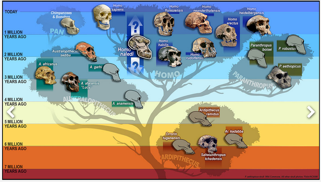
Discovery of Homo naledi adds a new branch to the human family tree

Skeletal fossil of the hand of Homo naledi (photo credit: John Hawks, UW–Madison)

An international research team has discovered a new species of a human relative, Homo naledi, uncovered in a cave outside of Johannesburg, South Africa. The discovery in late 2013 may shed light on the diversity of our genus and possibly its origin.

The team’s findings, which are published in two papers in the open-access journal eLife, were announced by South Africa’s University of the Witwatersrand, the National Geographic Society, and the South African National Research Foundation.

Homo naledi: A New Species on the Human Family Tree (illustration credit: S.V. Medaris/UW-Madison)

The authors describe Homo naledi as being similar in size and weight to a small modern human, with human-like hands and feet. The skull had a small braincase “similar in size to other early hominin species that lived between four million and two million years ago.”

The discovery indicates that H. naledi intentionally deposited bodies of its dead in a remote cave chamber — behaviors previously thought limited to humans.

This figure includes the 737 partial or complete anatomical elements of Homo naledi found (credit: Lee R. Berger et al./eLife)

Lee Berger, a research professor in the Evolutionary Studies Institute at the University of the Witwatersrand and a National Geographic Explorer-in-Residence, led the expeditions that recovered the fossils — more than 1,500 bones belonging to at least 15 individuals.

The National Geographic article “This Face Changes the Human Story. But How?” offers striking art and photography on this discovery.


University of Wisconsin-Madison | Meet our newest ancestor: Homo naledi


Abstract of Homo naledi, a new species of the genus Homo from the Dinaledi Chamber, South Africa
Homo naledi is a previously-unknown species of extinct hominin discovered within the Dinaledi Chamber of the Rising Star cave system, Cradle of Humankind, South Africa. This species is characterized by body mass and stature similar to small-bodied human populations but a small endocranial volume similar to australopiths. Cranial morphology of H. naledi is unique, but most similar to early Homo species including Homo erectusHomo habilis orHomo rudolfensis. While primitive, the dentition is generally small and simple in occlusal morphology. H. naledi has humanlike manipulatory adaptations of the hand and wrist. It also exhibits a humanlike foot and lower limb. These humanlike aspects are contrasted in the postcrania with a more primitive or australopith-like trunk, shoulder, pelvis and proximal femur. Representing at least 15 individuals with most skeletal elements repeated multiple times, this is the largest assemblage of a single species of hominins yet discovered in Africa.


Abstract of Geological and taphonomic context for the new hominin species Homo naledi from the Dinaledi Chamber, South Africa

We describe the physical context of the Dinaledi Chamber within the Rising Star cave, South Africa, which contains the fossils of Homo naledi. Approximately 1550 specimens of hominin remains have been recovered from at least 15 individuals, representing a small portion of the total fossil content. Macro-vertebrate fossils are exclusively H. naledi, and occur within clay-rich sediments derived from in situ weathering, and exogenous clay and silt, which entered the chamber through fractures that prevented passage of coarser-grained material. The chamber was always in the dark zone, and not accessible to non-hominins. Bone taphonomy indicates that hominin individuals reached the chamber complete, with disarticulation occurring during/after deposition. Hominins accumulated over time as older laminated mudstone units and sediment along the cave floor were eroded. Preliminary evidence is consistent with deliberate body disposal in a single location, by a hominin species other than Homo sapiens, at an as-yet unknown date.

The CRISPR controversy: faster, cheaper gene editing vs. bioethicists

Clustered regularly interspaced short palindromic repeats (CRISPRs) technology employs a guide RNA to direct the Cas9 enzyme (light blue) to a target DNA sequence. Once there, Cas9 will bind when it finds a protospacer-adjacent motif sequence (red) in the DNA and cut both strands, priming the gene sequence for editing. (credit: Adapted from OriGene Technologies)

Within the past few years, a new technology has made altering genes in plants and animals much easier than before. The tool, called CRISPR/Cas9 or just CRISPR, has spurred a flurry of research that could one day lead to hardier crops and livestock, as well as innovative biomedicines.

But along with potential benefits, it raises red flags, according to an open-access article in Chemical & Engineering News (C&EN), the weekly newsmagazine of the American Chemical Society.

Ann M. Thayer, a senior correspondent at C&EN, notes that scientists have long had the ability to remove, repair or insert genetic material in cells. But the process was time consuming and expensive. CRISPR (“clustered regularly interspaced short palinodromic repeats”) streamlines gene editing dramatically. Its simplicity has enabled far more scientists to get involved in such work. In a short time, they have now used CRISPR to edit genes in insects, plants, fish, rodents and monkeys.

The potential agricultural and medical applications that could result from the tool in the future have attracted the interest of venture capitalists and pharmaceutical companies, the article says. While it seems CRISPR work is moving full-steam ahead, a couple of recent developments could check its growth.

In April, Chinese scientists reported that they had attempted to alter a gene in nonviable human embryos. The announcement sparked bioethicists to call for a more cautious approach to gene editing. The other wrench in the system is an ongoing dispute over who should be awarded the patent for inventing CRISPR. Until these issues are resolved, some investors and researchers will opt to wait on the sidelines.


McGovern Institute for Brain Research at MIT | Genome Editing with CRISPR-Cas9

Magnetic solitons may lead to more energy-efficient computing

Schematic of the x-ray microscopy measurements. The x-ray spot size at the sample was 35 nm and the transmitted x-rays (from the zone plate) were detected by an avalanche photo diode. Images were recorded by raster scanning of the sample. (credit: R. Kukreja et al./Physics Review Letters)

A team of physicists has taken pictures of a theorized but previously undetected “magnetic soliton” that they believe could be an energy-efficient means to transfer data in future electronic devices.

The research, which appears in the journal Physical Review Letters, was conducted by scientists at New York University, Stanford University, and the SLAC National Accelerator Laboratory.

Harnessing solitons to transmit data

Illustration of a water soliton wave. The blue line represents carrier (energy source) waves, while the red line is the envelope. (credit: Wikimedia Commons)

Solitons (solitary waves) were theorized in the 1970s to occur in magnets. They form because of a delicate balance of magnetic forces — much like water waves can form a tsunami. These magnetic waves could potentially be harnessed to transmit data in magnetic circuits in a way that is far more energy-efficient than current methods that involve moving electrical charges, the researchers suggest.

That’s because solitons are stable objects that overcome resistance, or friction, as they move. By contrast, electrons, used to move data today, generate heat as they travel, due to resistance and thus require additional energy, such as from a battery, as they transport data to its destination.

The scientists made the discovery using x-ray microscopy at the Stanford Synchrotron Radiation Lightsource. They observed an abrupt onset of magnetic waves with a well-defined spatial profile that matched the predicted form of a solitary magnetic wave, or magnetic soliton.

“This is an exciting discovery because it shows that small magnetic waves — also known as spin-waves — can add up to a large … wave that can maintain its shape as it moves,” explains Andrew Kent, a professor of physics at NYU and the study’s senior author.

“Magnetism has been used for navigation for thousands of years and more recently to build generators, motors, and data storage devices,” adds co-author Hendrik Ohldag, a scientist at the Stanford Synchrotron Radiation Laboratory (SSRL), where the soliton was discovered. “However, magnetic elements were mostly viewed as static and uniform. To push the limits of energy efficiency in the future we need to understand better how magnetic devices behave on fast timescales at the nanoscale, which is why we are using this dedicated ultrafast x-ray microscope.”


Abstract of X-ray Detection of Transient Magnetic Moments Induced by a Spin Current in Cu

We have used a MHz lock-in x-ray spectromicroscopy technique to directly detect changes in magnetic moment of Cu due to spin injection from an adjacent Co layer. The elemental and chemical specificity of x rays allows us to distinguish two spin current induced effects. We detect the creation of transient magnetic moments of 3 × 10⁻⁵μB on Cu atoms within the bulk of the 28 nm thick Cu film due to spin accumulation. The moment value is compared to predictions by Mott’s two current model. We also observe that the hybridization induced existing magnetic moments at the Cu interface atoms are transiently increased by about 10% or 4 × 10⁻³μB per atom. This reveals the dominance of spin-torque alignment over Joule heat induced disorder of the interfacial Cu moments during current flow.

Why human genome editing research is essential

(credit: NIH)

Research involving editing the human genome, including research with human embryos, is essential to gain basic understanding of biology and germ cells and should be permitted, according to one of the first global meetings to debate the controversial new techniques.

The bold statement was published today (Thursday, Sept. 10) by the Hinxton Group, a global network of stem cell researchers, bioethicists, and experts on policy and scientific publishing, who met in Manchester, England, September 3–4.

Not ready for clinical applications

“We believe that while this technology has tremendous value to basic research and enormous potential for somatic clinical uses, it is not sufficiently developed to consider human genome editing for clinical reproductive purposes at this time,” the consensus statement reads.

Discussions at the meeting included the most contentious aspects of these new technologies — the implications for any children born with engineered genetic modifications, and also successive generations who would inherit those genetic changes, according to Debra Mathews, a member of the Hinxton Group steering committee.

“While there is controversy and deep moral disagreement about human germline genetic modification, what is needed is not to stop all discussion, debate and research, but rather to engage with the public, policymakers and the broader scientific community, and to weigh together the potential benefits and harms of human genome editing for research and human health,” says Mathews, the Assistant Director for Science Programs at the Johns Hopkins Berman Institute of Bioethics.

The consensus statement addresses these ethical concerns, with the group agreeing that, “given all safety, efficacy and governance needs are met, there may be morally acceptable uses of this technology in human reproduction, though further substantial discussion and debate will be required.”

Basic research with human embryos

In the meantime, knowledge gained through basic science research is essential to human understanding of both ourselves and other life, the group says. “Much of our knowledge of early development comes from studies of mouse embryos, yet it is becoming clear that gene activity and even some cell types are very different in human embryos.”

Genome editing techniques could be used to ask how cell types are specified in the early embryo and the nature and importance of the genes involved,” says Robin Lovell-Badge, a member of the Hinxton Group steering committee and Group Leader, and head of the Laboratory of Stem Cell Biology and Developmental Genetics, The Francis Crick Institute.

The statement emphasizes the importance of “meaningful and substantial public engagement” to decision-making about genome editing, stating that policy restraints on science should have justification that “that reaches beyond disagreements based solely on divergent moral convictions.”

“The relevant regulatory distinction should be not between using genome editing in somatic cells and using it in embryos, but between research and reproduction: whether those embryos are ever destined to be implanted, says Sarah Chan, another steering committee member and a Chancellor’s Fellow at the Usher Institute for Population Health Sciences and Informatics, University of Edinburgh.

“Restricting research because of concerns that reproductive application is premature and dangerous will ensure that it remains forever premature and dangerous, for want of better knowledge,” Chan says.

New video series ‘Beyond the Desktop’ explores potential of 3-D printing

A five-episode video series called Beyond the Desktop that explores how additive manufacturing could affect the fields of medicine, aerospace, space technology and more has been released by the Wilson Center’s Science and Technology Innovation Program (STIP). The first episode was posted yesterday (Sept. 9); a new episode will be released each Wednesday through early October.

“Desktop 3-D printing has received significant media coverage, but this hides the larger story happening in industry, where the technology will change everything from prototyping to the production of complex parts and the design of supply chains,” says David Rejeski, director of the Science and Technology Innovation Program at the Wilson Center and executive producer of the series.

The series looks at how doctors are already incorporating 3-D printing into their surgical work, how aerospace manufacturers are finding cost savings in using additive manufacturing to build critical parts, and how startups are using 3-D printing to enable longer supply chains into space.

Beyond the Desktop builds upon other STIP work focused on additive manufacturing. Last month, the program released the results of a workshop that examined the environmental and human health implication of additive manufacturing. Sponsored by the National Science Foundation, the workshop was conducted in conjunction with the Center for Manufacturing Innovation at the University of Florida.

Beyond the Desktop was filmed on location in California, Illinois, and Washington, DC in 2013–2015.


Wilson Center | Beyond the Desktop: The Potential of Additive Manufacturing (Episode 1)