First superconducting graphene created

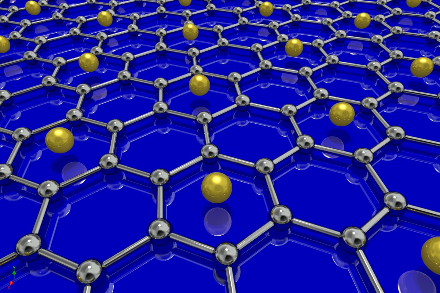
University of British Columbia physicists have created the first superconducting graphene sample by coating it with lithium atoms (yellow), shown in this illustration (credit: University of British Columbia)

University of British Columbia (UBC) physicists have created the first single-layer superconducting graphene sample by coating it with lithium atoms.

Although superconductivity has already been observed in layered bulk graphite, inducing superconductivity in single-layer graphene has until now eluded scientists.

“This first experimental realization of superconductivity in graphene promises to usher us in a new era of graphene electronics and nanoscale quantum devices,” says Andrea Damascelli, director of UBC’s Quantum Matter Institute and leading scientist of the Proceedings of the National Academy of Sciences study outlining the discovery. A superconductive wire would have zero resistance at ultra-low temperatures (at a critical temperature* of about 5.9K), so a current flowing through it would generate no heat.

Given the massive scientific and technological interest, the ability to induce superconductivity in single-layer graphene promises to have significant cross-disciplinary impacts, the researchers say.

To achieve this breakthrough, the researchers, which include colleagues at the Max Planck Institute for Solid State Research, prepared the lithium-decorated graphene in ultra-high vacuum conditions.

Scientists eventually hope to make very fast transistors, semiconductors, sensors, and transparent electrodes using graphene, a single layer of carbon atoms arranged in a honeycomb pattern.

* The temperature below which superconductivity appears.

UPDATE Sept. 14, 2015: critical temperature added.


Abstract of Evidence for superconductivity in Li-decorated monolayer graphene

Monolayer graphene exhibits many spectacular electronic properties, with superconductivity being arguably the most notable exception. It was theoretically proposed that superconductivity might be induced by enhancing the electron–phonon coupling through the decoration of graphene with an alkali adatom superlattice [Profeta G, Calandra M, Mauri F (2012) Nat Phys 8(2):131–134]. Although experiments have shown an adatom-induced enhancement of the electron–phonon coupling, superconductivity has never been observed. Using angle-resolved photoemission spectroscopy (ARPES), we show that lithium deposited on graphene at low temperature strongly modifies the phonon density of states, leading to an enhancement of the electron–phonon coupling of up to λ≃0.58. On part of the graphene-derived π∗-band Fermi surface, we then observe the opening of a Δ≃0.9-meV temperature-dependent pairing gap. This result suggests for the first time, to our knowledge, that Li-decorated monolayer graphene is indeed superconducting, with Tc≃5.9 K.

Functional carbon nanotube integrated circuits: a breakthrough

Atomic force micrograph of complementary single-wall carbon nanotubes in thin-film-transistor channel (credit: Michael L. Geier et al./Nature Nanotechnology)

Northwestern University engineers say that have finally found the key to practical use of carbon nanotubes (CNTs) in integrated circuits. Individual transistors made from CNTs are faster and more energy-efficient and reliable than those made from other materials.

The problem. But making the leap to wafer-scale integrated circuits (a microprocessor typically has a billion transistors) is a challenge. The process is incredibly expensive, often requiring billion-dollar cleanrooms to keep the delicate nano-sized components safe from the potentially damaging effects of air, water, and dust.

And researchers have struggled to create a carbon nanotube-based integrated circuit in which the transistors are spatially uniform across the material, which is needed for the overall system to work.

The solution. Now Hersam and his team have found a key to solving all these issues: newly developed encapsulation layers that protect carbon nanotubes from environmental degradation.

Dealing with environmental degradation

“One of the realities of a nanomaterial, such as a carbon nanotube, is that essentially all of its atoms are on the surface,” explained Northwestern Engineering’s Mark Hersam, the Walter P. Murphy Professor of Materials Science and Engineering. “So anything that touches the surface of these materials can influence their properties.

“If we made a series of transistors and left them out in the air, water and oxygen would stick to the surface of the nanotubes, degrading them over time. We thought that adding a protective encapsulation layer could arrest this degradation process to achieve substantially longer lifetimes.”*

To demonstrate proof of concept, Hersam developed nanotube-based static random-access memory (SRAM) circuits. SRAM is a key component of all microprocessors, often making up as much as 85 percent of the transistors in the central-processing unit in a common computer. To create the encapsulated carbon nanotubes, the team first deposited the carbon nanotubes from a solution previously developed in Hersam’s lab. Then they coated the tubes with their encapsulation layers.

Functional CNT-based SRAM memory circuits

Complementary single-wall carbon nanotube thin-film-transistor (SWCNT TFT) structures. (A) Optical micrographs of the fabricated device with channel width of 150 μm and length of 50 μm (inset) and an array of SWCNT TFTs (scale bar: 1 mm). (B) Schematic cross-section of a SWCNT TFT. (C) Atomic force micrograph of the SWCNTs in the TFT channel with a linear density of ~10 SWCNTs/μm (Height color bar: 0 to 15 nm). (credit: Michael L. Geier et al./Nature Nanotechnology)

Using the encapsulated carbon nanotubes, Hersam’s team successfully designed and fabricated arrays of working SRAM circuits. Not only did the encapsulation layers protect the sensitive device from the environment, but they improved spatial uniformity among individual transistors across the wafer. While Hersam’s integrated circuits demonstrated a long lifetime, transistors that were deposited from the same solution but not coated degraded within hours.

“After we’ve made the devices, we can leave them out in air with no further precautions,” Hersam said. “We don’t need to put them in a vacuum chamber or controlled environment. Other researchers have made similar devices but immediately had to put them in a vacuum chamber or inert environment to keep them stable. That’s obviously not going to work in a real-world situation.”

Implications for portable/wearable electronics

These features, when combined with recent advances in flexible and printed electronics have potentially wide-ranging implications for high-performance portable and wearable electronics, the researchers suggest in the paper.

Flexible carbon nanotube-based transistors could replace rigid silicon to enable wearable electronics, Hersam says. The cheaper manufacturing method also opens doors for smart cards — credit cards embedded with personal information to reduce the likelihood of fraud.

“Smart cards are only realistic if they can be realized using extremely low-cost manufacturing,” he said. “Because our solution-processed carbon nanotubes are compatible with scalable and inexpensive printing methods, our results could enable smart cards and related printed electronics applications.”

The research appeared online in Nature Nanotechology on September 7. It was supported by the Office of Naval Research and the National Science Foundation.

* Hersam compares his solution to one currently used for organic light-emitting diodes (LEDs), which experienced similar problems after they were first realized. Many people assumed that organic LEDs would have no future because they degraded in air. After researchers developed an encapsulation layer for the material, organic LEDs are now used in many commercial applications, including displays for smartphones, car radios, televisions, and digital cameras. Made from polymers and inorganic oxides, Hersam’s encapsulation layer is based on the same idea but tailored for carbon nanotubes.


Abstract of Solution-processed carbon nanotube thin-film complementary static random access memory

Over the past two decades, extensive research on single-walled carbon nanotubes (SWCNTs) has elucidated their many extraordinary properties, making them one of the most promising candidates for solution-processable, high-performance integrated circuits. In particular, advances in the enrichment of high-purity semiconducting SWCNTs have enabled recent circuit demonstrations including synchronous digital logic, flexible electronics and high-frequency applications. However, due to the stringent requirements of the transistors used in complementary metal–oxide–semiconductor (CMOS) logic as well as the absence of sufficiently stable and spatially homogeneous SWCNT thin-film transistors, the development of large-scale SWCNT CMOS integrated circuits has been limited in both complexity and functionality. Here, we demonstrate the stable and uniform electronic performance of complementary p-type and n-type SWCNT thin-film transistors by controlling adsorbed atmospheric dopants and incorporating robust encapsulation layers. Based on these complementary SWCNT thin-film transistors, we simulate, design and fabricate arrays of low-power static random access memory circuits, achieving large-scale integration for the first time based on solution-processed semiconductors.
An experimental ultrafast optical transistor based on a silicon nanoparticle

An illustration of a silicon nanoparticle switching between modes, depending on the intensity of a laser pulse (credit: Nano Letters)

Russian physicists have invented an optical version of a transistor, based on a silicon nanoparticle. The research could lead to optical computers in the future.

Current computers are limited by the time needed to trigger a transistor — usually around 0.1 to 1 nanosecond (10−9 of a second). An optical transistor could work up to 1000 times faster — at picoseconds (10−12 of a second), the researchers explain.

In the study, a group of Russian scientists from ITMO University, Lebedev Physical Institute and Academic University in Saint Petersburg created a new approach to designing optical transistors, based on a prototype using only one silicon nanoparticle.

They achieved this by irradiating the silicon nanoparticle with an intense, ultrashort laser pulse*, which caused the nanoparticle to switch the direction in which incident light was scattered. The next step is to introduce introduce a signal beam.

The study was published in the scientific journal Nano Letters.

* The laser acts as a control beam, providing ultrafast photoexcitation of dense and rapidly recombining electron-hole plasma whose presence changes the dielectric permittivity of silicon for a few picoseconds. This abrupt change in the optical properties of the nanoparticle allowed for controlling the direction in which incident light was scattered.


Abstract of Tuning of Magnetic Optical Response in a Dielectric Nanoparticle by Ultrafast Photoexcitation of Dense Electron–Hole Plasma

We propose a novel approach for efficient tuning of optical properties of a high refractive index subwavelength nanoparticle with a magnetic Mie-type resonance by means of femtosecond laser irradiation. This concept is based on ultrafast photoinjection of dense (>1020 cm–3) electron–hole plasma within such nanoparticle, drastically changing its transient dielectric permittivity. This allows manipulation by both electric and magnetic nanoparticle responses, resulting in dramatic changes of its scattering diagram and scattering cross section. We experimentally demonstrate 20% tuning of reflectance of a single silicon nanoparticle by femtosecond laser pulses with wavelength in the vicinity of the magnetic dipole resonance. Such a single-particle nanodevice enables designing of fast and ultracompact optical switchers and modulators.

‘I’ve seen the future, and it’s …. paper’

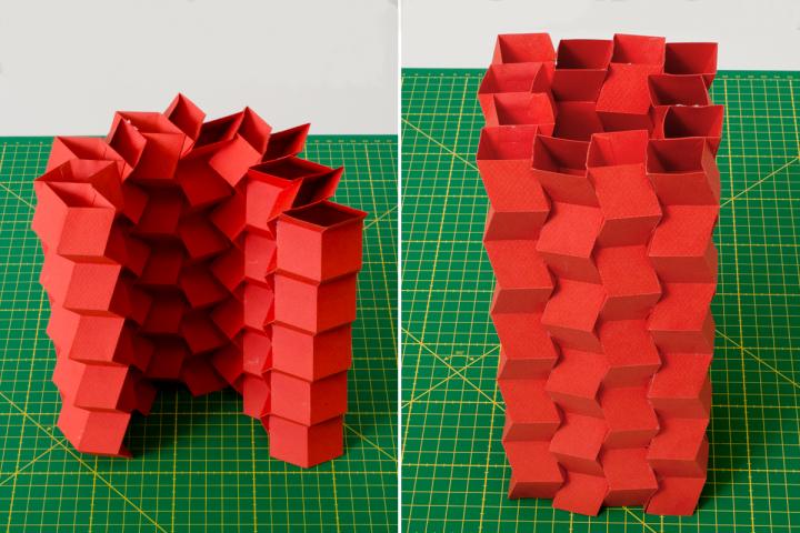
Interlocking origami zigzag paper tubes can be configured to build a variety of structures that have stiffness and function, but can fold compactly for storage or shipping. (credit: Rob Felt)

A new origami “zippered tube” design that makes paper-based (or other thin materials) structures stiff enough to hold weight, yet can fold flat for easy shipping and storage could transform structures ranging from microscopic robots to furniture and even buildings.

That’s what researchers from the University of Illinois at Urbana-Champaign, the Georgia Institute of Technology, and the University of Tokyo suggest in a Proceedings of the National Academy of Sciences paper.

Such origami structures could include a robotic arm that reaches out and scrunches up, a construction crane that folds to pick up or deliver a load,  furniture, and quick-assembling emergency shelters, bridges — and other infrastructure used in the wake of a natural disaster.

Pop-up buildings?

The researchers use a particular origami technique called Miura-ori folding: They make precise, zigzag-folded strips of paper, then glue two strips together to make a tube. While the single strip of paper is highly flexible, the tube is stiffer and does not fold in as many directions.

Interlocking two tubes in zipper-like fashion made them much stiffer and harder to twist or bend, they found. The structure folds up flat, yet rapidly and easily expands to the rigid tube configuration.

The zipper configuration works even with tubes that have different angles of folding. By combining tubes with different geometries, the researchers can make many different three-dimensional structures, such as a bridge, a canopy, or a tower.

Origami “zipper tubes” — interlocking zigzag paper tubes — can be configured to build a variety of structures that have stiffness and function, but can fold compactly for storage or shipping (credit: L. Brian Stauffer)

Transformable structures

“The ability to change functionality in real time is a real advantage in origami,” said Georgia Tech professor Glaucio Paulino. “By having these transformable structures, you can change their functionality and make them adaptable. They are reconfigurable. You can change the material characteristics: You can make them stiffer or softer depending on the intended use.”

The team uses paper prototypes to demonstrate how a thin, flexible sheet can be folded into functional structures, but their techniques could be applied to other thin materials, according to the researchers. Larger-scale applications could combine metal or plastic panels with hinges.

Next, the researchers plan to explore new combinations of tubes with different folding angles to build new structures. They also hope to apply their techniques to other materials and explore applications from large-scale construction to microscopic structures for biomedical devices or robotics.

“All of these ideas apply from the nanoscale and microscale up to large scales and even structures that NASA would deploy into space,” Paulino said. “Depending on your interest, the applications are endless. We have just scratched the surface. Once you have a powerful concept, which we think the zipper coupling is, you can explore applications in many different areas.”


Abstract of Origami tubes assembled into stiff, yet reconfigurable structures and metamaterials

Thin sheets have long been known to experience an increase in stiffness when they are bent, buckled, or assembled into smaller interlocking structures. We introduce a unique orientation for coupling rigidly foldable origami tubes in a “zipper” fashion that substantially increases the system stiffness and permits only one flexible deformation mode through which the structure can deploy. The flexible deployment of the tubular structures is permitted by localized bending of the origami along prescribed fold lines. All other deformation modes, such as global bending and twisting of the structural system, are substantially stiffer because the tubular assemblages are overconstrained and the thin sheets become engaged in tension and compression. The zipper-coupled tubes yield an unusually large eigenvalue bandgap that represents the unique difference in stiffness between deformation modes. Furthermore, we couple compatible origami tubes into a variety of cellular assemblages that can enhance mechanical characteristics and geometric versatility, leading to a potential design paradigm for structures and metamaterials that can be deployed, stiffened, and tuned. The enhanced mechanical properties, versatility, and adaptivity of these thin sheet systems can provide practical solutions of varying geometric scales in science and engineering.

Lipid DNA origami may lead to advanced future nanomachines

Using a double layer of lipids facilitates assembly of DNA origami nanostructures, bringing us one step closer to future DNA nanomachines, as in this artist’s impression (credit: Kyoto University’s Institute for Integrated Cell-Material Sciences)

Kyoto University scientists in Japan have developed a method for creating larger 2-D self-assembling DNA origami* nanostructures.

Current DNA origami methods can create extremely small two- and three-dimensional shapes that could be used as construction material to build nanodevices, such as nanomotors, in the future for targeted drug delivery inside the body, for example. KurzweilAI recently covered advanced methods developed by Brookhaven National Laboratory and  Arizona State University’s Biodesign Institute.

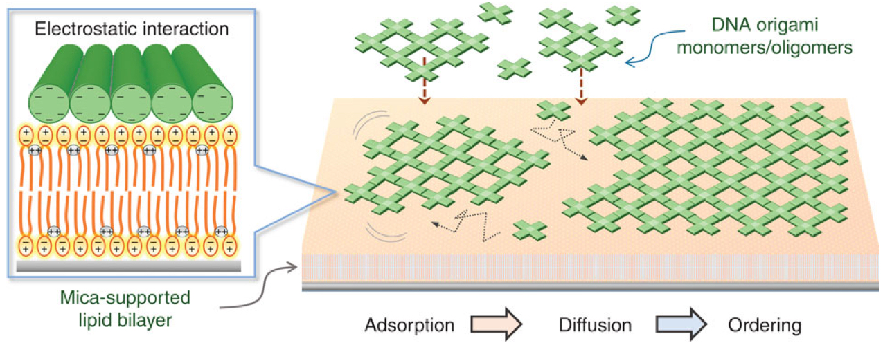
Lipid bilayer allows DNA origami structures to easily self-assemble into 2-D nanostructures (credit: Yuki Suzuki et al./Nature Communications)

Unlike those rigid structures, the Kyoto scientists used a double layer of lipids (fats) containing both a positive and a negative charge. That caused the DNA origami structures to be absorbed onto the lipid layer via electrostatic interaction. The weak bond between the origami structures and the lipid layer allowed them to move more freely than in other approaches, facilitating their interaction with one another and allowing them to self-assemble and form larger structures.

“We anticipate that our approach will further expand the potential applications of DNA origami structures and their assemblies in the fields of nanotechnology, biophysics, and synthetic biology,” says chemical biologist Professor Hiroshi Sugiyama from Kyoto University’s Institute for Integrated Cell-Material Sciences (iCeMS).

The study was published in an open-access paper in Nature Communications on August 27, 2015.

* The technique of DNA origami capitalizes on the simple base-pairing properties of DNA, a molecule built from the four nucleotides Adenine (A)Thymine (T)Cytosine (C) and Guanine (G). The rules of the game are simple: A’s always pair with T’s and C’s with G’s. Using this abbreviated vocabulary, the myriad body plans of all living organisms are constructed; though duplicating even Nature’s simpler designs has required great ingenuity.

The basic idea of DNA origami is to use a length of single-stranded DNA as a scaffold for the desired shape. Base-pairing of complementary nucleotides causes the form to fold and self-assemble. The process is guided by the addition of shorter “staple strands,” which act to help fold the scaffold and to hold the resulting structure together. Various imaging technologies are used to observe the tiny structures, including fluorescence-, electron- and atomic-force microscopy.


Abstract of Lipid-bilayer-assisted two-dimensional self-assembly of DNA origami nanostructures

Self-assembly is a ubiquitous approach to the design and fabrication of novel supermolecular architectures. Here we report a strategy termed ‘lipid-bilayer-assisted self-assembly’ that is used to assemble DNA origami nanostructures into two-dimensional lattices. DNA origami structures are electrostatically adsorbed onto a mica-supported zwitterionic lipid bilayer in the presence of divalent cations. We demonstrate that the bilayer-adsorbed origami units are mobile on the surface and self-assembled into large micrometre-sized lattices in their lateral dimensions. Using high-speed atomic force microscopy imaging, a variety of dynamic processes involved in the formation of the lattice, such as fusion, reorganization and defect filling, are successfully visualized. The surface modifiability of the assembled lattice is also demonstrated by in situ decoration with streptavidin molecules. Our approach provides a new strategy for preparing versatile scaffolds for nanofabrication and paves the way for organizing functional nanodevices in a micrometer space.

First known magnetic wormhole created

(Left) 3-D diagram of the magnetic wormhole shows how the magnetic field lines (in red) leaving a magnet on the right side of the sphere pass through the wormhole. (Right) As seen by a magnet, the magnetic field seems to disappear on the right side of the sphere only to reappear on the left in the form of a magnetic monopole. (credit: Jordi Prat-Camps/Universitat Autònoma de Barcelona)

A wormhole* that can connect two regions of space magnetically has been created in the laboratory and experimentally demonstrated by physicists at Universitat Autònoma de Barcelona in Spain.

This is not a wormhole in space, as in the movie Interstellar. It’s a special design that transfers a magnetic field from one location in space to another in such a way that the process is magnetically undetectable and invisible (only visible by light). This is explained in the diagrams above.

The researchers used metamaterials and metasurfaces to build the tunnel experimentally. The magnetic field from a source, such as a magnet or an electromagnet, appears at the other end of the wormhole as an isolated magnetic monopole (a magnet with only one pole, whether north or south, which does not exist in nature).

That causes the magnetic field to appear to magically travel from one location to another through a dimension that appears to (or actually?) lies outside the conventional three dimensions.

How to build a wormhole

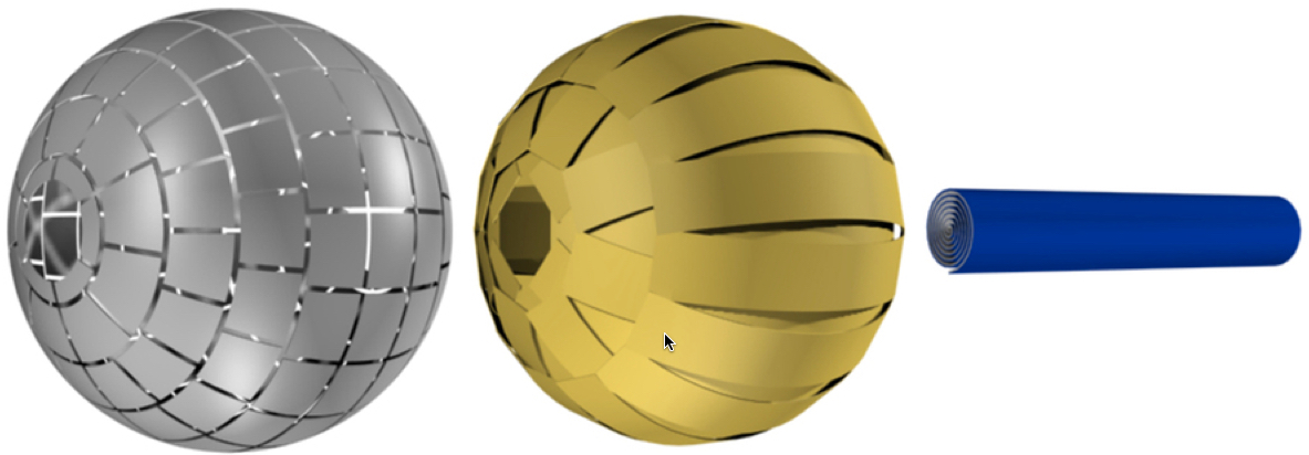
The magnetic wormhole device is composed of (from left to right) an outer spherical ferromagnetic metasurface, an inner spherical superconducting layer, and inside that, an inner spirally wound ferromagnetic sheet (credit: (credit: Jordi Prat-Camps/Universitat Autònoma de Barcelona)

To create the wormhole used in this experiment, the researchers designed a sphere made of three layers: an external layer with a ferromagnetic (as in a standard iron magnet) surface, a second inner layer made of superconducting material, and a ferromagnetic sheet rolled into a cylinder that crosses the sphere from one end to the other and conducts the magnetic field.

The magnetic wormhole is analogous to a gravitational wormhole — it “changes the topology of space, as if the inner region has been magnetically erased from space,” explains Àlvar Sánchez, the lead researcher.

Practical applications

The study was published in an open-access paper in Scientific Reports, but the researchers first published the fundamental concept in a paper in Physical Review Letters, where they described it as a “magnetic hose.”

Experimental magnetic wormhole (credit: Jordi Prat-Camps/Universitat Autònoma de Barcelona)

The researchers built a magnetic “hose” capable of channeling a magnetic field from a source to a distance more than 10 centimeters away. (However, that version was detectable magnetically.)

As Steven Anlage, a professor of Physics at the University of Maryland, explains in this open-access article in the journal Physics, channeling magnetic fields could improve the spatial resolution of magnetic-field images, for example.

“Another application would be magnetic resonance imaging, in which the patient and superconducting magnet required to generate the magnetic field could be physically separated, and the intense magnetic field could be applied locally to the patient” (instead of having to enter an MRI machine).

Or it could allow MRI images of different parts of the body to be obtained simultaneously.

There may be other possible uses. Any ideas? Please comment below.

* Wormholes are cosmic tunnels that can connect two distant regions of the universe, popularized by science fiction like Stargate, Star Trek or, more recently, Interstellar. Using present-day technology, it would be impossible to create a gravitational wormhole because the field would have to be manipulated with huge amounts of gravitational energy, which no one yet knows how to generate. In electromagnetism, however, advances in metamaterials and invisibility have allowed researchers to put forward several designs to achieve this.


Abstract of A Magnetic Wormhole

Wormholes are fascinating cosmological objects that can connect two distant regions of the universe. Because of their intriguing nature, constructing a wormhole in a lab seems a formidable task. A theoretical proposal by Greenleaf et al. presented a strategy to build a wormhole for electromagnetic waves. Based on metamaterials, it could allow electromagnetic wave propagation between two points in space through an invisible tunnel. However, an actual realization has not been possible until now. Here we construct and experimentally demonstrate a magnetostatic wormhole. Using magnetic metamaterials and metasurfaces, our wormhole transfers the magnetic field from one point in space to another through a path that is magnetically undetectable. We experimentally show that the magnetic field from a source at one end of the wormhole appears at the other end as an isolated magnetic monopolar field, creating the illusion of a magnetic field propagating through a tunnel outside the 3D space. Practical applications of the results can be envisaged, including medical techniques based on magnetism.

New laser design could dramatically shrink autonomous-vehicle 3-D laser-ranging systems

This self-sweeping laser couples an optical field with the mechanical motion of a high-contrast grating (HCG) mirror. The HCG mirror is supported by mechanical springs connected to layers of semiconductor material. The red layer represents the laser’s gain (for light amplification), and the blue layers form the system’s second mirror. The force of the light causes the top mirror to vibrate at high speed. The vibration allows the laser to automatically change color as it scans. (credit: Weijian Yang)

UC Berkeley engineers have invented a new laser-ranging system that can reduce the power consumption, size, weight and cost of LIDAR (light detection and ranging, aka “light radar”), which is used in self-driving vehicles* to determine the distance to an object, and in real-time image capture for 3D videos.

“The advance could shrink components that now take up the space of a shoebox down to something compact and lightweight enough for smartphones or small UAVs [unmanned aerial vehicles],” said Connie Chang-Hasnain, a professor of electrical engineering and computer sciences at UC Berkeley.

Google self-driving cars use LIDAR (shown on top) to determine the distance of objects around them (credit: Google)

A system called optical coherence tomography (OCT) used in 3D medical imaging (especially for the retina) would also benefit.

A minaturized 3-D laser-mirror system

A team used a novel concept to automate the way a light source changes its wavelength as it sweeps the surrounding landscape, as reported in an open-access paper in the journal Scientific Reports, published Thursday, Sept. 3.

In both applications, as the laser moves along, it must continuously change its frequency so that it can calculate the difference between the incoming, reflected light and the outgoing light. To change the frequency, at least one of the two mirrors in the laser cavity must move precisely.

“The mechanisms needed to control the mirrors are a part of what makes current LIDAR and OCT systems bulky, power-hungry, slow and complex,” study lead author Weijian Yang explained. “The faster the system must perform — such as in self-driving vehicles that must avoid collisions — the more power it needs.”

The novelty of the new design is that they have integrated the semiconductor laser with the mirror. That means a laser can be as small as a few hundred micrometers square, powered by an AA battery.

The study authors said the next stage of the research will be to incorporate this new laser design in current LIDAR or OCT systems and demonstrate its application in 3-D video imaging.

A U.S. Department of Defense National Security Science and Engineering Faculty Fellowship helped support this work.

* Google’s robotic cars have about $150,000 in equipment including a $70,000 LIDAR system. The range finder mounted on the top is a Velodyne 64-beam laser. This laser allows the vehicle to generate a detailed 3D map of its environment. The car then takes these generated maps and combines them with high-resolution maps of the world, producing different types of data models that allow it to drive itself. — “Google driverless car,” Wikipedia


Abstract of Laser optomechanics

Cavity optomechanics explores the interaction between optical field and mechanical motion. So far, this interaction has relied on the detuning between a passive optical resonator and an external pump laser. Here, we report a new scheme with mutual coupling between a mechanical oscillator supporting the mirror of a laser and the optical field generated by the laser itself. The optically active cavity greatly enhances the light-matter energy transfer. In this work, we use an electrically-pumped vertical-cavity surface-emitting laser (VCSEL) with an ultra-light-weight (130 pg) high-contrast-grating (HCG) mirror, whose reflectivity spectrum is designed to facilitate strong optomechanical coupling, to demonstrate optomechanically-induced regenerative oscillation of the laser optomechanical cavity. We observe >550 nm self-oscillation amplitude of the micromechanical oscillator, two to three orders of magnitude larger than typical, and correspondingly a 23 nm laser wavelength sweep. In addition to its immediate applications as a high-speed wavelength-swept source, this scheme also offers a new approach for integrated on-chip sensors.

Toyota invests $50 million in intelligent vehicle technology at Stanford, MIT AI research centers

MIT’s iconic Stata Center, which houses the Computer Science and Artificial Intelligence Laboratory (credit: MIT)

Toyota Motor Corporation (TMC) announced today (Fri. Sept. 4) that it will be investing approximately $50 million over the next five years to establish joint research centers at the Stanford Artificial Intelligence Lab (SAIL) and MIT’s Computer Science and Artificial Intelligence Laboratory (CSAIL).

Toyota also said Dr. Gill Pratt, former Program Manager at DARPA and leader of its recent Robotics Challenge, has joined Toyota to direct and accelerate these research activities and their application to intelligent vehicles and robotics.

Rather than fully autonomous vehicles (as in Google’s research), the program will initially focus on the acceleration of intelligent vehicle technology to help eliminate traffic casualties*, with the ultimate goal of helping improve quality of life through enhanced mobility and robotics, according to Kiyotaka Ise, who heads R&D at Toyota.

Specific research areas will include “improving the ability of intelligent vehicle technologies to recognize objects around the vehicle in diverse environments, provide elevated judgment of surrounding conditions, and safely collaborate with vehicle occupants, other vehicles, and pedestrians,” Pratt added. “The joint research will also look at applications of the same technology to human-interactive robotics and information service.”

“[The car] must ensure that it does no harm, not only some of the time, but almost all of the time,” said Pratt.

MIT research

Research at MIT, led by CSAIL director Professor Daniela Rus, will “develop advanced architectures that allow cars to better perceive and navigate their surroundings,” eventually developing a vehicle “incapable of getting into a collision.”

CSAIL researchers plan to explore an approach in which the human driver pays attention at all times, with an autonomous system that is there to jump in to save the driver in the event of an unavoidable accident. That will involve areas from computer vision and perception to planning and control to decision-making.

Rus envisions creating a system that could “prevent collisions and also provide drivers with assistance navigating tricky situations; support a tired driver by watching for unexpected dangers and diversions; and even offer helpful tips such as letting the driver know she is out of milk at home and planning a new route home that allows the driver to swing by the grocery store.”

Research at the new center will also include building new tools for collecting and analyzing navigation data, with the goal of learning from human driving; creating perception and decision-making systems for safe navigation; developing predictive models that can anticipate the behavior of humans, vehicles, and the larger environment; inventing state-of-the-art tools to handle congestion and high-speed driving in challenging situations including adverse weather; improving machine-vision algorithms used to detect and classify objects; and creating more intelligent user interfaces.

Stanford research

Led by Associate Professor Fei-Fei Li, the new SAIL-Toyota Center for AI Research will focus on teaching computers to see and make critical decisions about how to interact with the world.

Early on, the new effort will focus on AI-assisted driving to avoid automobile-related accidents. Li, a world-renowned expert in computer vision, said that Stanford will tackle the problem by addressing four main challenges of making a computer think like a person: perception, learning, reasoning, and interaction.

Stanford’s computer scientists will train computers to recognize objects and speech as well as data, and then use machine learning and statistical modeling to extract the meaningful data points — for instance, a swerving car versus a parked one. Other researchers will teach the AI platform to look at this critical data set and plot the safest driving action.

The first cars with AI technology will work as partners with the driver to make safe decisions, Li said, so devising ways to carefully and comfortably share control between the human and the computer will be instrumental in this technology gaining the public’s trust.

* The World Health Organization estimates that 3,400 people die each day from traffic-related accidents.

A user-friendly 3-D printing interface for customizing designs

A new browser-based interface for design novices allows a wide range of modifications to a basic design — such as a toy car — that are guaranteed to be both structurally stable and printable on a 3-D printer. (credit: the researchers, edited by MIT News)

Researchers at MIT and the Interdisciplinary Center Herzliya in Israel have developed a system that automatically turns CAD files into visual models that users can modify in real time, simply by moving virtual sliders on a Web page. Once the design meets their specifications, they can hit the print button to send it to a 3-D printer.

Currently, 3-D printing an object from any but the simplest designs requires expertise with computer-aided design (CAD) applications. Even for the experts, the design process is immensely time-consuming.

“We envision a world where everything you buy can potentially be customized,” says Masha Shugrina, an MIT graduate student in computer science and engineering and one of the new system’s designers.

The researchers presented their new system, dubbed “Fab Forms,” at the Association for Computing Machinery’s Siggraph conference in August.

How Fab Forms works

Fab Forms begins with a design created by a seasoned CAD user. It then sweeps through a wide range of values for the design’s parameters — the numbers that a CAD user would typically change by hand — calculating the resulting geometries and storing them in a database.

For each of those geometries, the system also runs a battery of tests, specified by the designer, and it again stores the results.

An automatically created Web App using Fab Form (credit: Maria Shugrina et al.)

Finally, the system generates a user interface, a Web page that can be opened in an ordinary browser. The interface consists of a central window, which displays a 3-D model of an object, and a group of sliders, which vary the parameters of the object’s design. The system automatically weeds out all the parameter values that lead to unprintable or unstable designs, so the sliders are restricted to valid designs.

Moving one of the sliders — changing the height of the shoe’s heel, say, or the width of the mug’s base — sweeps through visual depictions of the associated geometries, presenting in real time what would take hours to calculate with a CAD program. “The sample density is high enough that it looks continuous to the user,” Matusik says.

If, however, a particularly sharp-eyed user wanted a value for a parameter that fell between two of the samples stored in the database, the system can call up the CAD program, calculate the associated geometry, and then run tests on it. That might take several minutes, but at that point, the user will have a good idea of what the final design should look like.


Abstract of Fab Forms: Customizable Objects for Fabrication with Validity and Geometry Caching

We address the problem of allowing casual users to customize para metric models while maintaining their valid state as 3D-printable functional objects. We define Fab Form as any design representation that lends itself to interactive customization by a novice user, while remaining valid and manufacturable. We propose a method to achieve these Fab Form requirements for general parametric designs tagged with a general set of automated validity tests and a small number of parameters exposed to the casual user. Our solution separates Fab Form evaluation into a precomputation stage and a runtime stage. Parts of the geometry and design validity (such as manufacturability) are evaluated and stored in the precomputation stage by adaptively sampling the design space. At runtime the remainder of the evaluation is performed. This allows interactive navigation in the valid regions of the design space using an automatically generated Web user interface (UI). We evaluate our approach by converting several parametric models into corresponding Fab Forms.

The Holy Grail: Machine Learning + Extreme Robotics

Two experts on robotics and machine learning will reveal breakthrough developments in humanlike robots and machine learning at the annual SXSW conference in Austin next March, in a proposed* panel called “The Holy Grail: Machine Learning + Extreme Robotics.”

Participants will interact with Hanson Robotics’ forthcoming state-of-the-art female Sophia robot as a participant on the panel as she spontaneously tracks human faces, listens to speech, and generates a natural-language response while participating in dialogue about the potential of genius machines.

This conversation on the future of advanced robotics combined with machine learning and cognitive science will feature visionary Hanson Robotics founder/CEO David Hanson and Microsoft executive Jim Kankanias, who heads Program Management for Information Management and Machine Learning in the Cloud + Enterprise Division at Microsoft. The panel will be moderated by Hanson Robotics consultant Eric Shuss.

Stay tuned here for updates.

* Contingent on getting enough votes by end of day Friday, Sept. 4 (cast your vote here — requires registration).