Discovering new drugs and materials by ‘touching’ molecules in virtual reality

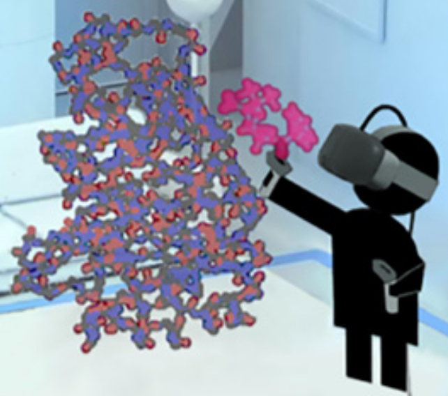
To figure out how to block a bacteria’s attempt to create multi-resistance to antibiotics, a researcher grabs a simulated ligand (binding molecule) — a type of penicillin called benzylpenicillin (red) — and interactively guides that molecule to dock within a larger enzyme molecule (blue-orange) called β-lactamase, which is produced by bacteria in an attempt to disable penicillin (making a patient resistant to a class of antibiotics called β-lactam). (credit: University of Bristol)

University of Bristol researchers, in collaboration with developers at Bristol based start-up Interactive Scientific, Oracle Corporation and a joint team of computer science and chemistry researchers, have designed and tested a new virtual reality (VR) cloud-based system intended to allow researchers to reach out and “touch” molecules as they move — folding them, knotting them, plucking them, and changing their shape to test how the molecules interact. The virtual reality cloud based system, called Nano Simbox, is the proprietary technology of Interactive Scientific, who collaborated with the University of Bristol to do the testing. Using an HTC Vive virtual-reality device, it could lead to creating new drugs and materials and improving the teaching of chemistry.

More broadly, the goal is to accelerate progress in nanoscale molecular engineering areas that include conformational mapping, drug development, synthetic biology, and catalyst design.

Real-time collaboration via the cloud

Two users passing a fullerene (C60) molecule back and forth in real time over a cloud-based network. The researchers are each wearing a VR head-mounted display (HMD) and holding two small wireless controllers that function as atomic “tweezers” to manipulate the real-time molecular dynamic of the C60 molecule. Each user’s position is determined using a real-time optical tracking system composed of synchronized infrared light sources, running locally on a GPU-accelerated computer. (credit: University of Bristol)

The multi-user system, developed by developed by a team led by University of Bristol chemists and computer scientists, uses an “interactive molecular dynamics virtual reality” (iMD VR) app that allows users to visualize and sample (with atomic-level precision) the structures and dynamics of complex molecular structures “on the fly” and to interact with other users in the same virtual environment.

Because each VR client has access to global position data of all other users, any user can see through his/her headset a co-located visual representation of all other users at the same time. So far, the system has uniquely allowed for simultaneously co-locating six users in the same room within the same simulation.

Testing on challenging molecular tasks

The team designed a series of molecular tasks for testing, using traditional mouse, keyboard, and touchscreens compared to virtual reality. The tasks included threading a small molecule through a nanotube, changing the screw-sense of a small organic helix, and tying a small string-like protein into a simple knot, and a variety of dynamic molecular problems, such as binding drugs to its target, protein folding, and chemical reactions. The researchers found that for complex 3D tasks, VR offers a significant advantage over current methods. For example, participants were ten times more likely to succeed in difficult tasks such as molecular knot tying.

Anyone can try out the tasks described in the open-access paper by downloading the software and launching their own cloud-hosted session.


David Glowacki | This video, made by University of Bristol PhD student Helen M. Deeks, shows the actions she took using a wireless set of “atomic tweezers” (using the HTC Vive) to interactively dock a single benzylpenicillin drug molecule into the active site of the β-lactamase enzyme. 


David Glowacki | The video shows the cloud-mounted virtual reality framework, with several different views overlaid to give a sense of how the interaction works. The video outlines the four different parts of the user studies: (1) manipulation of buckminsterfullerene, enabling users to familarize themselves with the interactive controls; (2) threading a methane molecule through a nanotube; (3) changing the screw-sense of a helicene molecule; and (4) tying a trefoil knot in 17-Alanine.

Ref: Science Advances (open-access). Source: University of Bristol.

IBM researchers use analog memory to train deep neural networks faster and more efficiently

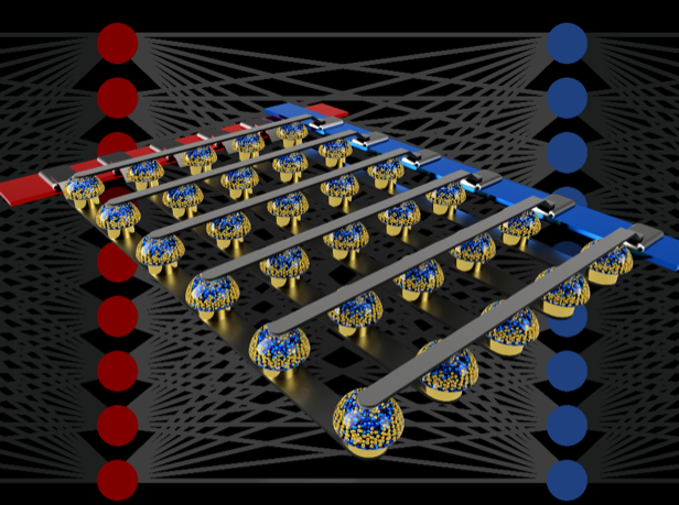
Crossbar arrays of non-volatile memories can accelerate the training of neural networks by performing computation at the actual location of the data. (credit: IBM Research)

Imagine advanced artificial intelligence (AI) running on your smartphone — instantly presenting the information that’s relevant to you in real time. Or a supercomputer that requires hundreds of times less energy.

The IBM Research AI team has demonstrated a new approach that they believe is a major step toward those scenarios.

Deep neural networks normally require fast, powerful graphical processing unit (GPU) hardware accelerators to support the needed high speed and computational accuracy — such as the GPU devices used in the just-announced Summit supercomputer. But GPUs are highly energy-intensive, making their use expensive and limiting their future growth, the researchers explain in a recent paper published in Nature.

Analog memory replaces software, overcoming the “von Neumann bottleneck”

Instead, the IBM researchers used large arrays of non-volatile analog memory devices (which use continuously variable signals rather than binary 0s and 1s) to perform computations. Those arrays allowed the researchers to create, in hardware, the same scale and precision of AI calculations that are achieved by more energy-intensive systems in software, but running hundreds of times faster and at hundreds of times lower power — without sacrificing the ability to create deep learning systems.*

The trick was to replace conventional von Neumann architecture, which is “constrained by the time and energy spent moving data back and forth between the memory and the processor (the ‘von Neumann bottleneck’),” the researchers explain in the paper. “By contrast, in a non-von Neumann scheme, computing is done at the location of the data [in memory], with the strengths of the synaptic connections (the ‘weights’) stored and adjusted directly in memory.

“Delivering the future of AI will require vastly expanding the scale of AI calculations,” they note. “Instead of shipping digital data on long journeys between digital memory chips and processing chips, we can perform all of the computation inside the analog memory chip. We believe this is a major step on the path to the kind of hardware accelerators necessary for the next AI breakthroughs.”**

Given these encouraging results, the IBM researchers have already started exploring the design of prototype hardware accelerator chips, as part of an IBM Research Frontiers Institute project, they said.

Ref.: Nature. Source: IBM Research

 * “From these early design efforts, we were able to provide, as part of our Nature paper, initial estimates for the potential of such [non-volatile memory]-based chips for training fully-connected layers, in terms of the computational energy efficiency (28,065 GOP/sec//W) and throughput-per-area (3.6 TOP/sec/mm2). These values exceed the specifications of today’s GPUs by two orders of magnitude. Furthermore, fully-connected layers are a type of neural network layer for which actual GPU performance frequently falls well below the rated specifications. … Analog non-volatile memories can efficiently accelerate at the heart of many recent AI advances. These memories allow the “multiply-accumulate” operations used throughout these algorithms to be parallelized in the analog domain, at the location of weight data, using underlying physics. Instead of large circuits to multiply and add digital numbers together, we simply pass a small current through a resistor into a wire, and then connect many such wires together to let the currents build up. This lets us perform many calculations at the same time, rather than one after the other.

** “By combining long-term storage in phase-change memory (PCM) devices, near-linear update of conventional complementary metal-oxide semiconductor (CMOS) capacitors and novel techniques for cancelling out device-to-device variability, we finessed these imperfections and achieved software-equivalent DNN accuracies on a variety of different networks. These experiments used a mixed hardware-software approach, combining software simulations of system elements that are easy to model accurately (such as CMOS devices) together with full hardware implementation of the PCM devices.  It was essential to use real analog memory devices for every weight in our neural networks, because modeling approaches for such novel devices frequently fail to capture the full range of device-to-device variability they can exhibit.”

Summit supercomputer is world’s fastest

(credit: Oak Ridge National Laboratory)

Summit — the world’s most powerful supercomputer, with a peak performance of 200,000 trillion calculations per second, or 200 petaflops* peak performance — was announced June 8 by the U.S. Department of Energy’s Oak Ridge National Laboratory (ORNL).

The previous leading supercomputer was China’s Sunway TaihuLight, with 125 petaflops peak performance.**

Summit will enable researchers to apply techniques like machine learning and deep learning to problems in human health such as genetics and cancer, high-energy physics (such as astrophysics and fusion energy), discovery of new materials, climate modeling, and other scientific discoveries that were previously impractical or impossible, according to ORNL.

“It’s at least a hundred times more computation than we’ve been able to do on earlier machines,” said ORNL computational astrophysicist Bronson Messer.

Summit supercomputer chips (credit: ORNL)

Summit’s IBM system has more than 10 petabytes (10,000 trillion bytes) of memory and 4,608 servers — each containing two 22-core IBM Power9 processors and six NVIDIA Tesla V100 graphics processing unit (GPU) accelerators. (“For IBM, Summit represents a great opportunity to showcase its Power9-GPU AC922 server to other potential HPC  and enterprise customers,” notes Michael Feldman, Managing Editor of Top 500 News.)

Exascale next

Summit will be eight times more powerful than ORNL’s previous top-ranked system, Titan. For certain scientific applications, Summit will also be capable of more than three billion billion mixed-precision calculations per second, or 3.3 exaops.

Summit is a step closer to the U.S. goal of creating an exascale (1 exaflop* or 1,000 petaflops) supercomputing system by 2021. (However, China has multiple exaflop projects expected to be running a year or more before the U.S. has a system at that level, according to EE Times.)

Summit is part of the Oak Ridge Leadership Computing Facility at DOE’s Office of Science .

(credit: ORNL)

* A petaflop is 1015 (1000 trillion) floating point operations per second (“floating point” refers to the large number of decimal-point locations required for the wide range or numbers used in scientific calculations, including very small numbers and very large numbers). An exaflop is 1018 floating point operations per second.

** The “peak” rating refers to a supercomputer’s theoretical maximum performance. A more meaningful measure is “Rmax” — a score that describes a supercomputer’s maximal measured performance on a Linpack benchmark. Rmax for the Summit has not yet been announced.

round-up | Hawking’s radical instant-universe-as-hologram theory and the scary future of information warfare

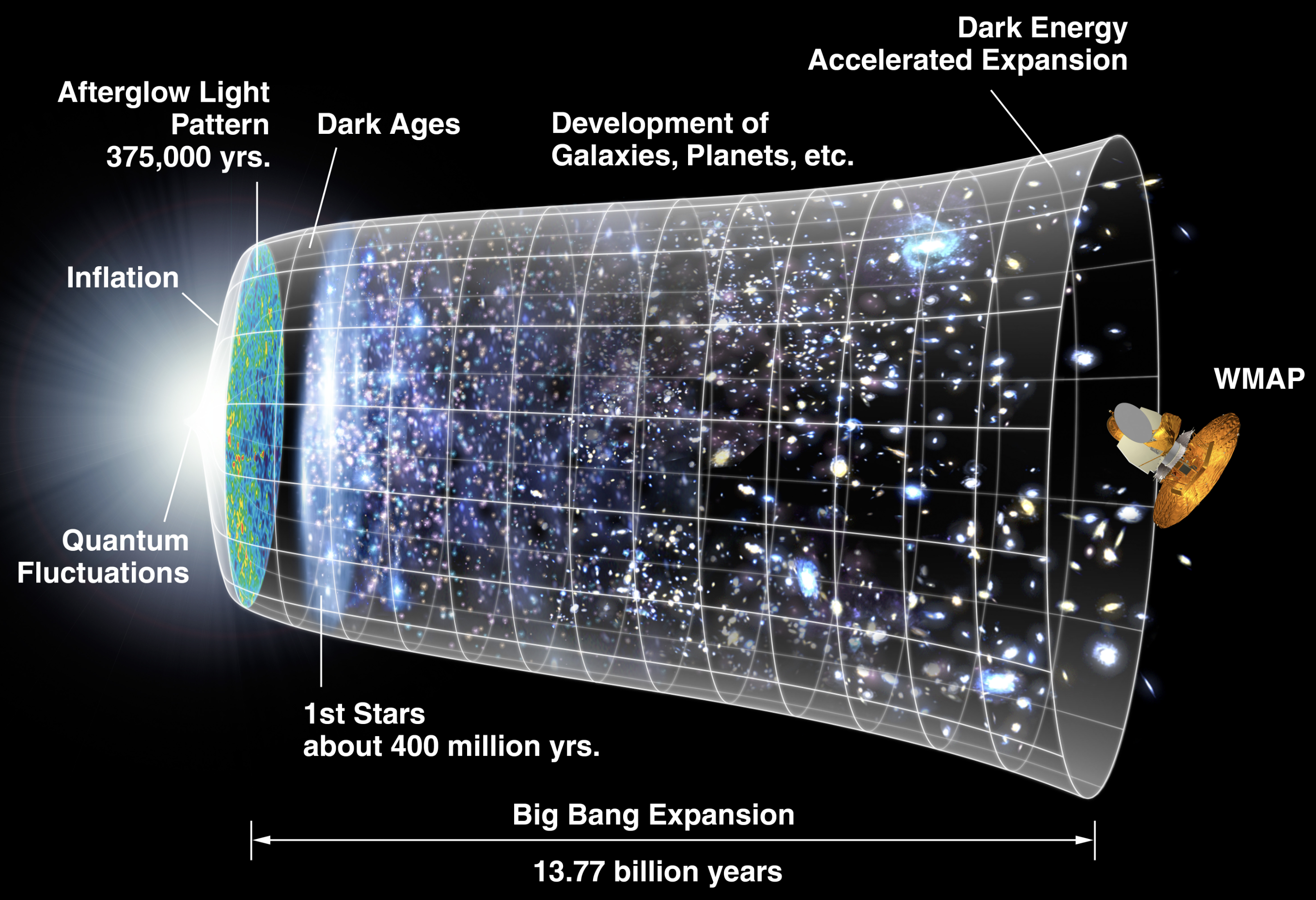
A timeline of the Universe based on the cosmic inflation theory (credit: WMAP science team/NASA)

Stephen Hawking’s final cosmology theory says the universe was created instantly (no inflation, no singularity) and it’s a hologram

There was no singularity just after the big bang (and thus, no eternal inflation) — the universe was created instantly. And there were only three dimensions. So there’s only one finite universe, not a fractal or a multiverse — and we’re living in a projected hologram. That’s what Hawking and co-author Thomas Hertog (a theoretical physicist at the Catholic University of Leuven) have concluded — contradicting Hawking’s former big-bang singularity theory (with time as a dimension).

Problem: So how does time finally emerge? “There’s a lot of work to be done,” admits Hertog. Citation (open access): Journal of High Energy Physics, May 2, 2018. Source (open access): Science, May 2, 2018


Movies capture the dynamics of an RNA molecule from the HIV-1 virus. (photo credit: Yu Xu et al.)

Molecular movies of RNA guide drug discovery — a new paradigm for drug discovery

Duke University scientists have invented a technique that combines nuclear magnetic resonance imaging and computationally generated movies to capture the rapidly changing states of an RNA molecule.

It could lead to new drug targets and allow for screening millions of potential drug candidates. So far, the technique has predicted 78 compounds (and their preferred molecular shapes) with anti-HIV activity, out of 100,000 candidate compounds. Citation: Nature Structural and Molecular Biology, May 4, 2018. Source: Duke University, May 4, 2018.


Chromium tri-iodide magnetic layers between graphene conductors. By using four layers, the storage density could be multiplied. (credit: Tiancheng Song)

Atomically thin magnetic memory

University of Washington scientists have developed the first 2D (in a flat plane) atomically thin magnetic memory — encoding information using magnets that are just a few layers of atoms in thickness — a miniaturized, high-efficiency alternative to current disk-drive materials.

In an experiment, the researchers sandwiched two atomic layers of chromium tri-iodide (CrI3) — acting as memory bits — between graphene contacts and measured the on/off electron flow through the atomic layers.

The U.S. Dept. of Energy-funded research could dramatically increase future data-storage density while reducing energy consumption by orders of magnitude. Citation: Science, May 3, 2018. Source: University of Washington, May 3, 2018.


Definitions of artificial intelligence (credit: House of Lords Select Committee on Artificial Intelligence)

A Magna Carta for the AI age

A report by the House of Lords Select Committee on Artificial Intelligence in the U.K. lays out “an overall charter for AI that can frame practical interventions by governments and other public agencies.”

The key elements: Be developed for the common good. Operate on principles of intelligibility and fairness: users must be able to easily understand the terms under which their personal data will be used. Respect rights to privacy. Be grounded in far-reaching changes to education. Teaching needs reform to utilize digital resources, and students must learn not only digital skills but also how to develop a critical perspective online. Never be given the autonomous power to hurt, destroy or deceive human beings.

Source: The Washington Post, May 2, 2018.


(credit: CB Insights)

The future of information warfare

Memes and social networks have become weaponized, but many governments seem ill-equipped to understand the new reality of information warfare.

The weapons include: Computational propaganda: digitizing the manipulation of public opinion; advanced digital deception technologies; malicious AI impersonating and manipulating people; and AI-generated fake video and audio. Counter-weapons include: Spotting AI-generated people; uncovering hidden metadata to authenticate images and videos; blockchain for tracing digital content back to the source; and detecting image and video manipulation at scale.

Source (open-access): CB Insights Research Brief, May 3, 2018.

round-up | Three radical new user interfaces

Holodeck-style holograms could revolutionize videoconferencing

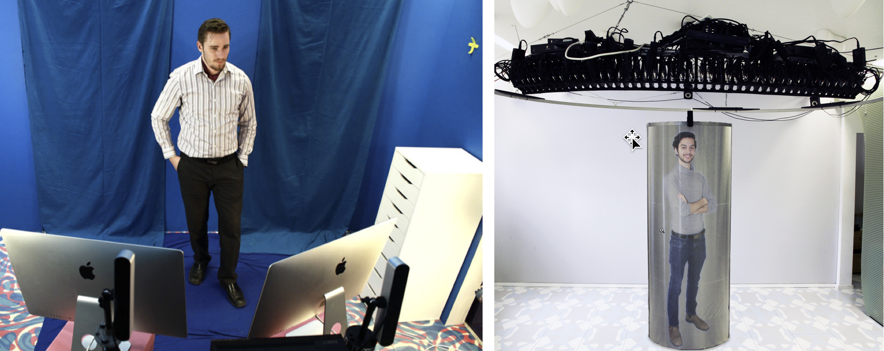
A “truly holographic” videoconferencing system has been developed by researchers at Queen’s University in Kingston Montreal. With TeleHuman 2, objects appear as stereoscopic images, as if inside a pod (not a two-dimensional video projected on a flat piece of glass). Multiple users can walk around and view the objects from all sides simultaneously — as in Star Trek’s Holodeck.

Teleporting for distance meetings. TeleHuman 2 “teleports” people live — allowing for meetings at a distance. No headset or 3D glasses required.

The researchers presented the system in an open-access paper at CHI 2018, the ACM CHI Conference on Human Factors in Computing Systems in Montreal on April 25.

(Left) Remote capture room with stereo 2K cameras, multiple surround microphones, and displays. (Right) Telehuman 2 display and projector (credit: Human Media Lab)


Interactive smart wall acts as giant touch screen, senses electromagnetic activity in room

Researchers at Carnegie Mellon University and Disney Research have devised a system called Wall++ for creating interactive “smart walls” that sense human touch, gestures, and signals from appliances.

By using masking tape and nickel-based conductive paint, a user would create a pattern of capacitive-sensing electrodes on the wall of a room (or a building) and then paint it over. The electrodes would be connected to sensors.

Wall ++ (credit: Carnegie Mellon University)

Acting as a sort of huge tablet, touch-tracking or motion-sensing uses could include dimming or turning lights on/off, controlling speaker volume, acting as smart thermostats, playing full-body video games, or creating a huge digital white board, for example.

A passive electromagnetic sensing mode could also allow for detecting devices that are on or off (by noise signature). And a small, signal-emitting wristband could enable user localization and identification for collaborative gaming or teaching, for example.

The researchers also presented an open-access paper at CHI 2018.


A smart-watch screen on your skin

LumiWatch, another interactive interface out of Carnegie Mellon, projects a smart-watch touch screen onto your skin. It solves the tiny-interface bottleneck with smart watches — providing more than five times the interactive surface area for common touchscreen operations, such as tapping and swiping. It was also presented in an open-access paper at CHI 2018.

A future ultraminiature computer the size of a pinhead?

Thin-film MRAM surface structure comprising one-monolayer iron (Fe) deposited on a boron, gallium, aluminum, or indium nitride substrate. (credit: Jie-Xiang Yu and Jiadong Zang/Science Advances)

University of New Hampshire researchers have discovered a combination of materials that they say would allow for smaller, safer magnetic random access memory (MRAM) storage — ultimately leading to ultraminiature computers.

Unlike conventional RAM (read-only memory) SRAM and DRAM chip technologies, with MRAM, data is stored by magnetic storage elements, instead of energy-expending electric charge or current flows. MRAM is also nonvolatile memory (the data is preserved when the power if turned off). The elements are formed from two ferromagnetic plates, each of which can hold a magnetization, separated by a thin insulating layer.

In their study, published March 30, 2018 in the open-access journal Science Advances, the researchers describe a new design* comprising ultrathin films, known as Fe (iron) monolayers, grown on a substrate made up of non-magnetic substances —  boron, gallium, aluminum, or indium nitride.

Ultrahigh storage density

The new design has an estimated 10-year data retention at room temperature. It can “ultimately lead to nanomagnetism and promote revolutionary ultrahigh storage density in the future,” said Jiadong Zang, an assistant professor of physics and senior author. “It opens the door to possibilities for much smaller computers for everything from basic data storage to traveling on space missions. Imagine launching a rocket with a computer the size of a pin head — it not only saves space but also a lot of fuel.”

MRAM is already challenging flash memory in a number of applications where persistent or nonvolatile memory (such as flash) is currently being used, and it’s also taking on RAM chips “in applications such as AI, IoT, 5G, and data centers,” according to a recent article in Electronic Design.**

* A provisional patent pending has been filed by UNHInnovation. This work was supported by the U.S. Department of Energy, Office of Science, Basic Energy Sciences.

** More broadly, MRAM applications are in consumer electronics, robotics, automotive , enterprise storage, and aerospace & defense, according to a market analysis and 2018–2023 forecast by Market Desk.


Abstract of Giant perpendicular magnetic anisotropy in Fe/III-V nitride thin films

Large perpendicular magnetic anisotropy (PMA) in transition metal thin films provides a pathway for enabling the intriguing physics of nanomagnetism and developing broad spintronics applications. After decades of searches for promising materials, the energy scale of PMA of transition metal thin films, unfortunately, remains only about 1 meV. This limitation has become a major bottleneck in the development of ultradense storage and memory devices. We discovered unprecedented PMA in Fe thin-film growth on the Embedded Image N-terminated surface of III-V nitrides from first-principles calculations. PMA ranges from 24.1 meV/u.c. in Fe/BN to 53.7 meV/u.c. in Fe/InN. Symmetry-protected degeneracy between x2y2 and xy orbitals and its lift by the spin-orbit coupling play a dominant role. As a consequence, PMA in Fe/III-V nitride thin films is dominated by first-order perturbation of the spin-orbit coupling, instead of second-order in conventional transition metal/oxide thin films. This game-changing scenario would also open a new field of magnetism on transition metal/nitride interfaces.
 

Intelligence-augmentation device lets users ‘speak silently’ with a computer by just thinking

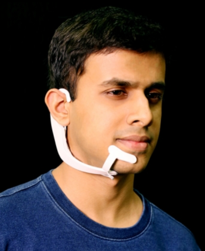
MIT Media Lab researcher Arnav Kapur demonstrates the AlterEgo device. It picks up neuromuscular facial signals generated by his thoughts; a bone-conduction headphone lets him privately hear responses from his personal devices. (credit: Lorrie Lejeune/MIT)

MIT researchers have invented a system that allows someone to communicate silently and privately with a computer or the internet by simply thinking — without requiring any facial muscle movement.

The AlterEgo system consists of a wearable device with electrodes that pick up otherwise undetectable neuromuscular subvocalizations — saying words “in your head” in natural language. The signals are fed to a neural network that is trained to identify subvocalized words from these signals. Bone-conduction headphones also transmit vibrations through the bones of the face to the inner ear to convey information to the user — privately and without interrupting a conversation. The device connects wirelessly to any external computing device via Bluetooth.

A silent, discreet, bidirectional conversation with machines. “Our idea was: Could we have a computing platform that’s more internal, that melds human and machine in some ways and that feels like an internal extension of our own cognition?,” says Arnav Kapur, a graduate student at the MIT Media Lab who led the development of the new system. Kapur is first author on an open-access paper on the research presented in March at the IUI ’18 23rd International Conference on Intelligent User Interfaces.

In one of the researchers’ experiments, subjects used the system to silently report opponents’ moves in a chess game and silently receive recommended moves from a chess-playing computer program. In another experiment, subjects were able to undetectably answer difficult computational problems, such as the square root of large numbers or obscure facts. The researchers achieved 92% median word accuracy levels, which is expected to improve.  “I think we’ll achieve full conversation someday,” Kapur said.

Non-disruptive. “We basically can’t live without our cellphones, our digital devices,” says Pattie Maes, a professor of media arts and sciences and Kapur’s thesis advisor. “But at the moment, the use of those devices is very disruptive. If I want to look something up that’s relevant to a conversation I’m having, I have to find my phone and type in the passcode and open an app and type in some search keyword, and the whole thing requires that I completely shift attention from my environment and the people that I’m with to the phone itself.

“So, my students and I have for a very long time been experimenting with new form factors and new types of experience that enable people to still benefit from all the wonderful knowledge and services that these devices give us, but do it in a way that lets them remain in the present.”*


Even the tiniest signal to her jaw or larynx might be interpreted as a command. Keeping one hand on the sensitivity knob, she concentrated to erase mistakes the machine kept interpreting as nascent words.

            Few people used subvocals, for the same reason few ever became street jugglers. Not many could operate the delicate systems without tipping into chaos. Any normal mind kept intruding with apparent irrelevancies, many ascending to the level of muttered or almost-spoken words the outer consciousness hardly noticed, but which the device manifested visibly and in sound.
            Tunes that pop into your head… stray associations you generally ignore… memories that wink in and out… impulses to action… often rising to tickle the larynx, the tongue, stopping just short of sound…
            As she thought each of those words, lines of text appeared on the right, as if a stenographer were taking dictation from her subvocalized thoughts. Meanwhile, at the left-hand periphery, an extrapolation subroutine crafted little simulations.  A tiny man with a violin. A face that smiled and closed one eye… It was well this device only read the outermost, superficial nervous activity, associated with the speech centers.
            When invented, the sub-vocal had been hailed as a boon to pilots — until high-performance jets began plowing into the ground. We experience ten thousand impulses for every one we allow to become action. Accelerating the choice and decision process did more than speed reaction time. It also shortcut judgment.
            Even as a computer input device, it was too sensitive for most people.  Few wanted extra speed if it also meant the slightest sub-surface reaction could become embarrassingly real, in amplified speech or writing.

            If they ever really developed a true brain to computer interface, the chaos would be even worse.

— From EARTH (1989) chapter 35 by David Brin (with permission)


IoT control. In the conference paper, the researchers suggest that an “internet of things” (IoT) controller “could enable a user to control home appliances and devices (switch on/off home lighting, television control, HVAC systems etc.) through internal speech, without any observable action.” Or schedule an Uber pickup.

Peripheral devices could also be directly interfaced with the system. “For instance, lapel cameras and smart glasses could directly communicate with the device and provide contextual information to and from the device. … The device also augments how people share and converse. In a meeting, the device could be used as a back-channel to silently communicate with another person.”

Applications of the technology could also include high-noise environments, like the flight deck of an aircraft carrier, or even places with a lot of machinery, like a power plant or a printing press, suggests Thad Starner, a professor in Georgia Tech’s College of Computing. “There’s a lot of places where it’s not a noisy environment but a silent environment. A lot of time, special-ops folks have hand gestures, but you can’t always see those. Wouldn’t it be great to have silent-speech for communication between these folks? The last one is people who have disabilities where they can’t vocalize normally.”

* Or users could, conceivably, simply zone out — checking texts, email messages, and twitter (all converted to voice) during boring meetings, or even reply, using mentally selected “smart reply” type options.

Next-gen optical disc has 10TB capacity and six-century lifespan

(credit: Getty)

Scientists from RMIT University in Australia and Wuhan Institute of Technology in China have developed a radical new high-capacity optical disc called “nano-optical long-data memory” that they say can record and store 10 TB (terabytes, or trillions of bytes) of data per disc securely for more than 600 years. That’s a four-times increase of storage density and 300 times increase in data lifespan over current storage technology.

Preparing  for zettabytes of data in 2025

Forecast of exponential growth of creation of Long Data, with three-year doubling time (credit: IDC)

According to IDC’s Data Age 2025 study in 2017, the recent explosion of Big Data and global cloud storage generates 2.5 PB (1015 bytes) a day, stored in massive, power-hungry data centers that use 3 percent of the world’s electricity supply. The data centers rely on hard disks, which have limited capacity (2TB per disk) and last only two years. IDC forecasts that by 2025, the global datasphere will grow exponentially to 163 zettabytes (that’s 163 trillion gigabytes) — ten times the 16.1ZB of data generated in 2016.

Examples of massive Long Data:

  • The Square Kilometer Array (SKA) radio telescope produces 576 petabytes of raw data per hour.
  • The Brain Research through Advancing Innovative Neurotechnologies (BRAIN) Initiative to map the human brain is handling data measured in yottabytes (one trillion terabytes).
  • Studying the mutation of just one human family tree over ten generations (500 years) will require 8 terabytes of data.

IDC estimates that by 2025, nearly 20% of the data in the global datasphere will be critical to our daily lives (such as biomedical data) and nearly 10% of that will be hypercritical. “By 2025, an average connected person anywhere in the world will interact with connected devices nearly 4,800 times per day — basically one interaction every 18 seconds,” the study estimates.

Replacing hard drives with optical discs

There’s a current shift from focus on “Big Data” to “Long Data,” which enables new insights to be discovered by mining massive datasets that capture changes in the real world over decades and centuries.* The researchers say their new Long-data memory technology could offer a more cost-efficient and sustainable solution to the global data storage problem.

The new technology could radically improve the energy efficiency of data centers. It would use 1000 times less power than a hard-disk-based data center by requiring far less cooling and doing away with the energy-intensive task of data migration (backing up to a new disk) every two years. Optical discs are also inherently more secure than hard disks.

“While optical technology can expand capacity, the most advanced optical discs developed so far have only 50-year lifespans,” explained lead investigator Min Gu, a professor at RMIT and senior author of an open-access paper published in Nature Communications. “Our technique can create an optical disc with the largest capacity of any optical technology developed to date and our tests have shown it will last over half a millennium and is suitable for mass production of optical discs.”

There’s an existing Blu-ray disc technology called M-DISC, that can store data for 1,000 years, but is limited to 100 GB, compared to 6000 10 TB— 100 times more data on a disc.

“This work can be the building blocks for the future of optical long-data centers over centuries, unlocking the potential of the understanding of the long processes in astronomy, geology, biology, and history,” the researchers note in the paper. “It also opens new opportunities for high-reliability optical data memory that could survive in extreme conditions, such as high temperature and high pressure.”

How the nano-optical long-data memory technology works

The high-capacity optical data memory uses gold nanoplasmonic hybrid glass composites to encode and preserve long data over centuries. (credit: Qiming Zhang et al./Nature Communications, adapted by KurzweilAI)

The new nano-optical long-data memory technology is based on a novel gold nanoplasmonic* hybrid glass matrix, unlike the materials used in current optical discs. The technique relies on a sol-gel process, which uses chemical precursors to produce ceramics and glass with higher purity and homogeneity than conventional processes. Glass is a highly durable material that can last up to 1000 years and can be used to hold data, but has limited native storage capacity because of its inflexibility. So the team combined glass with an organic material, halving its lifespan (to 600 years) but radically increasing its capacity.

Data is further encoded by heating gold nanorods, causing them to morph, in four discrete steps, into spheres. (credit: Qiming Zhang et al./Nature Communications, adapted by KurzweilAI)

To create the nanoplasmonic hybrid glass matrix, gold nanorods were incorporated into a hybrid glass composite. The researchers chose gold because like glass, it is robust and highly durable. The system allows data to be recorded in five dimensions — three dimensions in space (data is stored in gold nanorods at multiple levels in the disc and in four different shapes), plasmonic-controlled multi-color encoding**, and light-polarization encoding.

Scientists at Monash University were also involved in the research.

* “Long Data” refers here to Big Data across millennia (both historical and future), as explained here, not to be confused with the “long data” software data type. A short history of Big Data forecasts is here.

** As explained here, here, and here.

UPDATE MAR. 27, 2018 — nano-optical long-data memory disc capacity of 600TB corrected to read 10TB.


Abstract of High-capacity optical long data memory based on enhanced Young’s modulus in nanoplasmonic hybrid glass composites

Emerging as an inevitable outcome of the big data era, long data are the massive amount of data that captures changes in the real world over a long period of time. In this context, recording and reading the data of a few terabytes in a single storage device repeatedly with a century-long unchanged baseline is in high demand. Here, we demonstrate the concept of optical long data memory with nanoplasmonic hybrid glass composites. Through the sintering-free incorporation of nanorods into the earth abundant hybrid glass composite, Young’s modulus is enhanced by one to two orders of magnitude. This discovery, enabling reshaping control of plasmonic nanoparticles of multiple-length allows for continuous multi-level recording and reading with a capacity over 10 terabytes with no appreciable change of the baseline over 600 years, which opens new opportunities for long data memory that affects the past and future.

Recording data from one million neurons in real time

(credit: Getty)

Neuroscientists at the Neuronano Research Centre at Lund University in Sweden have developed and tested an ambitious new design for processing and storing the massive amounts of data expected from future implantable brain machine interfaces (BMIs) and brain-computer interfaces (BCIs).

The system would simultaneously acquire data from more than 1 million neurons in real time. It would convert the spike data (using bit encoding) and send it via an effective communication format for processing and storage on conventional computer systems. It would also provide feedback to a subject in under 25 milliseconds — stimulating up to 100,000 neurons.

Monitoring large areas of the brain in real time. Applications of this new design include basic research, clinical diagnosis, and treatment. It would be especially useful for future implantable, bidirectional BMIs and BCIs, which are used to communicate complex data between neurons and computers. This would include monitoring large areas of the brain in paralyzed patients, revealing an imminent epileptic seizure, and providing real-time feedback control to robotic arms used by quadriplegics and others.

The system is intended for recording neural signals from implanted electrodes, such as this 32-electrode grid, used for long-term, stable neural recording and treatment of neurological disorders. (credit: Thor Balkhed)

“A considerable benefit of this architecture and data format is that it doesn’t require further translation, as the brain’s [spiking] signals are translated directly into bitcode,” making it available for computer processing and dramatically increasing the processing speed and database storage capacity.

“This means a considerable advantage in all communication between the brain and computers, not the least regarding clinical applications,” says Bengt Ljungquist, lead author of the study and doctoral student at Lund University.

Future BMI/BCI systems. Current neural-data acquisition systems are typically limited to 512 or 1024 channels and the data is not easily converted into a form that can be processed and stored on PCs and other computer systems.

“The demands on hardware and software used in the context of BMI/BCI are already high, as recent studies have used recordings of up to 1792 channels for a single subject,” the researchers note in an open-access paper published in the journal Neuroinformatics.

That’s expected to increase. In 2016, DARPA (U.S. Defense Advanced Research Project Agency) announced its Neural Engineering System Design (NESD) program*, intended “to develop an implantable neural interface able to provide unprecedented signal resolution and data-transfer bandwidth between the human brain and the digital world. …

“Neural interfaces currently approved for human use squeeze a tremendous amount of information through just 100 channels, with each channel aggregating signals from tens of thousands of neurons at a time. The result is noisy and imprecise. In contrast, the NESD program aims to develop systems that can communicate clearly and individually with any of up to one million neurons in a given region of the brain.”

System architecture overview of storage for large amounts of real time neural data, proposed by Lund University researchers. A master clock pulse (a) synchronizes n acquisition systems (b), which handles bandpass filtering, spike sorting (for spike data), and down-sampling (for narrow band data), receiving electro-physiological data from subject (e). Neuronal spike data is encoded in a data grid of neurons time bins. (c). The resulting data grid is serialized and sent over to spike data storage in HDF5 file format (d), as well as to narrow band (f) and waveform data storage (g). In this work, a and b are simulated, c and d are implemented, while f and g are suggested (not yet
implemented) components. (credit: Bengt Ljungquis et al./Neuroinformatics)

* DARPA has since announced that it has “awarded contracts to five research organizations and one company that will support the Neural Engineering System Design (NESD) program: Brown University; Columbia University; Fondation Voir et Entendre (The Seeing and Hearing Foundation); John B. Pierce Laboratory; Paradromics, Inc.; and the University of California, Berkeley. These organizations have formed teams to develop the fundamental research and component technologies required to pursue the NESD vision of a high-resolution neural interface and integrate them to create and demonstrate working systems able to support potential future therapies for sensory restoration. Four of the teams will focus on vision and two will focus on aspects of hearing and speech.”


Abstract of A Bit-Encoding Based New Data Structure for Time and Memory Efficient Handling of Spike Times in an Electrophysiological Setup.

Recent neuroscientific and technical developments of brain machine interfaces have put increasing demands on neuroinformatic databases and data handling software, especially when managing data in real time from large numbers of neurons. Extrapolating these developments we here set out to construct a scalable software architecture that would enable near-future massive parallel recording, organization and analysis of neurophysiological data on a standard computer. To this end we combined, for the first time in the present context, bit-encoding of spike data with a specific communication format for real time transfer and storage of neuronal data, synchronized by a common time base across all unit sources. We demonstrate that our architecture can simultaneously handle data from more than one million neurons and provide, in real time (< 25 ms), feedback based on analysis of previously recorded data. In addition to managing recordings from very large numbers of neurons in real time, it also has the capacity to handle the extensive periods of recording time necessary in certain scientific and clinical applications. Furthermore, the bit-encoding proposed has the additional advantage of allowing an extremely fast analysis of spatiotemporal spike patterns in a large number of neurons. Thus, we conclude that this architecture is well suited to support current and near-future Brain Machine Interface requirements.

New algorithm will allow for simulating neural connections of entire brain on future exascale supercomputers

(credit: iStock)

An international team of scientists has developed an algorithm that represents a major step toward simulating neural connections in the entire human brain.

The new algorithm, described in an open-access paper published in Frontiers in Neuroinformatics, is intended to allow simulation of the human brain’s 100 billion interconnected neurons on supercomputers. The work involves researchers at the Jülich Research Centre, Norwegian University of Life Sciences, Aachen University, RIKEN, KTH Royal Institute of Technology, and KTH Royal Institute of Technology.

An open-source neural simulation tool. The algorithm was developed using NEST* (“neural simulation tool”) — open-source simulation software in widespread use by the neuroscientific community and a core simulator of the European Human Brain Project. With NEST, the behavior of each neuron in the network is represented by a small number of mathematical equations, the researchers explain in an announcement.

Since 2014, large-scale simulations of neural networks using NEST have been running on the petascale** K supercomputer at RIKEN and JUQUEEN supercomputer at the Jülich Supercomputing Centre in Germany to simulate the connections of about one percent of the neurons in the human brain, according to Markus Diesmann, PhD, Director at the Jülich Institute of Neuroscience and Medicine. Those simulations have used a previous version of the NEST algorithm.

Why supercomputers can’t model the entire brain (yet). “Before a neuronal network simulation can take place, neurons and their connections need to be created virtually,” explains senior author Susanne Kunkel of KTH Royal Institute of Technology in Stockholm.

During the simulation, a neuron’s action potentials (short electric pulses) first need to be sent to all 100,000 or so small computers, called nodes, each equipped with a number of processors doing the actual calculations. Each node then checks which of all these pulses are relevant for the virtual neurons that exist on this node.

That process requires one bit of information per processor for every neuron in the whole network. For a network of one billion neurons, a large part of the memory in each node is consumed by this single bit of information per neuron. Of course, the amount of computer memory required per processor for these extra bits per neuron increases with the size of the neuronal network. To go beyond the 1 percent and simulate the entire human brain would require the memory available to each processor to be 100 times larger than in today’s supercomputers.

In future exascale** computers, such as the post-K computer planned in Kobe and JUWELS at Jülich*** in Germany, the number of processors per compute node will increase, but the memory per processor and the number of compute nodes will stay the same.

Achieving whole-brain simulation on future exascale supercomputers. That’s where the next-generation NEST algorithm comes in. At the beginning of the simulation, the new NEST algorithm will allow the nodes to exchange information about what data on neuronal activity needs to sent and to where. Once this knowledge is available, the exchange of data between nodes can be organized such that a given node only receives the information it actually requires. That will eliminate the need for the additional bit for each neuron in the network.

Brain-simulation software, running on a current petascale supercomputer, can only represent about 1 percent of neuron connections in the cortex of a human brain (dark red area of brain on left). Only about 10 percent of neuron connections (center) would be possible on the next generation of exascale supercomputers, which will exceed the performance of today’s high-end supercomputers by 10- to 100-fold. However, a new algorithm could allow for 100 percent (whole-brain-scale simulation) on exascale supercomputers, using the same amount of computer memory as current supercomputers. (credit: Forschungszentrum Jülich, adapted by KurzweilAI)

With memory consumption under control, simulation speed will then become the main focus. For example, a large simulation of 0.52 billion neurons connected by 5.8 trillion synapses running on the supercomputer JUQUEEN in Jülich previously required 28.5 minutes to compute one second of biological time. With the improved algorithm, the time will be reduced to just 5.2 minutes, the researchers calculate.

“The combination of exascale hardware and [forthcoming NEST] software brings investigations of fundamental aspects of brain function, like plasticity and learning, unfolding over minutes of biological time, within our reach,” says Diesmann.

The new algorithm will also make simulations faster on presently available petascale supercomputers, the researchers found.

NEST simulation software update. In one of the next releases of the simulation software by the Neural Simulation Technology Initiative, the researchers will make the new open-source code freely available to the community.

For the first time, researchers will have the computer power available to simulate neuronal networks on the scale of the entire human brain.

Kenji Doya of Okinawa Institute of Science and Technology (OIST) may be among the first to try it. “We have been using NEST for simulating the complex dynamics of the basal ganglia circuits in health and Parkinson’s disease on the K computer. We are excited to hear the news about the new generation of NEST, which will allow us to run whole-brain-scale simulations on the post-K computer to clarify the neural mechanisms of motor control and mental functions,” he says .

* NEST is a simulator for spiking neural network models that focuses on the dynamics, size and structure of neural systems, rather than on the exact morphology of individual neurons. NEST is ideal for networks of spiking neurons of any size, such as models of information processing, e.g., in the visual or auditory cortex of mammals, models of network activity dynamics, e.g., laminar cortical networks or balanced random networks, and models of learning and plasticity.

** Petascale supercomputers operate at petaflop/s (quadrillions or 1015 floating point operations per second). Future exascale supercomputers will operate at exaflop/s (1018 flop/s). The fastest supercomputer at this time is the Sunway TaihuLight at the National Supercomputing Center in Wuxi, China, operating at 93 petaflops/sec.

*** At Jülich, the work is supported by the Simulation Laboratory Neuroscience, a facility of the Bernstein Network Computational Neuroscience at Jülich Supercomputing Centre. Partial funding comes from the European Union Seventh Framework Programme (Human Brain Project, HBP) and the European Union’s Horizon 2020 research and innovation programme, and the Exploratory Challenge on Post-K Computer (Understanding the neural mechanisms of thoughts and its applications to AI) of the Ministry of Education, Culture, Sports, Science and Technology (MEXT) Japan. With their joint project between Japan and Europe, the researchers hope to contribute to the formation of an International Brain Initiative (IBI).

BernsteinNetwork | NEST — A brain simulator


Abstract of Extremely Scalable Spiking Neuronal Network Simulation Code: From Laptops to Exascale Computers

State-of-the-art software tools for neuronal network simulations scale to the largest computing systems available today and enable investigations of large-scale networks of up to 10 % of the human cortex at a resolution of individual neurons and synapses. Due to an upper limit on the number of incoming connections of a single neuron, network connectivity becomes extremely sparse at this scale. To manage computational costs, simulation software ultimately targeting the brain scale needs to fully exploit this sparsity. Here we present a two-tier connection infrastructure and a framework for directed communication among compute nodes accounting for the sparsity of brain-scale networks. We demonstrate the feasibility of this approach by implementing the technology in the NEST simulation code and we investigate its performance in different scaling scenarios of typical network simulations. Our results show that the new data structures and communication scheme prepare the simulation kernel for post-petascale high-performance computing facilities without sacrificing performance in smaller systems.