Superconducting ‘synapse’ could enable powerful future neuromorphic supercomputers

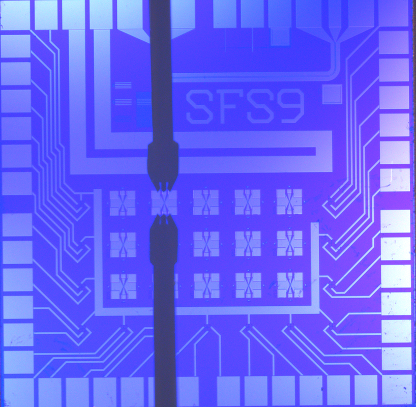
NIST’s artificial synapse, designed for neuromorphic computing, mimics the operation of switch between two neurons. One artificial synapse is located at the center of each X. This chip is 1 square centimeter in size. (The thick black vertical lines are electrical probes used for testing.) (credit: NIST)

A superconducting “synapse” that “learns” like a biological system, operating like the human brain, has been built by researchers at the National Institute of Standards and Technology (NIST).

The NIST switch, described in an open-access paper in Science Advances, provides a missing link for neuromorphic (brain-like) computers, according to the researchers. Such “non-von Neumann architecture” future computers could significantly speed up analysis and decision-making for applications such as self-driving cars and cancer diagnosis.

The research is supported by the Intelligence Advanced Research Projects Activity (IARPA) Cryogenic Computing Complexity Program, which was launched in 2014 with the goal of paving the way to “a new generation of superconducting supercomputer development beyond the exascale.”*

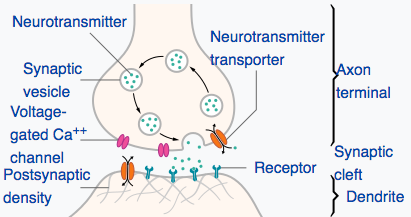
A synapse is a connection or switch between two neurons, controlling transmission of signals. (credit: NIST)

NIST’s artificial synapse is a metallic cylinder 10 micrometers in diameter — about 10 times larger than a biological synapse. It simulates a real synapse by processing incoming electrical spikes (pulsed current from a neuron) and customizing spiking output signals. The more firing between cells (or processors), the stronger the connection. That process enables both biological and artificial synapses to maintain old circuits and create new ones.

Dramatically faster, lower-energy-required, compared to human synapses

But the NIST synapse has two unique features that the researchers say are superior to human synapses and to other artificial synapses:

  • Operating at 100 GHz, it can fire at a rate that is much faster than the human brain — 1 billion times per second, compared to a brain cell’s rate of about 50 times per second.
  • It uses only about one ten-thousandth as much energy as a human synapse. The spiking energy is less than 1 attojoule** — roughly equivalent to the miniscule chemical energy bonding two atoms in a molecule — compared to the roughly 10 femtojoules (10,000 attojoules) per synaptic event in the human brain. Current neuromorphic platforms are orders of magnitude less efficient than the human brain. “We don’t know of any other artificial synapse that uses less energy,” NIST physicist Mike Schneider said.

Superconducting devices mimicking brain cells and transmission lines have been developed, but until now, efficient synapses — a crucial piece — have been missing. The new Josephson junction-based artificial synapse would be used in neuromorphic computers made of superconducting components (which can transmit electricity without resistance), so they would be more efficient than designs based on semiconductors or software. Data would be transmitted, processed, and stored in units of magnetic flux.

The brain is especially powerful for tasks like image recognition because it processes data both in sequence and simultaneously and it stores memories in synapses all over the system. A conventional computer processes data only in sequence and stores memory in a separate unit.

The new NIST artificial synapses combine small size, superfast spiking signals, and low energy needs, and could be stacked into dense 3D circuits for creating large systems. They could provide a unique route to a far more complex and energy-efficient neuromorphic system than has been demonstrated with other technologies, according to the researchers.

Nature News does raise some concerns about the research, quoting neuromorphic-technology experts: “Millions of synapses would be necessary before a system based on the technology could be used for complex computing; it remains to be seen whether it will be possible to scale it to this level. … The synapses can only operate at temperatures close to absolute zero, and need to be cooled with liquid helium. That this might make the chips impractical for use in small devices, although a large data centre might be able to maintain them. … We don’t yet understand enough about the key properties of the [biological] synapse to know how to use them effectively.”


Inside a superconducting synapse 

The NIST synapse is a customized Josephson junction***, long used in NIST voltage standards. These junctions are a sandwich of superconducting materials with an insulator as a filling. When an electrical current through the junction exceeds a level called the critical current, voltage spikes are produced.

Illustration showing the basic operation of NIST’s artificial synapse, based on a Josephson junction. Very weak electrical current pulses are used to control the number of nanoclusters (green) pointing in the same direction. Shown here: a “magnetically disordered state” (left) vs. “magnetically ordered state” (right). (credit: NIST)

Each artificial synapse uses standard niobium electrodes but has a unique filling made of nanoscale clusters (“nanoclusters”) of manganese in a silicon matrix. The nanoclusters — about 20,000 per square micrometer — act like tiny bar magnets with “spins” that can be oriented either randomly or in a coordinated manner. The number of nanoclusters pointing in the same direction can be controlled, which affects the superconducting properties of the junction.

Diagram of circuit used in the simulation. The blue and red areas represent pre- and post-synapse neurons, respectively. The X symbol represents the Josephson junction. (credit: Michael L. Schneider et al./Science Advances)

The synapse rests in a superconducting state, except when it’s activated by incoming current and starts producing voltage spikes. Researchers apply current pulses in a magnetic field to boost the magnetic ordering — that is, the number of nanoclusters pointing in the same direction.

This magnetic effect progressively reduces the critical current level, making it easier to create a normal conductor and produce voltage spikes. The critical current is the lowest when all the nanoclusters are aligned. The process is also reversible: Pulses are applied without a magnetic field to reduce the magnetic ordering and raise the critical current. This design, in which different inputs alter the spin alignment and resulting output signals, is similar to how the brain operates.

Synapse behavior can also be tuned by changing how the device is made and its operating temperature. By making the nanoclusters smaller, researchers can reduce the pulse energy needed to raise or lower the magnetic order of the device. Raising the operating temperature slightly from minus 271.15 degrees C (minus 456.07 degrees F) to minus 269.15 degrees C (minus 452.47 degrees F), for example, results in more and higher voltage spikes.


* Future exascale supercomputers would run at 1018 exaflops (“flops” = floating point operations per second) or more. The current fastest supercomputer — the Sunway TaihuLight — operates at about 0.1 exaflops; zettascale computers, the next step beyond exascale, would run 10,000 times faster than that.

** An attojoule is 10-18 joule, a unit of energy, and is one-thousandth of a femtojoule.

*** The Josephson effect is the phenomenon of supercurrent — i.e., a current that flows indefinitely long without any voltage applied — across a device known as a Josephson junction, which consists of two superconductors coupled by a weak link. — Wikipedia


Abstract of Ultralow power artificial synapses using nanotextured magnetic Josephson junctions

Neuromorphic computing promises to markedly improve the efficiency of certain computational tasks, such as perception and decision-making. Although software and specialized hardware implementations of neural networks have made tremendous accomplishments, both implementations are still many orders of magnitude less energy efficient than the human brain. We demonstrate a new form of artificial synapse based on dynamically reconfigurable superconducting Josephson junctions with magnetic nanoclusters in the barrier. The spiking energy per pulse varies with the magnetic configuration, but in our demonstration devices, the spiking energy is always less than 1 aJ. This compares very favorably with the roughly 10 fJ per synaptic event in the human brain. Each artificial synapse is composed of a Si barrier containing Mn nanoclusters with superconducting Nb electrodes. The critical current of each synapse junction, which is analogous to the synaptic weight, can be tuned using input voltage spikes that change the spin alignment of Mn nanoclusters. We demonstrate synaptic weight training with electrical pulses as small as 3 aJ. Further, the Josephson plasma frequencies of the devices, which determine the dynamical time scales, all exceed 100 GHz. These new artificial synapses provide a significant step toward a neuromorphic platform that is faster, more energy-efficient, and thus can attain far greater complexity than has been demonstrated with other technologies.

Penn researchers create first optical transistor comparable to an electronic transistor

By precisely controlling the mixing of optical signals, Ritesh Agarwal’s research team says they have taken an important step toward photonic (optical) computing. (credit: Sajal Dhara)

In an open-access paper published in Nature Communications, Ritesh Agarwal, a professor the University of Pennsylvania School of Engineering and Applied Science, and his colleagues say that they have made significant progress in photonic (optical) computing by creating a prototype of a working optical transistor with properties similar to those of a conventional electronic transistor.*

Optical transistors, using photons instead of electrons, promise to one day be more powerful than the electronic transistors currently used in computers.

Agarwal’s research on photonic computing has been focused on finding the right combination and physical configuration of nonlinear materials that can amplify and mix light waves in ways that are analogous to electronic transistors. “One of the hurdles in doing this with light is that materials that are able to mix optical signals also tend to have very strong background signals as well. That background signal would drastically reduce the contrast and on/off ratios leading to errors in the output,” Agarwal explained.

How the new optical transistor works

Schematic of a cadmium sulfide nanobelt device with source (S) and drain (D) electrodes. The fundamental wave at the frequency of ω, which is normally incident upon the belt, excites the second-harmonic (twice the frequency) wave at 2ω, which is back-scattered. (credit: Ming-Liang Ren et al./Nature Communications)

To address this issue, Agarwal’s research group started by creating a system with no disruptive optical background signal. To do that, they used a “nanobelt”* made out of cadmium sulfide. Then, by applying an electrical field across the nanobelt, the researchers were able to introduce optical nonlinearities (similar to the nonlinearities in electronic transistors), which enabled a signal mixing output that was otherwise zero.

“Our system turns on from zero to extremely large values,” Agarwal said.** “For the first time, we have an optical device with output that truly resembles an electronic transistor.”

The next steps toward a fully functioning photonic computer will involve integrating optical circuits with optical interconnects, modulators, and detectors to achieve actual on-chip integrated photonic computation.

The research was supported by the US Army Research Office and the National Science Foundation.

* “Made of semiconducting metal oxides, nanobelts are extremely thin and flat structures. They are chemically pure, structurally uniform, largely defect-free, with clean surfaces that do not require protection against oxidation. Each is made up of a single crystal with specific surface planes and shape.” — Reade International Corp.

** That is, the system was capable of precisely controlling the mixing of optical signals via controlled electric fields, with outputs with near-perfect contrast and extremely large on/off ratios. “Our study demonstrates a new way to dynamically control nonlinear optical signals in nanoscale materials with ultrahigh signal contrast and signal saturation, which can enable the development of nonlinear optical transistors and modulators for on-chip photonic devices with high-performance metrics and small-form factors, which can be further enhanced by integrating with nanoscale optical cavities,” the researchers note in the paper.


Abstract of Strong modulation of second-harmonic generation with very large contrast in semiconducting CdS via high-field domain

Dynamic control of nonlinear signals is critical for a wide variety of optoelectronic applications, such as signal processing for optical computing. However, controlling nonlinear optical signals with large modulation strengths and near-perfect contrast remains a challenging problem due to intrinsic second-order nonlinear coefficients via bulk or surface contributions. Here, via electrical control, we turn on and tune second-order nonlinear coefficients in semiconducting CdS nanobelts from zero to up to 151 pm V−1, a value higher than other intrinsic nonlinear coefficients in CdS. We also observe ultrahigh ON/OFF ratio of >104 and modulation strengths ~200% V−1 of the nonlinear signal. The unusual nonlinear behavior, including super-quadratic voltage and power dependence, is ascribed to the high-field domain, which can be further controlled by near-infrared optical excitation and electrical gating. The ability to electrically control nonlinear optical signals in nanostructures can enable optoelectronic devices such as optical transistors and modulators for on-chip integrated photonics.

Ultra-thin ‘atomistor’ synapse-like memory storage device paves way for faster, smaller, smarter computer chips

Illustration of single-atom-layer “atomristors” — the thinnest-ever memory-storage device (credit: Cockrell School of Engineering, The University of Texas at Austin)

A team of electrical engineers at The University of Texas at Austin and scientists at Peking University has developed a one-atom-thick 2D “atomristor” memory storage device that may lead to faster, smaller, smarter computer chips.

The atomristor (atomic memristor) improves upon memristor (memory resistor) memory storage technology by using atomically thin nanomaterials (atomic sheets). (Combining memory and logic functions, similar to the synapses of biological brains, memristors “remember” their previous state after being turned off.)

Schematic of atomristor memory sandwich based on molybdenum sulfide (MoS2) in a form of a single-layer atomic sheet grown on gold foil. (Blue: Mo; yellow: S) (credit: Ruijing Ge et al./Nano Letters)

Memory storage and transistors have, to date, been separate components on a microchip. Atomristors combine both functions on a single, more-efficient device. They use metallic atomic sheets (such as graphene or gold) as electrodes and semiconducting atomic sheets (such as molybdenum sulfide) as the active layer. The entire memory cell is a two-layer sandwich only ~1.5 nanometers thick.

“The sheer density of memory storage that can be made possible by layering these synthetic atomic sheets onto each other, coupled with integrated transistor design, means we can potentially make computers that learn and remember the same way our brains do,” said Deji Akinwande, associate professor in the Cockrell School of Engineering’s Department of Electrical and Computer Engineering.

“This discovery has real commercialization value, as it won’t disrupt existing technologies,” Akinwande said. “Rather, it has been designed to complement and integrate with the silicon chips already in use in modern tech devices.”

The research is described in an open-access paper in the January American Chemical Society journal Nano Letters.

Longer battery life in cell phones

For nonvolatile operation (preserving data after power is turned off), the new design also “offers a substantial advantage over conventional flash memory, which occupies far larger space. In addition, the thinness allows for faster and more efficient electric current flow,” the researchers note in the paper.

The research team also discovered another unique application for the atomristor technology: Atomristors are the smallest radio-frequency (RF) memory switches to be demonstrated, with no DC battery consumption, which could ultimately lead to longer battery life for cell phones and other battery-powered devices.*

Funding for the UT Austin team’s work was provided by the National Science Foundation and the Presidential Early Career Award for Scientists and Engineers, awarded to Akinwande in 2015.

* “Contemporary switches are realized with transistor or microelectromechanical devices, both of which are volatile, with the latter also requiring large switching voltages [which are not ideal] for mobile technologies,” the researchers note in the paper. Atomristors instead allow for nonvolatile low-power radio-frequency (RF) switches with “low voltage operation, small form-factor, fast switching speed, and low-temperature integration compatible with silicon or flexible substrates.”


Abstract of Atomristor: Nonvolatile Resistance Switching in Atomic Sheets of Transition Metal Dichalcogenides

Recently, two-dimensional (2D) atomic sheets have inspired new ideas in nanoscience including topologically protected charge transport,1,2 spatially separated excitons,3 and strongly anisotropic heat transport.4 Here, we report the intriguing observation of stable nonvolatile resistance switching (NVRS) in single-layer atomic sheets sandwiched between metal electrodes. NVRS is observed in the prototypical semiconducting (MX2, M = Mo, W; and X = S, Se) transitional metal dichalcogenides (TMDs),5 which alludes to the universality of this phenomenon in TMD monolayers and offers forming-free switching. This observation of NVRS phenomenon, widely attributed to ionic diffusion, filament, and interfacial redox in bulk oxides and electrolytes,6−9 inspires new studies on defects, ion transport, and energetics at the sharp interfaces between atomically thin sheets and conducting electrodes. Our findings overturn the contemporary thinking that nonvolatile switching is not scalable to subnanometre owing to leakage currents.10 Emerging device concepts in nonvolatile flexible memory fabrics, and brain-inspired (neuromorphic) computing could benefit substantially from the wide 2D materials design space. A new major application, zero-static power radio frequency (RF) switching, is demonstrated with a monolayer switch operating to 50 GHz.

An artificial synapse for future miniaturized portable ‘brain-on-a-chip’ devices

Biological synapse structure (credit: Thomas Splettstoesser/CC)

MIT engineers have designed a new artificial synapse made from silicon germanium that can precisely control the strength of an electric current flowing across it.

In simulations, the researchers found that the chip and its synapses could be used to recognize samples of handwriting with 95 percent accuracy. The engineers say the new design, published today (Jan. 22) in the journal Nature Materials, is a major step toward building portable, low-power neuromorphic chips for use in pattern recognition and other machine-learning tasks.

Controlling the flow of ions: the challenge

Researchers in the emerging field of “neuromorphic computing” have attempted to design computer chips that work like the human brain. The idea is to apply a voltage across layers that would cause ions (electrically charged atoms) to move in a switching medium (synapse-like space) to create conductive filaments in a manner that’s similar to how the “weight” (connection strength) of a synapse changes.

There are more than 100 trillion synapses (in a typical human brain) that mediate neuron signaling in the brain, strengthening some neural connections while pruning (weakening) others — a process that enables the brain to recognize patterns, remember facts, and carry out other learning tasks, all at lightning speeds.

Instead of carrying out computations based on binary, on/off signaling, like current digital chips, the elements of a “brain on a chip” would work in an analog fashion, exchanging a gradient of signals, or “weights” — much like neurons that activate in various ways (depending on the type and number of ions that flow across a synapse).

But it’s been difficult to control the flow of ions in existing synapse designs. These have multiple paths that make it difficult to predict where ions will make it through, according to research team leader Jeehwan Kim, PhD, an assistant professor in the departments of Mechanical Engineering and Materials Science and Engineering, a principal investigator in MIT’s Research Laboratory of Electronics and Microsystems Technology Laboratories.

“Once you apply some voltage to represent some data with your artificial neuron, you have to erase and be able to write it again in the exact same way,” Kim says. “But in an amorphous solid, when you write again, the ions go in different directions because there are lots of defects. This stream is changing, and it’s hard to control. That’s the biggest problem — nonuniformity of the artificial synapse.”

Epitaxial random access memory (epiRAM)

(Left) Cross-sectional transmission electron microscope image of 60 nm silicon-germanium (SiGe) crystal grown on a silicon substrate (diagonal white lines represent candidate dislocations). Scale bar: 25 nm. (Right) Cross-sectional scanning electron microscope image of an epiRAM device with titanium (Ti)–gold (Au) and silver (Ag)–palladium (Pd) layers. Scale bar: 100 nm. (credit: Shinhyun Choi et al./Nature Materials)

So instead of using amorphous materials as an artificial synapse, Kim and his colleagues created an new “epitaxial random access memory” (epiRAM) design.

They started with a wafer of silicon. They then grew a similar pattern of silicon germanium — a material used commonly in transistors — on top of the silicon wafer. Silicon germanium’s lattice is slightly larger than that of silicon, and Kim found that together, the two perfectly mismatched materials could form a funnel-like dislocation, creating a single path through which ions can predictably flow.*

This is the most uniform device we could achieve, which is the key to demonstrating artificial neural networks,” Kim says.

Testing the ability to recognize samples of handwriting

As a test, Kim and his team explored how the epiRAM device would perform if it were to carry out an actual learning task: recognizing samples of handwriting — which researchers consider to be a practical test for neuromorphic chips. Such chips would consist of artificial “neurons” connected to other “neurons” via filament-based artificial “synapses.”

Image-recognition simulation. (Left) A 3-layer multilayer-perception neural network with black and white input signal for each layer in algorithm level. The inner product (summation) of input neuron signal vector and first synapse array vector is transferred after activation and binarization as input vectors of second synapse arrays. (Right) Circuit block diagram of hardware implementation showing a synapse layer composed of epiRAM crossbar arrays and the peripheral circuit. (credit: Shinhyun Choi et al./Nature Materials)

They ran a computer simulation of an artificial neural network consisting of three sheets of neural layers connected via two layers of artificial synapses, based on measurements from their actual neuromorphic chip. They fed into their simulation tens of thousands of samples from the MNIST handwritten recognition dataset**, commonly used by neuromorphic designers.

They found that their neural network device recognized handwritten samples 95.1 percent of the time — close to the 97 percent accuracy of existing software algorithms running on large computers.

A chip to replace a supercomputer

The team is now in the process of fabricating a real working neuromorphic chip that can carry out handwriting-recognition tasks. Looking beyond handwriting, Kim says the team’s artificial synapse design will enable much smaller, portable neural network devices that can perform complex computations that are currently only possible with large supercomputers.

“Ultimately, we want a chip as big as a fingernail to replace one big supercomputer,” Kim says. “This opens a stepping stone to produce real artificial intelligence hardware.”

This research was supported in part by the National Science Foundation. Co-authors included researchers at Arizona State University.

* They applied voltage to each synapse and found that all synapses exhibited about the same current, or flow of ions, with about a 4 percent variation between synapses — a much more uniform performance compared with synapses made from amorphous material. They also tested a single synapse over multiple trials, applying the same voltage over 700 cycles, and found the synapse exhibited the same current, with just 1 percent variation from cycle to cycle.

** The MNIST (Modified National Institute of Standards and Technology database) is a large database of handwritten digits that is commonly used for training various image processing systems and for training and testing in the field of machine learning. It contains 60,000 training images and 10,000 testing images. 


Abstract of SiGe epitaxial memory for neuromorphic computing with reproducible high performance based on engineered dislocations

Although several types of architecture combining memory cells and transistors have been used to demonstrate artificial synaptic arrays, they usually present limited scalability and high power consumption. Transistor-free analog switching devices may overcome these limitations, yet the typical switching process they rely on—formation of filaments in an amorphous medium—is not easily controlled and hence hampers the spatial and temporal reproducibility of the performance. Here, we demonstrate analog resistive switching devices that possess desired characteristics for neuromorphic computing networks with minimal performance variations using a single-crystalline SiGe layer epitaxially grown on Si as a switching medium. Such epitaxial random access memories utilize threading dislocations in SiGe to confine metal filaments in a defined, one-dimensional channel. This confinement results in drastically enhanced switching uniformity and long retention/high endurance with a high analog on/off ratio. Simulations using the MNIST handwritten recognition data set prove that epitaxial random access memories can operate with an online learning accuracy of 95.1%.

Amazon’s store of the future opens

(credit: Amazon)

Amazon’s first Amazon Go store opened today in Seattle, automating most of the purchase, checkout, and payment steps associated with a retail transaction and replacing cash registers, cashiers, credit cards, self-checkout kiosks, RFID chips — and lines — with hundreds of small cameras, computer vision, deep-learning algorithms, and sensor fusion.

Just walk in (as long as you have the Amazon Go app and an Amazon.com account), scan a QR code at the turnstile, grab, and go.

Meanwhile, the shutdown of the dysfunctional U.S. government continues.* Hmm, what if we created Government Go?

If you visit the store (2131 7th Ave — 7 a.m. to 9 p.m. PT Monday to Friday), let us know about your experience and thoughts in the comments below.

* January 22 at 6:11 PM EST: House votes to end government shutdown, sending legislation to Trump — Washington Post

Remote-controlled DNA nanorobots could lead to the first nanorobotic production factory

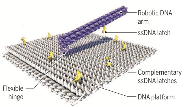
German researchers created a 55-nm-by-55-nm DNA-based molecular platform with a 25-nm-long robotic arm that can be actuated with externally applied electrical fields, under computer control. (credit: Enzo Kopperger et al./Science)

By powering a self-assembling DNA nanorobotic arm with electric fields, German scientists have achieved precise nanoscale movement that is at least five orders of magnitude (hundreds of thousands times) faster than previously reported DNA-driven robotic systems, they suggest today (Jan. 19) in the journal Science.

DNA origami has emerged as a powerful tool to build precise structures. But now, “Kopperger et al. make an impressive stride in this direction by creating a dynamic DNA origami structure that they can directly control from the macroscale with easily tunable electric fields—similar to a remote-controlled robot,” notes Björn Högberg of Karolinska Institutet in a related Perspective in Science, (p. 279).

The nanorobotic arm resembles the gearshift lever of a car. Controlled by an electric field (comparable to the car driver), short, single-stranded DNA serves as “latches” (yellow) to momentarily grab and lock the 25-nanometer-long arm into predefined “gear” positions. (credit: Enzo Kopperger et al./Science)

The new biohybrid nanorobotic systems could even act as a molecular mechanical memory (a sort of nanoscale version of the Babbage Analytical Engine), he notes. “With the capability to form long filaments with multiple DNA robot arms, the systems could also serve as a platform for new inventions in digital memory, nanoscale cargo transfer, and 3D printing of molecules.”

“The robot-arm system may be scaled up and integrated into larger hybrid systems by a combination of lithographic and self-assembly techniques,” according to the researchers. “Electrically clocked synthesis of molecules with a large number of robot arms in parallel could then be the first step toward the realization of a genuine nanorobotic production factory.”


Taking a different approach to a nanofactory, this “Productive Nanosystems: from Molecules to Superproducts” film — a collaborative project of animator and engineer John Burch and pioneer nanotechnologist K. Eric Drexler in 2005 — demonstrated key steps in a hypothetical process that converts simple molecules into a billion-CPU laptop computer. More here.


Abstract of A self-assembled nanoscale robotic arm controlled by electric fields

The use of dynamic, self-assembled DNA nanostructures in the context of nanorobotics requires fast and reliable actuation mechanisms. We therefore created a 55-nanometer–by–55-nanometer DNA-based molecular platform with an integrated robotic arm of length 25 nanometers, which can be extended to more than 400 nanometers and actuated with externally applied electrical fields. Precise, computer-controlled switching of the arm between arbitrary positions on the platform can be achieved within milliseconds, as demonstrated with single-pair Förster resonance energy transfer experiments and fluorescence microscopy. The arm can be used for electrically driven transport of molecules or nanoparticles over tens of nanometers, which is useful for the control of photonic and plasmonic processes. Application of piconewton forces by the robot arm is demonstrated in force-induced DNA duplex melting experiments.

DARPA-funded ‘unhackable’ computer could avoid future flaws like Spectre and Meltdown

(credit: University of Michigan)

A University of Michigan (U-M) team has announced plans to develop an “unhackable” computer, funded by a new $3.6 million grant from the Defense Advanced Research Projects Agency (DARPA).

The goal of the project, called MORPHEUS, is to design computers that avoid the vulnerabilities of most current microprocessors, such as the Spectre and Meltdown flaws announced  last week.*

The $50 million DARPA System Security Integrated Through Hardware and Firmware (SSITH) program aims to build security right into chips’ microarchitecture, instead of relying on software patches.*

The U-M grant is one of nine that DARPA has recently funded through SSITH.

Future-proofing

The idea is to protect against future threats that have yet to be identified. “Instead of relying on software Band-Aids to hardware-based security issues, we are aiming to remove those hardware vulnerabilities in ways that will disarm a large proportion of today’s software attacks,” said Linton Salmon, manager of DARPA’s System Security Integrated Through Hardware and Firmware program.

Under MORPHEUS, the location of passwords would constantly change, for example. And even if an attacker were quick enough to locate the data, secondary defenses in the form of encryption and domain enforcement would throw up additional roadblocks.

More than 40 percent of the “software doors” that hackers have available to them today would be closed if researchers could eliminate seven classes of hardware weaknesses**, according to DARPA.

DARPA is aiming to render these attacks impossible within five years. “If developed, MORPHEUS could do it now,” said Todd Austin, U-M professor of computer science and engineering, who leads the project. Researchers at The University of Texas and Princeton University are also working with U-M.

* Apple released today (Jan. 8) iOS 11.2.2 and macOS 10.13.2 updates with Spectre fix for Safari and WebKit, according to MacWorld. Threatpost has an update (as of Jan. 7) on efforts by Intel and others in dealing with Meltdown and Spectre processor vulnerabilities .

** Permissions and privileges, buffer errors, resource management, information leakage, numeric errors, crypto errors, and code injection.

UPDATE 1/9/2018: BLUE-SCREEN ALERT: Read this if you have a Windows computer with an AMD processor: Microsoft announced today it has temporarily paused sending some Windows operating system updates (intended to protect against Spectre and Meltdown chipset vulnerabilities) to devices that have impacted AMD processors. “Microsoft has received reports of some AMD devices getting into an unbootable state after installation of recent Windows operating system security updates.”


Using light instead of electrons promises faster, smaller, more-efficient computers and smartphones

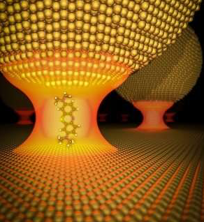
Trapped light for optical computation (credit: Imperial College London)

By forcing light to go through a smaller gap than ever before, a research team at Imperial College London has taken a step toward computers based on light instead of electrons.

Light would be preferable for computing because it can carry much-higher-density information, it’s much faster, and more efficient (generates little to no heat). But light beams don’t easily interact with one other. So information on high-speed fiber-optic cables (provided by your cable TV company, for example) currently has to be converted (via a modem or other device) into slower signals (electrons on wires or wireless signals) to allow for processing the data on devices such as computers and smartphones.

Electron-microscope image of an optical-computing nanofocusing device that is 25 nanometers wide and 2 micrometers long, using grating couplers (vertical lines) to interface with fiber-optic cables. (credit: Nielsen et al., 2017/Imperial College London)

To overcome that limitation, the researchers used metamaterials to squeeze light into a metal channel only 25 nanometers (billionths of a meter) wide, increasing its intensity and allowing photons to interact over the range of micrometers (millionths of meters) instead of centimeters.*

That means optical computation that previously required a centimeters-size device can now be realized on the micrometer (one millionth of a meter) scale, bringing optical processing into the size range of electronic transistors.

The results were published Thursday Nov. 30, 2017 in the journal Science.

* Normally, when two light beams cross each other, the individual photons do not interact or alter each other, as two electrons do when they meet. That means a long span of material is needed to gradually accumulate the effect and make it useful. Here, a “plasmonic nanofocusing” waveguide is used, strongly confining light within a nonlinear organic polymer.


Abstract of Giant nonlinear response at a plasmonic nanofocus drives efficient four-wave mixing

Efficient optical frequency mixing typically must accumulate over large interaction lengths because nonlinear responses in natural materials are inherently weak. This limits the efficiency of mixing processes owing to the requirement of phase matching. Here, we report efficient four-wave mixing (FWM) over micrometer-scale interaction lengths at telecommunications wavelengths on silicon. We used an integrated plasmonic gap waveguide that strongly confines light within a nonlinear organic polymer. The gap waveguide intensifies light by nanofocusing it to a mode cross-section of a few tens of nanometers, thus generating a nonlinear response so strong that efficient FWM accumulates over wavelength-scale distances. This technique opens up nonlinear optics to a regime of relaxed phase matching, with the possibility of compact, broadband, and efficient frequency mixing integrated with silicon photonics.

New magnetism-control method could lead to ultrafast, energy-efficient computer memory

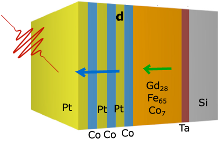
A cobalt layer on top of a gadolinium-iron alloy allows for switching memory with a single laser pulse in just 7 picoseconds. The discovery may lead to a computing processor with high-speed, non-volatile memory right on the chip. (credit: Jon Gorchon et al./Applied Physics Letters)

Researchers at UC Berkeley and UC Riverside have developed an ultrafast new method for electrically controlling magnetism in certain metals — a breakthrough that could lead to more energy-efficient computer memory and processing technologies.

“The development of a non-volatile memory that is as fast as charge-based random-access memories could dramatically improve performance and energy efficiency of computing devices,” says Berkeley electrical engineering and computer sciences (EECS) professor Jeffrey Bokor, coauthor of a paper on the research in the open-access journal Science Advances. “That motivated us to look for new ways to control magnetism in materials at much higher speeds than in today’s MRAM.”


Background: RAM vs. MRAM memory

Computers use different kinds of memory technologies to store data. Long-term memory, typically a hard disk or flash drive, needs to be dense in order to store as much data as possible but is slow. The central processing unit (CPU) — the hardware that enables computers to compute — requires fast memory to keep up with the CPU’s calculations, so the memory is only used for short-term storage of information (while operations are executed).

Random access memory (RAM) is one example of such short-term memory. Most current RAM technologies are based on charge (electron) retention, and can be written at rates of billions of bits per second (bits/nanosecond). The downside of these charge-based technologies is that they are volatile, requiring constant power or else they will lose the data.

In recent years, “spintronics” magnetic alternatives to RAM, known as Magnetic Random Access Memory (MRAM), have reached the market. The advantage of using magnets is that they retain information even when memory and CPU are powered off, allowing for energy savings. But that efficiency comes at the expense of speed, which is on the order of hundreds of picoseconds to write a single bit of information. (For comparison, silicon field-effect transistors have switching delays less than 5 picoseconds.)


The researchers found a magnetic alloy made up of gadolinium and iron that could accomplish those higher speeds — switching the direction of the magnetism with a series of electrical pulses of about 10 picoseconds (one picosecond is 1,000 times shorter than one nanosecond) — more than 10 times faster than MRAM.*

A faster version, using an energy-efficient optical pulse

In a second study, published in Applied Physics Letters, the researchers were able to further improve the performance by stacking a single-element magnetic metal such as cobalt on top of the gadolinium-iron alloy, allowing for switching with a single laser pulse in just 7 picoseconds. As a single pulse, it was also more energy-efficient. The result was a computing processor with high-speed, non-volatile memory right on the chip, functionally similar to an IBM Research “in-memory” computing architecture profiled in a recent KurzweilAI article.

“Together, these two discoveries provide a route toward ultrafast magnetic memories that enable a new generation of high-performance, low-power computing processors with high-speed, non-volatile memories right on chip,” Bokor says.

The research was supported by grants from the National Science Foundation and the U.S. Department of Energy.

* The electrical pulse temporarily increases the energy of the iron atom’s electrons, causing the magnetism in the iron and gadolinium atoms to exert torque on one another, and eventually leads to a reorientation of the metal’s magnetic poles. It’s a completely new way of using electrical currents to control magnets, according to the researchers.


Abstract of Ultrafast magnetization reversal by picosecond electrical pulses

The field of spintronics involves the study of both spin and charge transport in solid-state devices. Ultrafast magnetism involves the use of femtosecond laser pulses to manipulate magnetic order on subpicosecond time scales. We unite these phenomena by using picosecond charge current pulses to rapidly excite conduction electrons in magnetic metals. We observe deterministic, repeatable ultrafast reversal of the magnetization of a GdFeCo thin film with a single sub–10-ps electrical pulse. The magnetization reverses in ~10 ps, which is more than one order of magnitude faster than any other electrically controlled magnetic switching, and demonstrates a fundamentally new electrical switching mechanism that does not require spin-polarized currents or spin-transfer/orbit torques. The energy density required for switching is low, projecting to only 4 fJ needed to switch a (20 nm)3 cell. This discovery introduces a new field of research into ultrafast charge current–driven spintronic phenomena and devices.


Abstract of Single shot ultrafast all optical magnetization switching of ferromagnetic Co/Pt multilayers

A single femtosecond optical pulse can fully reverse the magnetization of a film within picoseconds. Such fast operation hugely increases the range of application of magnetic devices. However, so far, this type of ultrafast switching has been restricted to ferrimagnetic GdFeCo
films. In contrast, all optical switching of ferromagnetic films require multiple pulses, thereby being slower and less energy efficient. Here, we demonstrate magnetization switching induced by a single laser pulse in various ferromagnetic Co/Pt multilayers grown on GdFeCo, by exploiting
the exchange coupling between the two magnetic films. Table-top depth-sensitive time-resolved magneto-optical experiments show that the Co/Pt magnetization switches within 7 ps. This coupling approach will allow ultrafast control of a variety of magnetic films, which is critical for
applications.

IBM scientists say radical new ‘in-memory’ computing architecture will speed up computers by 200 times

(Left) Schematic of conventional von Neumann computer architecture, where the memory and computing units are physically separated. To perform a computational operation and to store the result in the same memory location, data is shuttled back and forth between the memory and the processing unit. (Right) An alternative architecture where the computational operation is performed in the same memory location. (credit: IBM Research)

IBM Research announced Tuesday (Oct. 24, 2017) that its scientists have developed the first “in-memory computing” or “computational memory” computer system architecture, which is expected to yield 200x improvements in computer speed and energy efficiency — enabling ultra-dense, low-power, massively parallel computing systems.

Their concept is to use one device (such as phase change memory or PCM*) for both storing and processing information. That design would replace the conventional “von Neumann” computer architecture, used in standard desktop computers, laptops, and cellphones, which splits computation and memory into two different devices. That requires moving data back and forth between memory and the computing unit, making them slower and less energy-efficient.

The researchers used PCM devices made from a germanium antimony telluride alloy, which is stacked and sandwiched between two electrodes. When the scientists apply a tiny electric current to the material, they heat it, which alters its state from amorphous (with a disordered atomic arrangement) to crystalline (with an ordered atomic configuration). The IBM researchers have used the crystallization dynamics to perform computation in memory. (credit: IBM Research)

Especially useful in AI applications

The researchers believe this new prototype technology will enable ultra-dense, low-power, and massively parallel computing systems that are especially useful for AI applications. The researchers tested the new architecture using an unsupervised machine-learning algorithm running on one million phase change memory (PCM) devices, successfully finding temporal correlations in unknown data streams.

“This is an important step forward in our research of the physics of AI, which explores new hardware materials, devices and architectures,” says Evangelos Eleftheriou, PhD, an IBM Fellow and co-author of an open-access paper in the peer-reviewed journal Nature Communications. “As the CMOS scaling laws break down because of technological limits, a radical departure from the processor-memory dichotomy is needed to circumvent the limitations of today’s computers.”

“Memory has so far been viewed as a place where we merely store information, said Abu Sebastian, PhD. exploratory memory and cognitive technologies scientist, IBM Research and lead author of the paper. But in this work, we conclusively show how we can exploit the physics of these memory devices to also perform a rather high-level computational primitive. The result of the computation is also stored in the memory devices, and in this sense the concept is loosely inspired by how the brain computes.” Sebastian also leads a European Research Council funded project on this topic.

* To demonstrate the technology, the authors chose two time-based examples and compared their results with traditional machine-learning methods such as k-means clustering:

  • Simulated Data: one million binary (0 or 1) random processes organized on a 2D grid based on a 1000 x 1000 pixel, black and white, profile drawing of famed British mathematician Alan Turing. The IBM scientists then made the pixels blink on and off with the same rate, but the black pixels turned on and off in a weakly correlated manner. This means that when a black pixel blinks, there is a slightly higher probability that another black pixel will also blink. The random processes were assigned to a million PCM devices, and a simple learning algorithm was implemented. With each blink, the PCM array learned, and the PCM devices corresponding to the correlated processes went to a high conductance state. In this way, the conductance map of the PCM devices recreates the drawing of Alan Turing.
  • Real-World Data: actual rainfall data, collected over a period of six months from 270 weather stations across the USA in one hour intervals. If rained within the hour, it was labelled “1” and if it didn’t “0”. Classical k-means clustering and the in-memory computing approach agreed on the classification of 245 out of the 270 weather stations. In-memory computing classified 12 stations as uncorrelated that had been marked correlated by the k-means clustering approach. Similarly, the in-memory computing approach classified 13 stations as correlated that had been marked uncorrelated by k-means clustering. 


Abstract of Temporal correlation detection using computational phase-change memory

Conventional computers based on the von Neumann architecture perform computation by repeatedly transferring data between their physically separated processing and memory units. As computation becomes increasingly data centric and the scalability limits in terms of performance and power are being reached, alternative computing paradigms with collocated computation and storage are actively being sought. A fascinating such approach is that of computational memory where the physics of nanoscale memory devices are used to perform certain computational tasks within the memory unit in a non-von Neumann manner. We present an experimental demonstration using one million phase change memory devices organized to perform a high-level computational primitive by exploiting the crystallization dynamics. Its result is imprinted in the conductance states of the memory devices. The results of using such a computational memory for processing real-world data sets show that this co-existence of computation and storage at the nanometer scale could enable ultra-dense, low-power, and massively-parallel computing systems.