A sneak peak at radical future user interfaces for phones, computers, and VR

Grabity: a wearable haptic interface for simulating weight and grasping in VR (credit: UIST 2017)

Drawing in air, touchless control of virtual objects, and a modular mobile phone with snap-in sections (for lending to friends, family members, or even strangers) are among the innovative user-interface concepts to be introduced at the 30th ACM User Interface Software and Technology Symposium (UIST 2017) on October 22–25 in Quebec City, Canada.

Here are three concepts to be presented, developed by researchers at Dartmouth College’s human computer interface lab.

Retroshape: tactile watch feedback

Darthmouth’s Retroshape concept would add a shape-deforming tactile feedback system to the back of a future watch, allowing you to both see and feel virtual objects, such as a bouncing ball or exploding asteroid. Each pixel on RetroShape’s screen has a corresponding “taxel” (tactile pixel) on the back of the watch, using 16 independently moving pins.


UIST 2017 | RetroShape: Leveraging Rear-Surface Shape Displays for 2.5D Interaction on Smartwatches

Frictio smart ring

Current ring-gadget designs will allow users to control things. Instead, Frictio uses controlled rotation to provide silent haptic alerts and other feedback.


UIST 2017 — Frictio: Passive Kinesthetic Force Feedback for Smart Ring Output

Pyro: fingertip control

Pyro is a covert gesture-recognition concept, based on moving the thumb tip against the index finger — a natural, fast, and unobtrusive way to interact with a computer or other devices. It uses an energy-efficient thermal infrared sensor to detect to detect micro control gestures, based on patterns of heat radiating from fingers.


UIST 2017 — Pyro: Thumb-Tip Gesture Recognition Using Pyroelectric Infrared Sensing

Highlights from other presentations at UIST 2017:


UIST 2017 Technical Papers Preview

Fast-moving spinning magnetized nanoparticles could lead to ultra-high-speed, high-density data storage

Artist’s impression of skyrmion data storage (credit: Moritz Eisebitt)

An international team led by MIT associate professor of materials science and engineering Geoffrey Beach has demonstrated a practical way to use “skyrmions” to create a radical new high-speed, high-density data-storage method that could one day replace disk drives — and even replace high-speed RAM memory.

Rather than reading and writing data one bit at a time by changing the orientation of magnetized nanoparticles on a surface, Skyrmions could store data using only a tiny area of a magnetic surface — perhaps just a few atoms across — and for long periods of time, without the need for further energy input (unlike disk drives and RAM).

Beach and associates conceive skyrmions as little sub-nanosecond spin-generating eddies of magnetism controlled by electric fields — replacing the magnetic-disk system of reading and writing data one bit at a time. In experiments, skyrmions have been generated on a thin metallic film sandwiched with non-magnetic heavy metals and transition-metal ferromagnetic layers — exploiting a defect, such as a constriction in the magnetic track.*

Skyrmions are also highly stable to external magnetic and mechanical perturbations, unlike the individual magnetic poles in a conventional magnetic storage device — allowing for vastly more data to be written onto a surface of a given size.

A practical data-storage system

Google data center (credit: Google Inc.)

Beach has recently collaborated with researchers at MIT and others in Germany** to demonstrate experimentally for the first time that it’s possible to create skyrmions in specific locations, which is needed for a data-storage system. The new findings were reported October 2, 2017 in the journal Nature Nanotechnology.

Conventional magnetic systems are now reaching speed and density limits set by the basic physics of their existing materials. The new system, once perfected, could provide a way to continue that progress toward ever-denser data storage, Beach says.

However, the researchers note that to create a commercialized system will require an efficient, reliable way to create skyrmions when and where they were needed, along with a way to read out the data (which now requires sophisticated, expensive X-ray magnetic spectroscopy). The team is now pursuing possible strategies to accomplish that.***

* The system focuses on the boundary region between atoms whose magnetic poles are pointing in one direction and those with poles pointing the other way. This boundary region can move back and forth within the magnetic material, Beach says. What he and his team found four years ago was that these boundary regions could be controlled by placing a second sheet of nonmagnetic heavy metal very close to the magnetic layer. The nonmagnetic layer can then influence the magnetic one, with electric fields in the nonmagnetic layer pushing around the magnetic domains in the magnetic layer. Skyrmions are little swirls of magnetic orientation within these layers. The key to being able to create skyrmions at will in particular locations lays in material defects. By introducing a particular kind of defect in the magnetic layer, the skyrmions become pinned to specific locations on the surface, the team found. Those surfaces with intentional defects can then be used as a controllable writing surface for data encoded in the skyrmions.

** The team also includes researchers at the Max Born Institute and the Institute of Optics and Atomic Physics, both in Berlin; the Institute for Laser Technologies in Medicine and Metrology at the University of Ulm, in Germany; and the Deutches Elektroniken-Syncrotron (DESY), in Hamburg. The work was supported by the U.S. Department of Energy and the German Science Foundation.

*** The researchers believe an alternative way of reading the data is possible, using an additional metal layer added to the other layers. By creating a particular texture on this added layer, it may be possible to detect differences in the layer’s electrical resistance depending on whether a skyrmion is present or not in the adjacent layer.


Abstract of Field-free deterministic ultrafast creation of magnetic skyrmions by spin–orbit torques

Magnetic skyrmions are stabilized by a combination of external magnetic fields, stray field energies, higher-order exchange interactions and the Dzyaloshinskii–Moriya interaction (DMI). The last favours homochiral skyrmions, whose motion is driven by spin–orbit torques and is deterministic, which makes systems with a large DMI relevant for applications. Asymmetric multilayers of non-magnetic heavy metals with strong spin–orbit interactions and transition-metal ferromagnetic layers provide a large and tunable DMI. Also, the non-magnetic heavy metal layer can inject a vertical spin current with transverse spin polarization into the ferromagnetic layer via the spin Hall effect. This leads to torques that can be used to switch the magnetization completely in out-of-plane magnetized ferromagnetic elements, but the switching is deterministic only in the presence of a symmetry-breaking in-plane field. Although spin–orbit torques led to domain nucleation in continuous films and to stochastic nucleation of skyrmions in magnetic tracks, no practical means to create individual skyrmions controllably in an integrated device design at a selected position has been reported yet. Here we demonstrate that sub-nanosecond spin–orbit torque pulses can generate single skyrmions at custom-defined positions in a magnetic racetrack deterministically using the same current path as used for the shifting operation. The effect of the DMI implies that no external in-plane magnetic fields are needed for this aim. This implementation exploits a defect, such as a constriction in the magnetic track, that can serve as a skyrmion generator. The concept is applicable to any track geometry, including three-dimensional designs.

A single-molecule room-temperature transistor made from 14 atoms

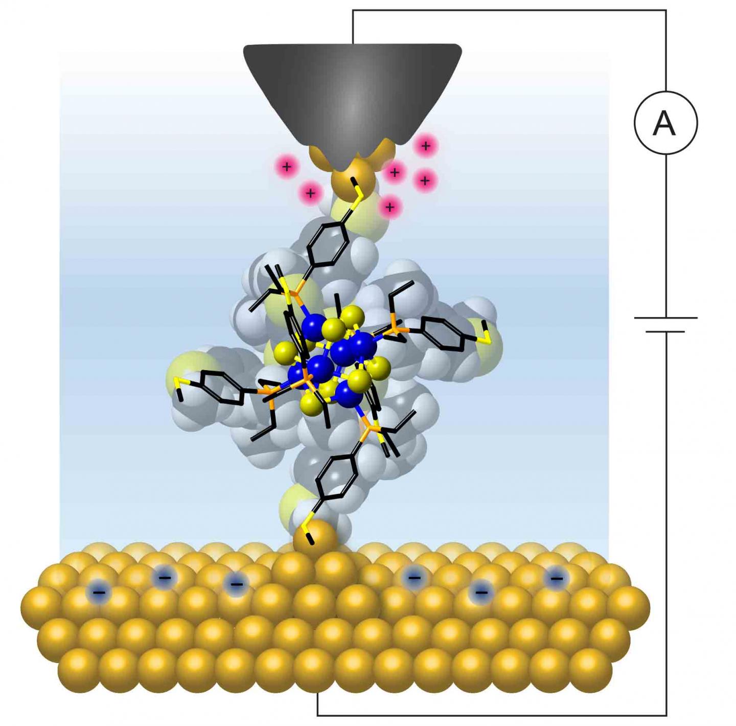
Columbia researchers wired a single molecule consisting of 14 atoms connected to two gold electrodes to show that it performs as a transistor at room temperature. (credit: Bonnie Choi/Columbia University)

Columbia Engineering researchers have taken a key step toward atomically precise, reproducible transistors made from single molecules and operating at room temperature — a major goal in the field of molecular electronics.

The team created a two-terminal transistor with a diameter of about 0.5 nanometers and core consisting of just 14 atoms. The device can reliably switch from insulator to conductor when charge is added or removed, one electron at a time (known as “current blockade”).*

The research was published in the journal Nature Nanotechnology.

Controllable structure with atomic precision

“With these molecular clusters, we have complete control over their structure with atomic precision and can change the elemental composition and structure in a controllable manner to elicit certain electrical response,” says Latha Venkataraman, leader of the Columbia research team.

The researchers plan to design improved molecular cluster systems with better electrical performance (such as higher on/off current ratio and different accessible states) and increase the number of atoms in the cluster core, while maintaining the atomic precision and uniformity of the compound.

Other studies have created quantum dots to produce similar effects, but the dots are much larger and not uniform in size, and the results have not been reproducible. The ultimate size reduction would be single-atom transistors, but they require ultra-cold temperatures (minus 196 degrees Celsius in this case, for example).

The single molecule’s 14-atom core structure comprises cobalt (blue) and sulfur (yellow) atoms (left) and ethyl-4-(methylthio)phenyl phosphine atoms, used to wire the cluster into a junction (right). (credit: Bonnie Choi/Columbia University)

* The researchers used a scanning tunneling microscope technique that they pioneered to make junctions comprising a single cluster connected to the two gold electrodes, which enabled them to characterize its electrical response as they varied the applied bias voltage. The technique allows them to fabricate and measure thousands of junctions with reproducible transport characteristics. The team worked with small inorganic molecular clusters that were identical in shape and size, so they knew exactly — down to the atomic scale — what they were measuring. The team evaluated the performance of the diode by the on/off ratio — the ratio between the current flowing through the device when it is switched on and the residual current still present in its “off” state. At room temperature, they observed a high on/off ratio of about 600 in single-cluster junctions, higher than any other single-molecule devices measured to date.


Abstract of Room-temperature current blockade in atomically defined single-cluster junctions

Fabricating nanoscopic devices capable of manipulating and processing single units of charge is an essential step towards creating functional devices where quantum effects dominate transport characteristics. The archetypal single-electron transistor comprises a small conducting or semiconducting island separated from two metallic reservoirs by insulating barriers. By enabling the transfer of a well-defined number of charge carriers between the island and the reservoirs, such a device may enable discrete single-electron operations. Here, we describe a single-molecule junction comprising a redox-active, atomically precise cobalt chalcogenide cluster wired between two nanoscopic electrodes. We observe current blockade at room temperature in thousands of single-cluster junctions. Below a threshold voltage, charge transfer across the junction is suppressed. The device is turned on when the temporary occupation of the core states by a transiting carrier is energetically enabled, resulting in a sequential tunnelling process and an increase in current by a factor of ∼600. We perform in situ and ex situ cyclic voltammetry as well as density functional theory calculations to unveil a two-step process mediated by an orbital localized on the core of the cluster in which charge carriers reside before tunnelling to the collector reservoir. As the bias window of the junction is opened wide enough to include one of the cluster frontier orbitals, the current blockade is lifted and charge carriers can tunnel sequentially across the junction.

Single-molecule-level data storage may achieve 100 times higher data density

(credit: iStock)

Scientists at the University of Manchester have developed a data-storage method that could achieve 100 times higher data density than current technologies.*

The system would allow for data servers to operate at the (relatively high) temperature of -213 °C. That could make it possible in the future for data servers to be chilled by liquid nitrogen (-196 °C) — a cooling method that is relatively cheap compared to the far more expensive liquid helium (which requires -269 °C) currently used.

The research provides proof-of-concept that such technologies could be achievable in the near future “with judicious molecular design.”

Huge benefits for the environment

Molecular-level data storage could lead to much smaller hard drives that require less energy, meaning data centers across the globe could be smaller, lower-cost, and a lot more energy-efficient.

Google data centers (credit: Google)

For example, Google currently has 15 data centers around the world. They process an average of 40 million searches per second, resulting in 3.5 billion searches per day and 1.2 trillion searches per year. To deal with all that data, Google had approximately 2.5 million servers in each data center, it was reported in 2016, and that number was likely to rise.

Some reports say the energy consumed at such centers could account for as much as 2 per cent of the world’s total greenhouse gas emissions. This means any improvement in data storage and energy efficiency could also have huge benefits for the environment as well as vastly increasing the amount of information that can be stored.

The research, led by David Mills, PhD, and Nicholas Chilton, PhD, from the School of Chemistry, is published in the journal Nature. “Our aim is to achieve even higher operating temperatures in the future, ideally functioning above liquid nitrogen temperatures,” said Mills.

* The method uses single-molecule magnets, which display “hysteresis” — a magnetic memory effect that is a requirement of magnetic data storage, such as hard drives. Molecules containing lanthanide atoms have exhibited this phenomenon at the highest temperatures to date. Lanthanides are rare earth metals used in all forms of everyday electronic devices such as smartphones, tablets and laptops. The team achieved their results using the lanthanide element dysprosium.


Abstract of Molecular magnetic hysteresis at 60 kelvin in dysprosocenium

Lanthanides have been investigated extensively for potential applications in quantum information processing and high-density data storage at the molecular and atomic scale. Experimental achievements include reading and manipulating single nuclear spins, exploiting atomic clock transitions for robust qubits and, most recently, magnetic data storage in single atoms. Single-molecule magnets exhibit magnetic hysteresis of molecular origin—a magnetic memory effect and a prerequisite of data storage—and so far, lanthanide examples have exhibited this phenomenon at the highest temperatures. However, in the nearly 25 years since the discovery of single-molecule magnets, hysteresis temperatures have increased from 4 kelvin to only about 14 kelvin using a consistent magnetic field sweep rate of about 20 oersted per second, although higher temperatures have been achieved by using very fast sweep rates (for example, 30 kelvin with 200 oersted per second). Here we report a hexa-tert-butyldysprosocenium complex—[Dy(Cpttt)2][B(C6F5)4], with Cpttt = {C5H2tBu3-1,2,4} and tBu = C(CH3)3—which exhibits magnetic hysteresis at temperatures of up to 60 kelvin at a sweep rate of 22 oersted per second. We observe a clear change in the relaxation dynamics at this temperature, which persists in magnetically diluted samples, suggesting that the origin of the hysteresis is the localized metal–ligand vibrational modes that are unique to dysprosocenium. Ab initio calculations of spin dynamics demonstrate that magnetic relaxation at high temperatures is due to local molecular vibrations. These results indicate that, with judicious molecular design, magnetic data storage in single molecules at temperatures above liquid nitrogen should be possible.

A living programmable biocomputing device based on RNA

“Ribocomputing devices” ( yellow) developed by a team at the Wyss Institute can now be used by synthetic biologists to sense and interpret multiple signals in cells and logically instruct their ribosomes (blue and green) to produce different proteins. (credit: Wyss Institute at Harvard University)

Synthetic biologists at Harvard’s Wyss Institute for Biologically Inspired Engineering and associates have developed a living programmable “ribocomputing” device based on networks of precisely designed, self-assembling synthetic RNAs (ribonucleic acid). The RNAs can sense multiple biosignals and make logical decisions to control protein production with high precision.

As reported in Nature, the synthetic biological circuits could be used to produce drugs, fine chemicals, and biofuels or detect disease-causing agents and release therapeutic molecules inside the body. The low-cost diagnostic technologies may even lead to nanomachines capable of hunting down cancer cells or switching off aberrant genes.

Biological logic gates

Similar to a digital circuit, these synthetic biological circuits can process information and make logic-guided decisions, using basic logic operations — AND, OR, and NOT. But instead of detecting voltages, the decisions are based on specific chemicals or proteins, such as toxins in the environment, metabolite levels, or inflammatory signals. The specific ribocomputing parts can be readily designed on a computer.

E. coli bacteria engineered to be ribocomputing devices output a green-glowing protein when they detect a specific set of programmed RNA molecules as input signals (credit: Harvard University)

The research was performed with E. coli bacteria, which regulate the expression of a fluorescent (glowing) reporter protein when the bacteria encounter a specific complex set of intra-cellular stimuli. But the researchers believe ribocomputing devices can work with other host organisms or in extracellular settings.

Previous synthetic biological circuits have only been able to sense a handful of signals, giving them an incomplete picture of conditions in the host cell. They are also built out of different types of molecules, such as DNAs, RNAs, and proteins, that must find, bind, and work together to sense and process signals. Identifying molecules that cooperate well with one another is difficult and makes development of new biological circuits a time-consuming and often unpredictable process.

Brain-like neural networks next

Ribocomputing devices could also be freeze-dried on paper, leading to paper-based biological circuits, including diagnostics that can sense and integrate several disease-relevant signals in a clinical sample, the researchers say.

The next stage of research will focus on the use of RNA “toehold” technology* to produce neural networks within living cells — circuits capable of analyzing a range of excitatory and inhibitory inputs, averaging them, and producing an output once a particular threshold of activity is reached. (Similar to how a neuron averages incoming signals from other neurons.)

Ultimately, researchers hope to induce cells to communicate with one another via programmable molecular signals, forming a truly interactive, brain-like network, according to lead author Alex Green, an assistant professor at Arizona State University’s Biodesign Institute.

Wyss Institute Core Faculty member Peng Yin, Ph.D., who led the study, is also Professor of Systems Biology at Harvard Medical School.

The study was funded by the Wyss Institute’s Molecular Robotics Initiative, a Defense Advanced Research Projects Agency (DARPA) Living Foundries grant, and grants from the National Institute of Health (NIH), the Office of Naval Research (ONR), the National Science Foundation (NSF) and the Defense Threat Reduction Agency (DTRA).

* The team’s approach evolved from its previous development of “toehold switches” in 2014 — programmable hairpin-like nano-structures made of RNA. In principle, RNA toehold wwitches can control the production of a specific protein: when a desired complementary “trigger” RNA, which can be part of the cell’s natural RNA repertoire, is present and binds to the toehold switch, the hairpin structure breaks open. Only then will the cell’s ribosomes get access to the RNA and produce the desired protein.


Wyss Institute | Mechanism of the Toehold Switch


Abstract of Complex cellular logic computation using ribocomputing devices

Synthetic biology aims to develop engineering-driven approaches to the programming of cellular functions that could yield transformative technologies. Synthetic gene circuits that combine DNA, protein, and RNA components have demonstrated a range of functions such as bistability, oscillation, feedback, and logic capabilities. However, it remains challenging to scale up these circuits owing to the limited number of designable, orthogonal, high-performance parts, the empirical and often tedious composition rules, and the requirements for substantial resources for encoding and operation. Here, we report a strategy for constructing RNA-only nanodevices to evaluate complex logic in living cells. Our ‘ribocomputing’ systems are composed of de-novo-designed parts and operate through predictable and designable base-pairing rules, allowing the effective in silico design of computing devices with prescribed configurations and functions in complex cellular environments. These devices operate at the post-transcriptional level and use an extended RNA transcript to co-localize all circuit sensing, computation, signal transduction, and output elements in the same self-assembled molecular complex, which reduces diffusion-mediated signal losses, lowers metabolic cost, and improves circuit reliability. We demonstrate that ribocomputing devices in Escherichia coli can evaluate two-input logic with a dynamic range up to 900-fold and scale them to four-input AND, six-input OR, and a complex 12-input expression (A1 AND A2 AND NOT A1*) OR (B1 AND B2 AND NOT B2*) OR (C1 AND C2) OR (D1 AND D2) OR (E1 AND E2). Successful operation of ribocomputing devices based on programmable RNA interactions suggests that systems employing the same design principles could be implemented in other host organisms or in extracellular settings.

How to ‘talk’ to your computer or car with hand or body poses

Researchers at Carnegie Mellon University’s Robotics Institute have developed a system that can detect and understand body poses and movements of multiple people from a video in real time — including, for the first time, the pose of each individual’s fingers.

The ability to recognize finger or hand poses, for instance, will make it possible for people to interact with computers in new and more natural ways, such as simply pointing at things.

That will also allow robots to perceive you’re doing, what moods you’re in, and whether you can be interrupted, for example. Your self-driving car could get an early warning that a pedestrian is about to step into the street by monitoring your body language. The technology could also be used for behavioral diagnosis and rehabilitation for conditions such as autism, dyslexia, and depression, the researchers say.

This new method was developed at CMU’s NSF-funded Panoptic Studio, a two-story dome embedded with 500 video cameras, but the researchers can now do the same thing with a single camera and laptop computer.

The researchers have released their computer code. It’s already being widely used by research groups, and more than 20 commercial groups, including automotive companies, have expressed interest in licensing the technology, according to Yaser Sheikh, associate professor of robotics.

Tracking multiple people in real time, particularly in social situations where they may be in contact with each other, presents a number of challenges. Sheikh and his colleagues took a bottom-up approach, which first localizes all the body parts in a scene — arms, legs, faces, etc. — and then associates those parts with particular individuals.

Sheikh and his colleagues will present reports on their multiperson and hand-pose detection methods at CVPR 2017, the Computer Vision and Pattern Recognition Conference, July 21–26 in Honolulu.

Radical new vertically integrated 3D chip design combines computing and data storage

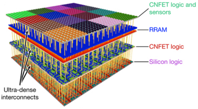
Four vertical layers in new 3D nanosystem chip. Top (fourth layer): sensors and more than one million carbon-nanotube field-effect transistor (CNFET) logic inverters; third layer, on-chip non-volatile RRAM (1 Mbit memory); second layer, CNFET logic with classification accelerator (to identify sensor inputs); first (bottom) layer, silicon FET logic. (credit: Max M. Shulaker et al./Nature)

A radical new 3D chip that combines computation and data storage in vertically stacked layers — allowing for processing and storing massive amounts of data at high speed in future transformative nanosystems — has been designed by researchers at Stanford University and MIT.

The new 3D-chip design* replaces silicon with carbon nanotubes (sheets of 2-D graphene formed into nanocylinders) and integrates resistive random-access memory (RRAM) cells.

Carbon-nanotube field-effect transistors (CNFETs) are an emerging transistor technology that can scale beyond the limits of silicon MOSFETs (conventional chips), and promise an order-of-magnitude improvement in energy-efficient computation. However, experimental demonstrations of CNFETs so far have been small-scale and limited to integrating only tens or hundreds of devices (see earlier 2015 Stanford research, “Skyscraper-style carbon-nanotube chip design…”).

The researchers integrated more than 1 million RRAM cells and 2 million carbon-nanotube field-effect transistors in the chip, making it the most complex nanoelectronic system ever made with emerging nanotechnologies, according to the researchers. RRAM is an emerging memory technology that promises high-capacity, non-volatile data storage, with improved speed, energy efficiency, and density, compared to dynamic random-access memory (DRAM).

Instead of requiring separate components, the RRAM cells and carbon nanotubes are built vertically over one another, creating a dense new 3D computer architecture** with interleaving layers of logic and memory. By using ultradense through-chip vias (electrical interconnecting wires passing between layers), the high delay with conventional wiring between computer components is eliminated.

The new 3D nanosystem can capture massive amounts of data every second, store it directly on-chip, perform in situ processing of the captured data, and produce “highly processed” information. “Such complex nanoelectronic systems will be essential for future high-performance, highly energy-efficient electronic systems,” the researchers say.

How to combine computation and storage

Illustration of separate CPU (bottom) and RAM memory (top) in current computer architecture (images credit: iStock)

The new chip design aims to replace current chip designs, which separate computing and data storage, resulting in limited-speed connections.

Separate 2D chips have been required because “building conventional silicon transistors involves extremely high temperatures of over 1,000 degrees Celsius,” explains lead author Max Shulaker, an assistant professor of electrical engineering and computer science at MIT and lead author of a paper published July 5, 2017 in the journal Nature. “If you then build a second layer of silicon circuits on top, that high temperature will damage the bottom layer of circuits.”

Instead, carbon nanotube circuits and RRAM memory can be fabricated at much lower temperatures: below 200 C. “This means they can be built up in layers without harming the circuits beneath,” says Shulaker.

Overcoming communication and computing bottlenecks

As applications analyze increasingly massive volumes of data, the limited rate at which data can be moved between different chips is creating a critical communication “bottleneck.” And with limited real estate on increasingly miniaturized chips, there is not enough room to place chips side-by-side.

At the same time, embedded intelligence in areas ranging from autonomous driving to personalized medicine is now generating huge amounts of data, but silicon transistors are no longer improving at the historic rate that they have for decades.

Instead, three-dimensional integration is the most promising approach to continue the technology-scaling path set forth by Moore’s law, allowing an increasing number of devices to be integrated per unit volume, according to Jan Rabaey, a professor of electrical engineering and computer science at the University of California at Berkeley, who was not involved in the research.

Three-dimensional integration “leads to a fundamentally different perspective on computing architectures, enabling an intimate interweaving of memory and logic,” he says. “These structures may be particularly suited for alternative learning-based computational paradigms such as brain-inspired systems and deep neural nets, and the approach presented by the authors is definitely a great first step in that direction.”

The new 3D design provides several benefits for future computing systems, including:

  • Logic circuits made from carbon nanotubes can be an order of magnitude more energy-efficient compared to today’s logic made from silicon.
  • RRAM memory is denser, faster, and more energy-efficient compared to conventional DRAM (dynamic random-access memory) devices.
  • The dense through-chip vias (wires) can enable vertical connectivity that is 1,000 times more dense than conventional packaging and chip-stacking solutions allow, which greatly improves the data communication bandwidth between vertically stacked functional layers. For example, each sensor in the top layer can connect directly to its respective underlying memory cell with an inter-layer via. This enables the sensors to write their data in parallel directly into memory and at high speed.
  • The design is compatible in both fabrication and design with today’s CMOS silicon infrastructure.

Shulaker next plans to work with Massachusetts-based semiconductor company Analog Devices to develop new versions of the system.

This work was funded by the Defense Advanced Research Projects Agency, the National Science Foundation, Semiconductor Research Corporation, STARnet SONIC, and member companies of the Stanford SystemX Alliance.

* As a working-prototype demonstration of the potential of the technology, the researchers took advantage of the ability of carbon nanotubes to also act as sensors. On the top layer of the chip, they placed more than 1 million carbon nanotube-based sensors, which they used to detect and classify ambient gases for detecting signs of disease by sensing particular compounds in a patient’s breath, says Shulaker. By layering sensing, data storage, and computing, the chip was able to measure each of the sensors in parallel, and then write directly into its memory, generating huge bandwidth in just one device, according to Shulaker. The top layer could be replaced with additional computation or data storage subsystems, or with other forms of input/output, he explains.

** Previous R&D in 3D chip technologies and their limitations are covered here, noting that “in general, 3D integration is a broad term that includes such technologies as 3D wafer-level packaging (3DWLP); 2.5D and 3D interposer-based integration; 3D stacked ICs (3D-SICs), monolithic 3D ICs; 3D heterogeneous integration; and 3D systems integration.” The new Stanford-MIT nanosystem design significantly expands this definition.


Abstract of Three-dimensional integration of nanotechnologies for computing and data storage on a single chip

The computing demands of future data-intensive applications will greatly exceed the capabilities of current electronics, and are unlikely to be met by isolated improvements in transistors, data storage technologies or integrated circuit architectures alone. Instead, transformative nanosystems, which use new nanotechnologies to simultaneously realize improved devices and new integrated circuit architectures, are required. Here we present a prototype of such a transformative nanosystem. It consists of more than one million resistive random-access memory cells and more than two million carbon-nanotube field-effect transistors—promising new nanotechnologies for use in energy-efficient digital logic circuits and for dense data storage—fabricated on vertically stacked layers in a single chip. Unlike conventional integrated circuit architectures, the layered fabrication realizes a three-dimensional integrated circuit architecture with fine-grained and dense vertical connectivity between layers of computing, data storage, and input and output (in this instance, sensing). As a result, our nanosystem can capture massive amounts of data every second, store it directly on-chip, perform in situ processing of the captured data, and produce ‘highly processed’ information. As a working prototype, our nanosystem senses and classifies ambient gases. Furthermore, because the layers are fabricated on top of silicon logic circuitry, our nanosystem is compatible with existing infrastructure for silicon-based technologies. Such complex nano-electronic systems will be essential for future high-performance and highly energy-efficient electronic systems.

Graphene-based computer would be 1,000 times faster than silicon-based, use 100th the power

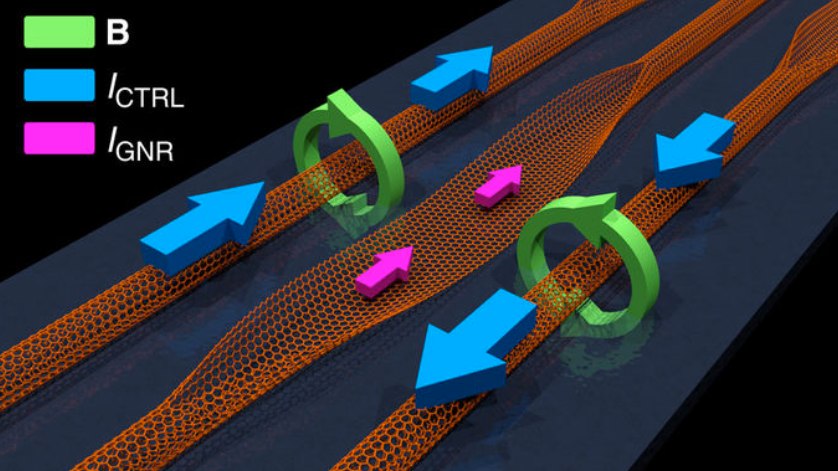
How a graphene-based transistor would work. A graphene nanoribbon (GNR) is created by unzipping (opening up) a portion of a carbon nanotube (CNT) (the flat area, shown with pink arrows above it). The GRN switching is controlled by two surrounding parallel CNTs. The magnitudes and relative directions of the control current, ICTRL (blue arrows) in the CNTs determine the rotation direction of the magnetic fields, B (green). The magnetic fields then control the GNR magnetization (based on the recent discovery of negative magnetoresistance), which causes the GNR to switch from resistive (no current) to conductive, resulting in current flow, IGNR (pink arrows) — in other words, causing the GNR to act as a transistor gate. The magnitude of the current flow through the GNR functions as the binary gate output — with binary 1 representing the current flow of the conductive state and binary 0 representing no current (the resistive state). (credit: Joseph S. Friedman et al./Nature Communications)

A future graphene-based transistor using spintronics could lead to tinier computers that are a thousand times faster and use a hundredth of the power of silicon-based computers.

The radical transistor concept, created by a team of researchers at Northwestern University, The University of Texas at Dallas, University of Illinois at Urbana-Champaign, and University of Central Florida, is explained this month in an open-access paper in the journal Nature Communications.

Transistors act as on and off switches. A series of transistors in different arrangements act as logic gates, allowing microprocessors to solve complex arithmetic and logic problems. But the speed of computer microprocessors that rely on silicon transistors has been relatively stagnant since around 2005, with clock speeds mostly in the 3 to 4 gigahertz range.

Clock speeds approaching the terahertz range

The researchers discovered that by applying a magnetic field to a graphene ribbon (created by unzipping a carbon nanotube), they could change the resistance of current flowing through the ribbon. The magnetic field — controlled by increasing or decreasing the current through adjacent carbon nanotubes — increased or decreased the flow of current.

A cascading series of graphene transistor-based logic circuits could produce a massive jump, with clock speeds approaching the terahertz range — a thousand times faster.* They would also be smaller and substantially more efficient, allowing device-makers to shrink technology and squeeze in more functionality, according to Ryan M. Gelfand, an assistant professor in The College of Optics & Photonics at the University of Central Florida.

The researchers hope to inspire the fabrication of these cascaded logic circuits to stimulate a future transformative generation of energy-efficient computing.

* Unlike other spintronic logic proposals, these new logic gates can be cascaded directly through the carbon materials without requiring intermediate circuits and amplification between gates. That would result in compact circuits with reduced area that are far more efficient than with CMOS switching, which is limited by charge transfer and accumulation from RLC (resistance-inductance-capacitance) interconnect delays.


Abstract of Cascaded spintronic logic with low-dimensional carbon

Remarkable breakthroughs have established the functionality of graphene and carbon nanotube transistors as replacements to silicon in conventional computing structures, and numerous spintronic logic gates have been presented. However, an efficient cascaded logic structure that exploits electron spin has not yet been demonstrated. In this work, we introduce and analyse a cascaded spintronic computing system composed solely of low-dimensional carbon materials. We propose a spintronic switch based on the recent discovery of negative magnetoresistance in graphene nanoribbons, and demonstrate its feasibility through tight-binding calculations of the band structure. Covalently connected carbon nanotubes create magnetic fields through graphene nanoribbons, cascading logic gates through incoherent spintronic switching. The exceptional material properties of carbon materials permit Terahertz operation and two orders of magnitude decrease in power-delay product compared to cutting-edge microprocessors. We hope to inspire the fabrication of these cascaded logic circuits to stimulate a transformative generation of energy-efficient computing.

High-speed light-based systems could replace supercomputers for certain ‘deep learning’ calculations

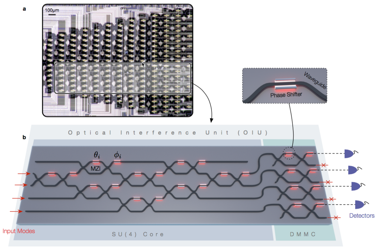
(a) Optical micrograph of an experimentally fabricated on-chip optical interference unit; the physical region where the optical neural network program exists is highlighted in gray. A programmable nanophotonic processor uses a field-programmable gate array (similar to an FPGA integrated circuit ) — an array of interconnected waveguides, allowing the light beams to be modified as needed for a specific deep-learning matrix computation. (b) Schematic illustration of the optical neural network program, which performs matrix multiplication and amplification fully optically. (credit: Yichen Shen et al./Nature Photonics)

A team of researchers at MIT and elsewhere has developed a new approach to deep learning systems — using light instead of electricity, which they say could vastly improve the speed and efficiency of certain deep-learning computations.

Deep-learning systems are based on artificial neural networks that mimic the way the brain learns from an accumulation of examples. They can enable technologies such as face- and voice-recognition software, or scour vast amounts of medical data to find patterns that could be useful diagnostically, for example.

But the computations these systems carry out are highly complex and demanding, even for supercomputers. Traditional computer architectures are not very efficient for calculations needed for neural-network tasks that involve repeated multiplications of matrices (arrays of numbers). These can be computationally intensive for conventional CPUs or even GPUs.

Programmable nanophotonic processor

Instead, the new approach uses an optical device that the researchers call a “programmable nanophotonic processor.” Multiple light beams are directed in such a way that their waves interact with each other, producing interference patterns that “compute” the intended operation.

The optical chips using this architecture could, in principle, carry out dense matrix multiplications (the most power-hungry and time-consuming part in AI algorithms) for learning tasks much faster, compared to conventional electronic chips. The researchers expect a computational speed enhancement of at least two orders of magnitude over the state-of-the-art and three orders of magnitude in power efficiency.

“This chip, once you tune it, can carry out matrix multiplication with, in principle, zero energy, almost instantly,” says Marin Soljacic, one of the MIT researchers on the team.

To demonstrate the concept, the team set the programmable nanophotonic processor to implement a neural network that recognizes four basic vowel sounds. Even with the prototype system, they were able to achieve a 77 percent accuracy level, compared to about 90 percent for conventional systems. There are “no substantial obstacles” to scaling up the system for greater accuracy, according to Soljacic.

The team says is will still take a lot more time and effort to make this system useful. However, once the system is scaled up and fully functioning, the low-power system should find many uses, especially for situations where power is limited, such as in self-driving cars, drones, and mobile consumer devices. Other uses include signal processing for data transmission and computer centers.

The research was published Monday (June 12, 2017) in a paper in the journal Nature Photonics (open-access version available on arXiv).

The team also included researchers at Elenion Technologies of New York and the Université de Sherbrooke in Quebec. The work was supported by the U.S. Army Research Office through the Institute for Soldier Nanotechnologies, the National Science Foundation, and the Air Force Office of Scientific Research.


Abstract of Deep learning with coherent nanophotonic circuits

Artificial neural networks are computational network models inspired by signal processing in the brain. These models have dramatically improved performance for many machine-learning tasks, including speech and image recognition. However, today’s computing hardware is inefficient at implementing neural networks, in large part because much of it was designed for von Neumann computing schemes. Significant effort has been made towards developing electronic architectures tuned to implement artificial neural networks that exhibit improved computational speed and accuracy. Here, we propose a new architecture for a fully optical neural network that, in principle, could offer an enhancement in computational speed and power efficiency over state-of-the-art electronics for conventional inference tasks. We experimentally demonstrate the essential part of the concept using a programmable nanophotonic processor featuring a cascaded array of 56 programmable Mach–Zehnder interferometers in a silicon photonic integrated circuit and show its utility for vowel recognition.

Princeton/Adobe technology will let you edit voices like text

Technology developed by Princeton University computer scientists may do for audio recordings of the human voice what word processing software did for the written word and Adobe Photoshop did for images.

“VoCo” software, still in the research stage, makes it easy to add or replace a word in an audio recording of a human voice by simply editing a text transcript of the recording. New words are automatically synthesized in the speaker’s voice — even if they don’t appear anywhere else in the recording.

The system uses a sophisticated algorithm to learn and recreate the sound of a particular voice. It could one day make editing podcasts and narration in videos much easier, or in the future, create personalized robotic voices that sound natural, according to co-developer Adam Finkelstein, a professor of computer science at Princeton. Or people who have lost their voices due to injury or disease might be able to recreate their voices through a robotic system, but one that sounds natural.

An earlier version of VoCo was announced in November 2016. A paper describing the current VoCo development will be published in the July issue of the journal Transactions on Graphics (an open-access preprint is available).


How it works (technical description)

VoCo allows people to edit audio recordings with the ease of changing words on a computer screen. The system inserts new words in the same voice as the rest of the recording. (credit: Professor Adam Finkelstein)

VoCo’s user interface looks similar to other audio editing software such as the podcast editing program Audacity, with a waveform of the audio track and cut, copy and paste tools for editing. But VoCo also augments the waveform with a text transcript of the track and allows the user to replace or insert new words that don’t already exist in the track by simply typing in the transcript. When the user types the new word, VoCo updates the audio track, automatically synthesizing the new word by stitching together snippets of audio from elsewhere in the narration.

VoCo is is based on an optimization algorithm that searches the voice recording and chooses the best possible combinations of phonemes (partial word sounds) to build new words in the user’s voice. To do this, it needs to find the individual phonemes and sequences of them that stitch together without abrupt transitions. It also needs to be fitted into the existing sentence so that the new word blends in seamlessly. Words are pronounced with different emphasis and intonation depending on where they fall in a sentence, so context is important.

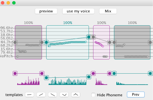
Advanced VoCo editors can manually adjust pitch profile, amplitude and snippet duration. Novice users can choose from a predefined set of pitch profiles (bottom), or record their own voice as an exemplar to control pitch and timing (top). (credit: Professor Adam Finkelstein)

For clues about this context, VoCo looks to an audio track of the sentence that is automatically synthesized in artificial voice from the text transcript — one that sounds robotic to human ears. This recording is used as a point of reference in building the new word. VoCo then matches the pieces of sound from the real human voice recording to match the word in the synthesized track — a technique known as “voice conversion,” which inspired the project name, VoCo.

In case the synthesized word isn’t quite right, VoCo offers users several versions of the word to choose from. The system also provides an advanced editor to modify pitch and duration, allowing expert users to further polish the track.

To test how effective their system was a producing authentic sounding edits, the researchers asked people to listen to a set of audio tracks, some of which had been edited with VoCo and other that were completely natural. The fully automated versions were mistaken for real recordings more than 60 percent of the time.

The Princeton researchers are currently refining the VoCo algorithm to improve the system’s ability to integrate synthesized words more smoothly into audio tracks. They are also working to expand the system’s capabilities to create longer phrases or even entire sentences synthesized from a narrator’s voice.


Fake news videos?

Disney Research’s FaceDirector allows for editing recorded facial expressions and voice into a video (credit: Disney Research)

A key use for VoCo might be in intelligent personal assistants like Apple’s Siri, Google Assistant, Amazon’s Alexa, and Microsoft’s Cortana, or for using movie actors’ voices from old films in new ones, Finkelstein suggests.

But there are obvious concerns about fraud. It might even be possible to create a convincing fake video. Video clips with different facial expressions and lip movements (using Disney Research’s FaceDirector, for example) could be edited in and matched to associated fake words and other audio (such as background noise and talking), along with green screen to create fake backgrounds.

With billions of people now getting their news online and unfiltered, augmented-reality coming, and hacking way out of control, things may get even weirder. …

Zeyu Jin, a Princeton graduate student advised by Finkelstein, will present the work at the Association for Computing Machinery SIGGRAPH conference in July. The work at Princeton was funded by the Project X Fund, which provides seed funding to engineers for pursuing speculative projects. The Princeton researchers collaborated with scientists Gautham Mysore, Stephen DiVerdi, and Jingwan Lu at Adobe Research. Adobe has not announced availability of a commercial version of VoCo, or plans to integrate VoCo into Adobe Premiere Pro (or FaceDirector).


Abstract of VoCo: Text-based Insertion and Replacement in Audio Narration

Editing audio narration using conventional software typically involves many painstaking low-level manipulations. Some state of the art systems allow the editor to work in a text transcript of the narration, and perform select, cut, copy and paste operations directly in the transcript; these operations are then automatically applied to the waveform in a straightforward manner. However, an obvious gap in the text-based interface is the ability to type new words not appearing in the transcript, for example inserting a new word for emphasis or replacing a misspoken word. While high-quality voice synthesizers exist today, the challenge is to synthesize the new word in a voice that matches the rest of the narration. This paper presents a system that can synthesize a new word or short phrase such that it blends seamlessly in the context of the existing narration. Our approach is to use a text to speech synthesizer to say the word in a generic voice, and then use voice conversion to convert it into a voice that matches the narration. Offering a range of degrees of control to the editor, our interface supports fully automatic synthesis, selection among a candidate set of alternative pronunciations, fine control over edit placements and pitch profiles, and even guidance by the editors own voice. The paper presents studies showing that the output of our method is preferred over baseline methods and often indistinguishable from the original voice.