Controlling acoustic properties with algorithms and computational methods

A “zoolophone” with animal shapes automatically created using a computer algorithm. The tone of each key is comparable to those of professionally made instruments as a demonstration of an algorithm for computationally designing an object’s vibrational properties and sounds. (Changxi Zheng/Columbia Engineering)

Computer scientists at Columbia Engineering, Harvard, and MIT have demonstrated that acoustic properties — both sound and vibration — can be controlled by 3D-printing specific shapes.

They designed an optimization algorithm and used computational methods and digital fabrication to alter the shape of 2D and 3D objects, creating what looks to be a simple children’s musical instrument — a xylophone with keys in the shape of zoo animals.

Practical uses

“Our discovery could lead to a wealth of possibilities that go well beyond musical instruments,” says Changxi Zheng, assistant professor of computer science at Columbia Engineering, who led the research team.

“Our algorithm could lead to ways to build less noisy computer fans and bridges that don’t amplify vibrations under stress, and advance the construction of micro-electro-mechanical resonators whose vibration modes are of great importance.”

Zheng, who works in the area of dynamic, physics-based computational sound for immersive environments, wanted to see if he could use computation and digital fabrication to actively control the acoustical property, or vibration, of an object.

Zheng’s team decided to focus on simplifying the slow, complicated, manual process of designing “idiophones” — musical instruments that produce sounds through vibrations in the instrument itself, not through strings or reeds.

The surface vibration and resulting sounds depend on the idiophone’s shape in a complex way, so designing the shapes to obtain desired sound characteristics is not straightforward, and their forms have so far been limited to well-understood designs such as bars that are tuned by careful drilling of dimples on the underside of the instrument.

Optimizing sound properties

To demonstrate their new technique, the team settled on building a “zoolophone,” a metallophone with playful animal shapes (a metallophone is an idiophone made of tuned metal bars that can be struck to make sound, such as a glockenspiel).

Their algorithm optimized and 3D-printed the instrument’s keys in the shape of colorful lions, turtles, elephants, giraffes, and more, modelling the geometry to achieve the desired pitch and amplitude of each part.

“Our zoolophone’s keys are automatically tuned to play notes on a scale with overtones and frequency of a professionally produced xylophone,” says Zheng, whose team spent nearly two years on developing new computational methods while borrowing concepts from computer graphics, acoustic modeling, mechanical engineering, and 3D printing.

“By automatically optimizing the shape of 2D and 3D objects through deformation and perforation, we were able to produce such professional sounds that our technique will enable even novices to design metallophones with unique sound and appearance.”

3D metallophone cups automatically created by computers (credit: Changxi Zheng/Columbia Engineering)

The zoolophone represents fundamental research into understanding the complex relationships between an object’s geometry and its material properties, and the vibrations and sounds it produces when struck.

While previous algorithms attempted to optimize either amplitude (loudness) or frequency, the zoolophone required optimizing both simultaneously to fully control its acoustic properties. Creating realistic musical sounds required more work to add in overtones, secondary frequencies higher than the main one that contribute to the timbre associated with notes played on a professionally produced instrument.

Looking for the most optimal shape that produces the desired sound when struck proved to be the core computational difficulty: the search space for optimizing both amplitude and frequency is immense. To increase the chances of finding the most optimal shape, Zheng and his colleagues developed a new, fast stochastic optimization method, which they called Latin Complement Sampling (LCS).

They input shape and user-specified frequency and amplitude spectra (for instance, users can specify which shapes produce which note) and, from that information, optimized the shape of the objects through deformation and perforation to produce the wanted sounds. LCS outperformed all other alternative optimizations and can be used in a variety of other problems.

“Acoustic design of objects today remains slow and expensive,” Zheng notes. “We would like to explore computational design algorithms to improve the process for better controlling an object’s acoustic properties, whether to achieve desired sound spectra or to reduce undesired noise. This project underscores our first step toward this exciting direction in helping us design objects in a new way.”

Zheng, whose previous work in computer graphics includes synthesizing realistic sounds that are automatically synchronized to simulated motions, has already been contacted by researchers interested in applying his approach to micro-electro-mechanical systems (MEMS), in which vibrations filter RF signals.

Their work—“Computational Design of Metallophone Contact Sounds”—will be presented at SIGGRAPH Asia on November 4 in Kobe, Japan.

The work at Columbia Engineering was supported in part by the National Science Foundation (NSF) and Intel, at Harvard and MIT by NSF, Air Force Research Laboratory, and DARPA.


A new way to create spintronic magnetic information storage

A magnetized cobalt disk (red) placed atop a thin cobalt-palladium film (light purple background) can be made to confer its own ringed configuration of magnetic moments (orange arrows) to the film below, creating a skyrmion in the film (purple arrows). The skyrmion might be usable in computer data storage systems. (credit: Dustin Gilbert / NIST)

Exotic ring-shaped magnetic effects called “skyrmions*” could be the basis for a new type of nonvolatile magnetic computer data storage, replacing current hard-drive technology, according to a team of researchers at the National Institute of Standards and Technology (NIST) and several universities.

Skyrmions have the advantage of operating at magnetic fields that are several orders of magnitude weaker, but have worked at only very low temperatures until now. The research breakthrough was the discovery of a practical way to create and access magnetic skyrmions, and under ambient room-temperature conditions.

The skrymion effect refers to extreme conditions in which certain magnetic materials can develop spots where the magnetic moments** curve and twist, forming a winding, ring-like configuration. To achieve that, the physicists placed arrays of tiny magnetized cobalt disks atop a thin film made of cobalt and palladium. That protects them from outside influence, meaning the data they store would not be corrupted easily.

But “seeing” these skyrmion configurations underneath was a challenge. The team solved that by using neutrons to see through the disk.

That discovery has implications for spintronics (using magnetic spin to store data). “The advantage [with skyrmions] is that you’d need way less power to push them around than any other method proposed for spintronics,” said NIST’s Dustin Gilbert. “What we need to do next is figure out how to make them move around.”

Physicists at the University of California, Davis; University of Maryland, College Park; University of California, Santa Cruz; and Lawrence Berkeley National Laboratory were also involved in the study.

* Named after the physicist who proposed them. 

** The force that a magnet can exert on electric currents and the torque that a magnetic field will exert on it.


Abstract of Realization of ground-state artificial skyrmion lattices at room temperature

The topological nature of magnetic skyrmions leads to extraordinary properties that provide new insights into fundamental problems of magnetism and exciting potentials for novel magnetic technologies. Prerequisite are systems exhibiting skyrmion lattices at ambient conditions, which have been elusive so far. Here, we demonstrate the realization of artificial Bloch skyrmion lattices over extended areas in their ground state at room temperature by patterning asymmetric magnetic nanodots with controlled circularity on an underlayer with perpendicular magnetic anisotropy (PMA). Polarity is controlled by a tailored magnetic field sequence and demonstrated in magnetometry measurements. The vortex structure is imprinted from the dots into the interfacial region of the underlayer via suppression of the PMA by a critical ion-irradiation step. The imprinted skyrmion lattices are identified directly with polarized neutron reflectometry and confirmed by magnetoresistance measurements. Our results demonstrate an exciting platform to explore room-temperature ground-state skyrmion lattices.

Gartner identifies the top 10 strategic IT technology trends for 2016

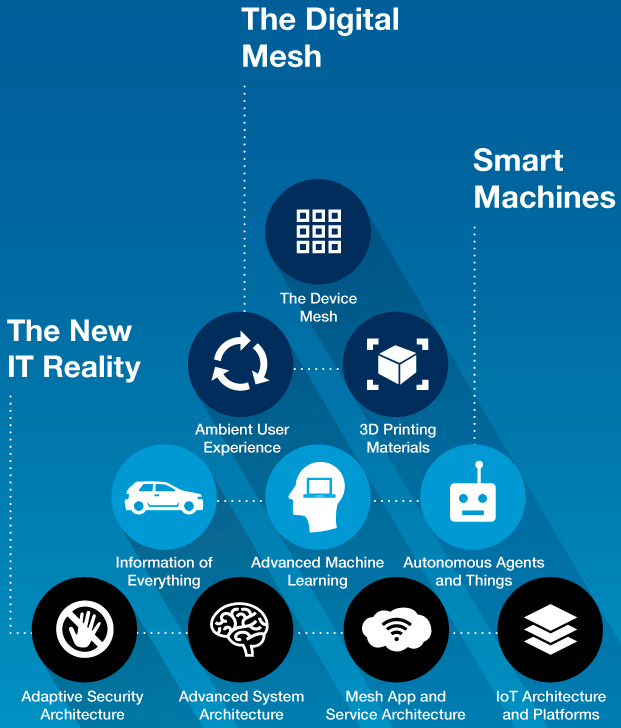
Top 10 strategic trends 2016 (credit: Gartner, Inc.)

At the Gartner Symposium/ITxpo today (Oct. 8), Gartner, Inc. highlighted the top 10 technology trends that will be strategic for most organizations in 2016 and will shape digital business opportunities through 2020.

The Device Mesh

The device mesh refers to how people access applications and information or interact with people, social communities, governments and businesses. It includes mobile devices, wearable, consumer and home electronic devices, automotive devices, and environmental devices, such as sensors in the Internet of Things (IoT), allowing for greater cooperative interaction between devices.

Ambient User Experience

The device mesh creates the foundation for a new continuous and ambient user experience. Immersive environments delivering augmented and virtual reality hold significant potential but are only one aspect of the experience. The ambient user experience preserves continuity across boundaries of device mesh, time and space. The experience seamlessly flows across a shifting set of devices — such as sensors, cars, and even factories — and interaction channels blending physical, virtual and electronic environment as the user moves from one place to another.

3D Printing Materials

Advances in 3D printing will drive user demand and a compound annual growth rate of 64.1 percent for enterprise 3D-printer shipments through 2019, which will require a rethinking of assembly line and supply chain processes to exploit 3D printing.

Information of Everything

Everything in the digital mesh produces, uses and transmits information, including sensory and contextual information. “Information of everything” addresses this influx with strategies and technologies to link data from all these different data sources. Advances in semantic tools such as graph databases as well as other emerging data classification and information analysis techniques will bring meaning to the often chaotic deluge of information.

Advanced Machine Learning

In advanced machine learning, deep neural nets (DNNs) move beyond classic computing and information management to create systems that can autonomously learn to perceive the world on their own, making it possible to address key challenges related to the information of everything trend.

DNNs (an advanced form of machine learning particularly applicable to large, complex datasets) is what makes smart machines appear “intelligent.” DNNs enable hardware- or software-based machines to learn for themselves all the features in their environment, from the finest details to broad sweeping abstract classes of content. This area is evolving quickly, and organizations must assess how they can apply these technologies to gain competitive advantage.

Autonomous Agents and Things

Machine learning gives rise to a spectrum of smart machine implementations — including robots, autonomous vehicles, virtual personal assistants (VPAs) and smart advisors — that act in an autonomous (or at least semiautonomous) manner.

VPAs such as Google Now, Microsoft’s Cortana, and Apple’s Siri are becoming smarter and are precursors to autonomous agents. The emerging notion of assistance feeds into the ambient user experience in which an autonomous agent becomes the main user interface. Instead of interacting with menus, forms and buttons on a smartphone, the user speaks to an app, which is really an intelligent agent.

Adaptive Security Architecture

The complexities of digital business and the algorithmic economy combined with an emerging “hacker industry” significantly increase the threat surface for an organization. Relying on perimeter defense and rule-based security is inadequate, especially as organizations exploit more cloud-based services and open APIs for customers and partners to integrate with their systems. IT leaders must focus on detecting and responding to threats, as well as more traditional blocking and other measures to prevent attacks. Application self-protection, as well as user and entity behavior analytics, will help fulfill the adaptive security architecture.

Advanced System Architecture

The digital mesh and smart machines require intense computing architecture demands to make them viable for organizations. Providing this required boost are high-powered and ultraefficient neuromorphic (brain-like) architectures fueled by GPUs (graphic processing units) and field-programmable gate arrays (FPGAs). There are significant gains to this architecture, such as being able to run at speeds of greater than a teraflop with high-energy efficiency.

Mesh App and Service Architecture

Monolithic, linear application designs (e.g., the three-tier architecture) are giving way to a more loosely coupled integrative approach: the apps and services architecture. Enabled by software-defined application services, this new approach enables Web-scale performance, flexibility and agility. Microservice architecture is an emerging pattern for building distributed applications that support agile delivery and scalable deployment, both on-premises and in the cloud. Containers are emerging as a critical technology for enabling agile development and microservice architectures. Bringing mobile and IoT elements into the app and service architecture creates a comprehensive model to address back-end cloud scalability and front-end device mesh experiences. Application teams must create new modern architectures to deliver agile, flexible and dynamic cloud-based applications that span the digital mesh.

Internet of Things Platforms

IoT platforms complement the mesh app and service architecture. The management, security, integration and other technologies and standards of the IoT platform are the base set of capabilities for building, managing, and securing elements in the IoT. The IoT is an integral part of the digital mesh and ambient user experience and the emerging and dynamic world of IoT platforms is what makes them possible.

* Gartner defines a strategic technology trend as one with the potential for significant impact on the organization. Factors that denote significant impact include a high potential for disruption to the business, end users or IT, the need for a major investment, or the risk of being late to adopt. These technologies impact the organization’s long-term plans, programs and initiatives.

First two-qubit logic gate built in silicon

Artist’s impression of the two-qubit logic gate device developed at UNSW. Each of the two electron qubits (red and blue) has a spin, or magnetic field, indicated by the arrow directions. Metal electrodes on the surface are used to manipulate the qubits, which interact to create an entangled quantum state. (credit: Tony Melov/UNSW)

University of New South Wales (UNSW) and Keio University engineers have built the first quantum logic gate in silicon, making calculations between two qubits* of information possible and clearing the final hurdle to making silicon quantum computers a reality.

The significant advance appears today (Oct. 5, 2015) in the journal Nature.

“What we have is a game changer,” said team leader Andrew Dzurak, Scientia Professor and Director of the Australian National Fabrication Facility at UNSW. “Because we use essentially the same device technology as existing computer chips, we believe it will be much easier to manufacture a full-scale processor chip than for any of the leading designs, which rely on more exotic technologies.”


University of New South Wales

“If quantum computers are to become a reality, the ability to conduct one- and two-qubits calculations are essential,” said Dzurak, who jointly led the team in 2012 that demonstrated the first ever silicon qubit, also reported in Nature.

Until now, using silicon, it had not been possible to make two quantum bits “talk” to each other and thereby create a logic gate. The new result means that all of the physical building blocks for a silicon-based quantum computer have now been successfully constructed, allowing engineers to finally begin the task of designing and building a functioning quantum computer, the researchers say.

Dzurak noted that the team had recently “patented a design for a full-scale quantum computer chip that would allow for millions of our qubits … using standard industrial manufacturing techniques to build the world’s first quantum processor chip. … That has major implications for the finance, security, and healthcare sectors.”

He said that a key next step for the project is to identify the right industry partners to work with to manufacture the full-scale quantum processor chip.

Dzurak’s research is supported by the Australian Research Council via the Centre of Excellence for Quantum Computation and Communication Technology, the U.S. Army Research Office, the State Government of New South Wales in Australia, the Commonwealth Bank of Australia, and the University of New South Wales. Veldhorst acknowledges support from the Netherlands Organisation for Scientific Research. The quantum logic devices were constructed at the Australian National Fabrication Facility, which is supported by the federal government’s National Collaborative Research Infrastructure Strategy (NCRIS).

* In classical computers, data is rendered as binary bits, which are always in one of two states: 0 or 1. A quantum bit (or ‘qubit’) can exist in both of these states at once, a condition known as a superposition. A qubit operation exploits this quantum weirdness by allowing many computations to be performed in parallel (a two-qubit system performs the operation on 4 values, a three-qubit system on 8, and so on).


Abstract of A two-qubit logic gate in silicon

Quantum computation requires qubits that can be coupled in a scalable manner, together with universal and high-fidelity one- and two-qubit logic gates. Many physical realizations of qubits exist, including single photons, trapped ions, superconducting circuits, single defects or atoms in diamond and silicon, and semiconductor quantum dots, with single-qubit fidelities that exceed the stringent thresholds required for fault-tolerant quantum computing. Despite this, high-fidelity two-qubit gates in the solid state that can be manufactured using standard lithographic techniques have so far been limited to superconducting qubits, owing to the difficulties of coupling qubits and dephasing in semiconductor systems. Here we present a two-qubit logic gate, which uses single spins in isotopically enriched silicon and is realized by performing single- and two-qubit operations in a quantum dot system using the exchange interaction, as envisaged in the Loss–DiVincenzo proposal. We realize CNOT gates via controlled-phase operations combined with single-qubit operations. Direct gate-voltage control provides single-qubit addressability, together with a switchable exchange interaction that is used in the two-qubit controlled-phase gate. By independently reading out both qubits, we measure clear anticorrelations in the two-spin probabilities of the CNOT gate.

Method to replace silicon with carbon nanotubes developed by IBM Research

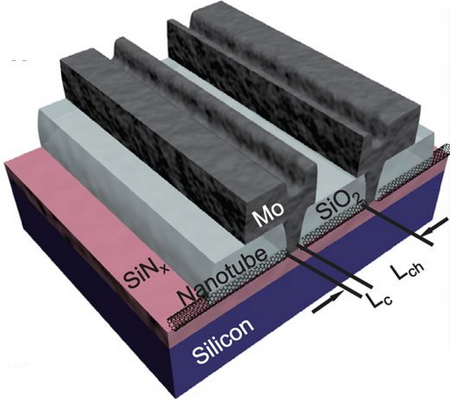
Schematic of a set of molybdenum (M0) end-contacted nanotube transistors (credit: Qing Cao et al./Science)

IBM Research has announced a “major engineering breakthrough” that could lead to carbon nanotubes replacing silicon transistors in future computing technologies.

As transistors shrink in size, electrical resistance increases within the contacts, which impedes performance. So IBM researchers invented a metallurgical process similar to microscopic welding that chemically binds the contact’s metal (molybdenum) atoms to the carbon atoms at the ends of nanotubes.

The new method promises to shrink transistor contacts without reducing performance of carbon-nanotube devices, opening a pathway to dramatically faster, smaller, and more powerful computer chips beyond the capabilities of traditional silicon semiconductors.

“This is the kind of breakthrough that we’re committed to making at IBM Research via our $3 billion investment over 5 years in research and development programs aimed a pushing the limits of chip technology,” said Dario Gil, VP, Science & Technology, IBM Research. “Our aim is to help IBM produce high-performance systems capable of handling the extreme demands of new data analytics and cognitive computing applications.”

The development was reported today in the October 2 issue of the journal Science.

Overcoming contact resistance

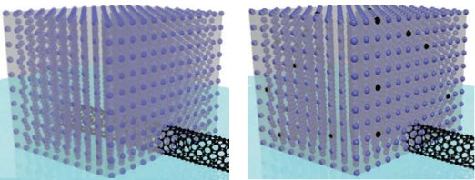
Schematic of carbon nanotube transistor contacts. Left: High-resistance side-bonded contact, where the single-wall nanotube (SWNT) (black tube) is partially covered by the metal molybdenum (Mo) (purple dots). Right: low-resistance end-bonded contact, where the SWNT is attached to the molybdenum electrode through carbide bonds, while the carbon atoms (black dots) from the originally covered portion of the SWNT uniformly diffuse out into the Mo electrode (credit: Qing Cao et al./Science)

The new “end-bonded contact scheme” allows carbon-nanotube contacts to be shrunken down to below 10 nanometers without deteriorating performance. IBM says the scheme could overcome contact resistance challenges all the way to the 1.8 nanometer node and replace silicon with carbon nanotubes.

Silicon transistors have been made smaller year after year, but they are approaching a point of physical limitation. With Moore’s Law running out of steam, shrinking the size of the transistor — including the channels and contacts — without compromising performance has been a challenge for researchers for decades.

Single wall carbon nanotube (credit: IBM)

IBM has previously shown that carbon nanotube transistors can operate as excellent switches at channel dimensions of less than ten nanometers, which is less than half the size of today’s leading silicon technology. Electrons in carbon transistors can move more easily than in silicon-based devices and use less power.

Carbon nanotubes are also flexible and transparent, making them useful for flexible and stretchable electronics or sensors embedded in wearables.

IBM acknowledges that several major manufacturing challenges still stand in the way of commercial devices based on nanotube transistors.

Earlier this summer, IBM unveiled the first 7 nanometer node silicon test chip, pushing the limits of silicon technologies.


‘Molecules’ made of light may be the basis of future computers

Researchers show that two photons, depicted in this artist’s conception as waves (left and right), can be locked together at a short distance. Under certain conditions, the photons can form a state resembling a two-atom molecule, represented as the blue dumbbell shape at center. (credit: E. Edwards/JQI)

Photons could travel side by side a specific distance from each other — similar to how two hydrogen atoms sit next to each other in a hydrogen molecule — theoretical physicists from the National Institute of Standards and Technology (NIST) and the University of Maryland (with other collaborators) have shown.

“It’s not a molecule per se, but you can imagine it as having a similar kind of structure,” says NIST’s Alexey Gorshkov. “We’re learning how to build complex states of light that, in turn, can be built into more complex objects. This is the first time anyone has shown how to bind two photons a finite distance apart.

“Lots of modern technologies are based on light, from communication technology to high-definition imaging,” Gorshkov says. “Many of them would be greatly improved if we could engineer interactions between photons.”

For example, the research could lead to new photonic computing systems, replacing slow electrons with light and reducing energy loses in the conversion from electrons to light and back.

“The detailed understanding of the [physics] also opens up an avenue towards understanding the full and much richer many-body problem involving an arbitrary number of photons in any dimension,” the authors state in a paper forthcoming in Physical Review Letters.

The findings build on previous research that several team members contributed to before joining NIST. In 2013, collaborators from Harvard, Caltech and MIT found a way to bind two photons together so that one would sit right atop the other, superimposed as they travel.


Abstract of Coulomb bound states of strongly interacting photons

We show that two photons coupled to Rydberg states via electromagnetically induced transparency can interact via an effective Coulomb potential. This interaction gives rise to a continuum of two-body bound states. Within the continuum, metastable bound states are distinguished in analogy with quasi-bound states tunneling through a potential barrier. We find multiple branches of metastable bound states whose energy spectrum is governed by the Coulomb potential, thus obtaining a photonic analogue of the hydrogen atom. Under certain conditions, the wavefunction resembles that of a diatomic molecule in which the two polaritons are separated by a finite “bond length.” These states propagate with a negative group velocity in the medium, allowing for a simple preparation and detection scheme, before they slowly decay to pairs of bound Rydberg atoms.

Intel invests US$50 million in quantum-computing research

Think of classical physics as a coin. It can be either heads or tails. If it were a bit, it would be 0 or 1. In quantum physics, this coin is best thought of as a constantly spinning coin. It represents heads and tails simultaneously. As a result, a qubit would be both 0 and 1 and spin simultaneously up and down. (credit: Intel)

Intel announced today (Thursday Sept. 3) an investment of $50 million and “significant engineering resources” in quantum computing research, in a 10-year collaborative relationship with the Delft University of Technology and TNO, the Dutch Organisation for Applied Research.

“A fully functioning quantum computer is at least a dozen years away, but the practical and theoretical research efforts we’re announcing today mark an important milestone in the journey to bring it closer to reality,” said Mike Mayberry, Intel vice president and managing director of Intel Labs.

Infographic: Quantum Computing

The Promise of Quantum Computing By Intel CEO Brian Krzanichg

Engineered bacteria form multicellular circuit to control protein expression

Two strains of synthetically engineered bacteria cooperate to create multicellular phenomena. Their fluorescence indicates the engineered capabilities have been activated. (credit: Bennett Lab/Rice University)

Rice University scientists and associates have created a biological equivalent to a computer circuit using multiple types of bacteria that change protein expression. The goal is to modify biological systems by controlling how bacteria influence each other. This could lead to bacteria that, for instance, beneficially alter the gut microbiome (collection of microorganisms) in humans.

The research is published in the journal Science.

Humans’ stomachs have a lot of different kinds of bacteria contained in the microbiome. “They naturally form a large consortium,” said Rice synthetic biologist Matthew Bennett. The idea is to engineer bacteria to be part of a consortium. “Working together allows them to effect more change than if they worked in isolation.”

In the proof-of-concept study, Bennett and his team created two strains of genetically engineered bacteria that regulate the production of proteins essential to intercellular signaling pathways, which allow cells to coordinate their efforts, generally in beneficial ways.

The synthetic microbial consortium oscillator yo-yo

The activator strain up-regulates genes in both strains; the repressor strain down-regulates genes in both strains, generating an oscillation of gene transcription in the bacterial population (credit: Ye Chen et al.)

“The main push in synthetic biology has been to engineer single cells,” Bennett said. “But now we’re moving toward multicellular systems. We want cells to coordinate their behaviors in order to elicit a populational response, just the way our bodies do.”

Bennett and his colleagues achieved their goal by engineering common Escherichia coli bacteria. By creating and mixing two genetically distinct populations, they prompted the bacteria to form a consortium.

The bacteria worked together by doing opposite tasks: One was an activator that up-regulated the expression of targeted genes; the other was a repressor that down-regulated specific genes. Together, they created oscillations of gene transcription in the bacterial population.

The two novel strains of bacteria sent out intercellular signaling molecules and created linked positive and negative feedback loops that affected gene production in the entire population. Both strains were engineered to make fluorescent reporter genes so their activities could be monitored. The bacteria were confined to microfluidic devices in the lab, where they could be monitored easily during each hours-long experiment.

When the bacteria were cultured in isolation, the protein oscillations did not appear, the researchers wrote.

Programmed yogurt, anyone?

Bennett said his lab’s work will help researchers understand how cells communicate, an important factor in fighting disease. “We have many different types of cells in our bodies, from skin cells to liver cells to pancreatic cells, and they all coordinate their behaviors to make us work properly,” he said. “To do this, they often send out small signaling molecules that are produced in one cell type and effect change in another cell type.

“We take that principle and engineer it into these very simple organisms to see if we can understand and build multicellular systems from the ground up.”

Ultimately, people might ingest the equivalent of biological computers that can be programmed through one’s diet, Bennett said. “One idea is to create a yogurt using engineered bacteria,” he said. “The patient eats it and the physician controls the bacteria through the patient’s diet. Certain combinations of molecules in your food can turn systems within the synthetic bacteria on and off, and then these systems can communicate with each other to effect change within your gut.”

KAIST and University of Houston scientists were also involved in the research. The National Institutes of Health, the Robert A. Welch Foundation, the Hamill Foundation, the National Science Foundation, and the China Scholarship Council supported the research.


Abstract of Emergent genetic oscillations in a synthetic microbial consortium

A challenge of synthetic biology is the creation of cooperative microbial systems that exhibit population-level behaviors. Such systems use cellular signaling mechanisms to regulate gene expression across multiple cell types. We describe the construction of a synthetic microbial consortium consisting of two distinct cell types—an “activator” strain and a “repressor” strain. These strains produced two orthogonal cell-signaling molecules that regulate gene expression within a synthetic circuit spanning both strains. The two strains generated emergent, population-level oscillations only when cultured together. Certain network topologies of the two-strain circuit were better at maintaining robust oscillations than others. The ability to program population-level dynamics through the genetic engineering of multiple cooperative strains points the way toward engineering complex synthetic tissues and organs with multiple cell types.

Optical chip allows for reprogramming quantum computer in seconds

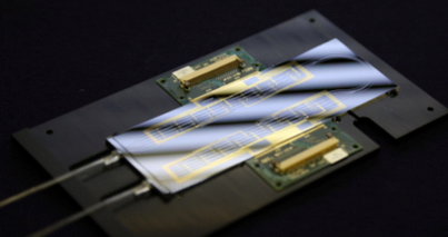
Linear optics processor (credit: University of Bristol)

A fully reprogrammable optical chip that can process photons in quantum computers in an infinite number of ways have been developed by researchers from the University of Bristol in the UK and Nippon Telegraph and Telephone (NTT) in Japan.

The universal “linear optics processor” (LPU) chip is a major step forward in creating a quantum computer to solve problems such as designing new drugs, superfast database searches, and performing otherwise intractable mathematics that aren’t possible for supercomputers — marking a new era of research for quantum scientists and engineers at the cutting edge of quantum technologies, the researchers say.

The chip solves a major barrier in testing new theories for quantum science and quantum computing: the time and resources needed to build new experiments, which are typically extremely demanding due to the notoriously fragile nature of quantum systems.

DIY photonics

“A whole field of research has essentially been put onto a single optical chip that is easily controlled,” said University of Bristol research associate Anthony Laing, PhD, project leader and senior author of a paper on the research in the journal Science today (August 14).

“The implications of the work go beyond the huge resource savings. Now anybody can run their own experiments with photons, much like they operate any other piece of software on a computer. They no longer need to convince a physicist to devote many months of their life to painstakingly build and conduct a new experiment.”

Linear optics processing system (credit: J. Carolan et al./Science)

The team demonstrated that by reprogramming it to rapidly perform a number of different experiments, each of which would previously have taken many months to build.

“Once we wrote the code for each circuit, it took seconds to reprogram the chip, and milliseconds for the chip to switch to the new experiment,” explained Bristol PhD student Jacques Carolan, one of the researchers. “We carried out a year’s worth of experiments in a matter of hours. What we’re really excited about is using these chips to discover new science that we haven’t even thought of yet.”

The University of Bristol’s pioneering Quantum in the Cloud is the first service to make a quantum processor publicly accessible. They plan to add more chips like the LPU to the service “so others can discover the quantum world for themselves.”


Abstract of Universal linear optics

Linear optics underpins fundamental tests of quantum mechanics and quantum technologies. We demonstrate a single reprogrammable optical circuit that is sufficient to implement all possible linear optical protocols up to the size of that circuit. Our six-mode universal system consists of a cascade of 15 Mach-Zehnder interferometers with 30 thermo-optic phase shifters integrated into a single photonic chip that is electrically and optically interfaced for arbitrary setting of all phase shifters, input of up to six photons, and their measurement with a 12-single-photon detector system. We programmed this system to implement heralded quantum logic and entangling gates, boson sampling with verification tests, and six-dimensional complex Hadamards. We implemented 100 Haar random unitaries with an average fidelity of 0.999 ± 0.001. Our system can be rapidly reprogrammed to implement these and any other linear optical protocol, pointing the way to applications across fundamental science and quantum technologies.

Cheap, power-efficient flash memory for big data without sacrificing speed

A 20-node BlueDBM Cluster (credit: Sang-Woo Jun et al./ISCA 2015)

There’s a big problem with big data: the huge RAM memory required. Now MIT researchers have developed a new system called “BlueDBM” that should make servers using flash memory as efficient as those using conventional RAM for several common big-data applications, while preserving their power and cost savings.

Here’s the context: Data sets in areas such as genomics, geological data, and daily twitter feeds can be as large as 5TB to 20 TB. Complex data queries in such data sets require high-speed random-access memory (RAM). But that would require a huge cluster with up to 100 servers, each with 128GB to 256GBs of DRAM (dynamic random access memory).

Flash memory (used in smart phones and other portable devices) could provide an alternative to conventional RAM for such applications. It’s about a tenth as expensive, and it consumes about a tenth as much power. The problem: it’s also a tenth as fast.

But at the International Symposium on Computer Architecture in June, the MIT researchers, with colleagues at Quanta Computer, presented experimental evidence showing that if conventional servers executing a distributed computation have to go to disk for data even 5 percent of the time, their performance falls to a level that’s comparable with flash anyway.

In fact, they found that for a 10.5-terabyte computation, just 20 servers with 20 terabytes’ worth of flash memory each could do as well as 40 servers with 10 terabytes’ worth of RAM, and could consume only a fraction as much power. This was even without the researchers’ new techniques for accelerating data retrieval from flash memory.

“This is not a replacement for DRAM [dynamic RAM] or anything like that,” says Arvind, the Johnson Professor of Computer Science and Engineering at MIT, whose group performed the new work. “But there may be many applications that can take advantage of this new style of architecture. Which companies recognize — everybody’s experimenting with different aspects of flash. We’re just trying to establish another point in the design space.”

Technical details

The researchers were able to make a network of flash-based servers competitive with a network of RAM-based servers by moving a little computational power off of the servers and onto the chips that control the flash drives. By preprocessing some of the data on the flash drives before passing it back to the servers, those chips can make distributed computation much more efficient. And since the preprocessing algorithms are wired into the chips, they dispense with the computational overhead associated with running an operating system, maintaining a file system, and the like.

With hardware contributed by some of their sponsors — Quanta, Samsung, and Xilinx — the researchers built a prototype network of 20 servers. Each server was connected to a field-programmable gate array, or FPGA, a kind of chip that can be reprogrammed to mimic different types of electrical circuits. Each FPGA, in turn, was connected to two half-terabyte — or 500-gigabyte — flash chips and to the two FPGAs nearest it in the server rack.

Because the FPGAs were connected to each other, they created a very fast network that allowed any server to retrieve data from any flash drive. They also controlled the flash drives, which is no simple task: The controllers that come with modern commercial flash drives have as many as eight different processors and a gigabyte of working memory.

Finally, the FPGAs also executed the algorithms that preprocessed the data stored on the flash drives. The researchers tested three such algorithms, geared to three popular big-data applications. One is image search, or trying to find matches for a sample image in a huge database. Another is an implementation of Google’s PageRank algorithm, which assesses the importance of different Web pages that meet the same search criteria. And the third is an application called Memcached, which big, database-driven websites use to store frequently accessed information.

FPGAs are about one-tenth as fast as purpose-built chips with hardwired circuits, but they’re much faster than central processing units using software to perform the same computations. Ordinarily, either they’re used to prototype new designs, or they’re used in niche products whose sales volumes are too small to warrant the high cost of manufacturing purpose-built chips.

But the MIT and Quanta researchers’ design suggests a new use for FPGAs: A host of applications could benefit from accelerators like the three the researchers designed. And since FPGAs are reprogrammable, they could be loaded with different accelerators, depending on the application. That could lead to distributed processing systems that lose little versatility while providing major savings in energy and cost.

“Many big-data applications require real-time or fast responses,” says Jihong Kim, a professor of computer science and engineering at Seoul National University. “For such applications, BlueDBM” — the MIT and Quanta researchers’ system — “is an appealing solution.”

Relative to some other proposals for streamlining big-data analysis, “The main advantage of BlueDBM might be that it can easily scale up to a lot bigger storage system with specialized accelerated supports,” Kim says.


Abstract of BlueDBM: An Appliance for Big Data Analytics

Complex data queries, because of their need for random accesses, have proven to be slow unless all the data can be accommodated in DRAM. There are many domains, such as genomics, geological data and daily twitter feeds where the datasets of interest are 5TB to 20 TB. For such a dataset, one would need a cluster with 100 servers, each with 128GB to 256GBs of DRAM, to accommodate all the data in DRAM. On the other hand, such datasets could be stored easily in the flash memory of a rack-sized cluster. Flash storage has much better random access performance than hard disks, which makes it desirable for analytics workloads. In this paper we present BlueDBM, a new system architecture which has flashbased storage with in-store processing capability and a low-latency high-throughput inter-controller network. We show that BlueDBM outperforms a flash-based system without these features by a factor of 10 for some important applications. While the performance of a ram-cloud system falls sharply even if only 5%~10% of the references are to the secondary storage, this sharp performance degradation is not an issue in BlueDBM. BlueDBM presents an attractive point in the cost-performance trade-off for Big Data analytics.