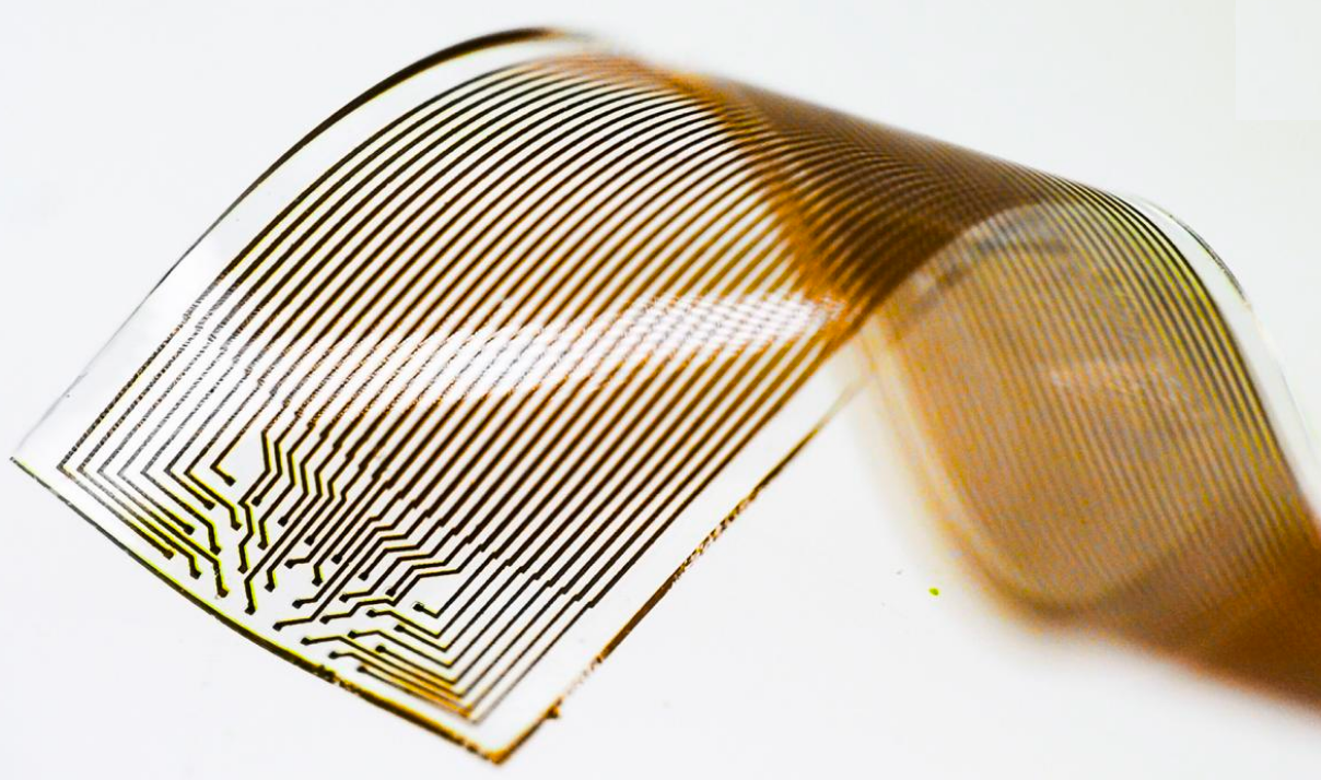
Artificial sensory neurons may give future prosthetic devices and robots a subtle sense of touch

American and Korean researchers are creating an artificial nerve system for robots and humans. (credit: Kevin Craft)

Researchers at Stanford University and Seoul National University have developed an artificial sensory nerve system that’s a step toward artificial skin for prosthetic limbs, restoring sensation to amputees, and giving robots human-like reflexes.*

Their rudimentary artificial nerve circuit integrates three previously developed components: a touch-pressure sensor, a flexible electronic neuron, and an artificial synaptic transistor modeled on human synapses.

Here’s how the artificial nerve circuit works:

(Biological model) Pressures applied to afferent (sensory) mechanoreceptors (pressure sensors, in this case) in the finger change the receptor potential (voltage) of each mechanoreceptor. The receptor potential changes combine and initiate action potentials in the nerve fiber, connected to a heminode in the chest. The nerve fiber forms synapses with interneurons in the spinal cord. Action potentials from multiple nerve fibers combine through the synapses and contribute to information processing (via postsynaptic potentials). (credit: (Yeongin Kim (Stanford University), Alex Chortos(Stanford University), Wentao Xu (Seoul National University), Zhenan Bao (Stanford University), Tae-Woo Lee (Seoul National University))

(Artificial model) Illustration of a corresponding artificial afferent nerve system made of pressure sensors, an organic ring oscillator (simulates a neuron), and a transistor that simulates a synapse. (Only one ring oscillator connected to a synaptic transistor is shown here for simplicity.) Colors of parts match corresponding colors in the biological version. (credit: Yeongin Kim (Stanford University), Alex Chortos (Stanford University), Wentao Xu (Seoul National University), Zhenan Bao (Stanford University), Tae-Woo Lee (Seoul National University))

(Photo) Artificial sensor, artificial neuron, and artificial synapse. (credit: Yeongin Kim (Stanford University), Alex Chortos(Stanford University), Wentao Xu (Seoul National University), Zhenan Bao (Stanford University), Tae-Woo Lee (Seoul National University))

Experiments with the artificial nerve circuit

In a demonstration experiment, the researchers used the artificial nerve circuit to activate the twitch reflex in the knee of a cockroach.

A cockroach insect (A) with an attached artificial mechanosensory nerve was used in this experiment. The artificial afferent nerve (B) was connected to the biological motor (movement) nerves of a detached insect leg (B, lower right) to demonstrate a hybrid reflex arc (such as a knee reflex). Applied pressure caused a reflex movement of the leg. A force gauge (C) was used to measure the force of the reflex movements of the disabled insect leg. (credit: Yeongin Kim (Stanford University), Alex Chortos(Stanford University), Wentao Xu (Seoul National University), Zhenan Bao (Stanford University), Tae-Woo Lee (Seoul National University))

The researchers did another experiment that showed how the artificial nerve system could be used to identify letters in the Braille alphabet.

Improving robot and human sensory abilites

iCub robot (credit: D. Farina/Istituto Italiano Di Tecnologia)

The researchers “used a knee reflex as an example of how more-advanced artificial nerve circuits might one day be part of an artificial skin that would give prosthetic devices or robots both senses and reflexes,” noted Chiara Bartolozzi, Ph.D., of Istituto Italiano Di Tecnologia, writing in a Science commentary on the research.

Tactile information from artificial tactile systems “can improve the interaction of a robot with objects,” says Bartolozzi, who is involved in research with the iCub robot.

“In this scenario, objects can be better recognized because touch complements the information gathered from vision about the shape of occluded or badly illuminated regions of the object, such as its texture or hardness. Tactile information also allows objects to be better manipulated — for example, by exploiting contact and slip detection to maintain a stable but gentle grasp of fragile or soft objects (see the photo). …

“Information about shape, softness, slip, and contact forces also greatly improves the usability of upper-limb prosthetics in fine manipulation. … The advantage of the technology devised by Kim et al. is the possibility of covering at a reasonable cost larger surfaces, such as fingers, palms, and the rest of the prosthetic device.

“Safety is enhanced when sensing contacts inform the wearer that the limb is encountering obstacles. The acceptability of the artificial hand by the wearer is also improved because the limb is perceived as part of the body, rather than as an external device. Lower-limb prostheses can take advantage of the same technology, which can also provide feedback about the distribution of the forces at the foot while walking.”

Next research steps

The researchers plan next to create artificial skin coverings for prosthetic devices, which will require new devices to detect heat and other sensations, the ability to embed them into flexible circuits, and then a way to interface all of this to the brain. They also hope to create low-power, artificial sensor nets to cover robots. The idea is to make them more agile by providing some of the same feedback that humans derive from their skin.

“We take skin for granted but it’s a complex sensing, signaling and decision-making system,” said Zhenan Bao, Ph.D., a Stanford professor of chemical engineering and one of the senior authors. “This artificial sensory nerve system is a step toward making skin-like sensory neural networks for all sorts of applications.”

This milestone is part of Bao’s quest to mimic how skin can stretch, repair itself, and, most remarkably, act like a smart sensory network that knows not only how to transmit pleasant sensations to the brain, but also when to order the muscles to react reflexively to make prompt decisions.

The synaptic transistor is the brainchild of Tae-Woo Lee of Seoul National University, who spent his sabbatical year in Bao’s Stanford lab to initiate the collaborative work.

Reference: Science May 31. Source: Stanford University and Seoul National University.

* This work was funded by the Ministry of Science and ICT, Korea; by Seoul National University (SNU); by Samsung Electronics; by the National Nanotechnology Coordinated Infrastructure; and by the Stanford Nano Shared Facilities (SNSF). Patents related to this work are planned.

Ingestible capsule uses light-emitting bacteria to monitor gastrointestinal health

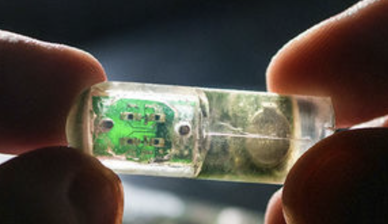
MIT-designed biosensor capsule uses genetically engineered light-emitting bacteria (right) to detect molecules that identify bleeding or other gastrointestinal problems. Ultra-low-power electronics (left) sense the light and send diagnostic information wirelessly to a cellphone. (credit: Lillie Paquette/MIT)

MIT engineers have designed and built a tiny ingestible biosensor* capsule that can diagnose gastrointestinal problems, and the engineers demonstrated its ability to detect bleeding in pigs.

Currently, if patients are suspected to be bleeding from a gastric ulcer, for example, they have to undergo an endoscopy to diagnose the problem, which often requires the patient to be sedated.

If the engineers can shrink the sensor capsule and detect a variety of other conditions, the research could potentially transform the diagnosis of gastrointestinal diseases and conditions, according to the researchers.

Diagnosing gastrointestinal diseases in real time

To detect diseases or conditions, the genetically engineered bacteria (green) are placed into multiple wells (blue), covered by a semipermeable membrane (white) that allows small molecules (red) from the surrounding environment to diffuse through. The bacteria luminesce (glow) when they sense the specific type of molecule they are designed for. (In the experiment with pigs, heme — part of the red hemoglobin blood pigment — indicated bleeding.) A phototransistor (brown) measures the amount of light produced by the bacterial cells and relays that information to a microprocessor in the capsule, which then sends a wireless signal to a nearby computer or smartphone. (credit: Mark Mimee et al./Science)

The researchers showed that the ingestible biosensor could correctly determine whether any blood was present in the pig’s stomach. They anticipate that this type of sensor could be deployed for either one-time use or to remain in the digestive tract for several days or weeks, sending continuous signals. The sensors could also be designed to carry multiple strains of bacteria, allowing for diagnosing multiple diseases and conditions.

The researchers plan to reduce the size of the sensor capsule (currently 10 millimeters wide by 30 millimeters long) and to study how long the bacteria cells can survive in the digestive tract. They also hope to develop sensors for gastrointestinal conditions other than bleeding.**

Reference: Science. Source: MIT.

* The sensor requires only 13 microwatts of power. The researchers equipped the sensor with a 2.7-volt battery, which they estimate could power the device for about 1.5 months of continuous use. They say it could also be powered by a voltaic cell sustained by acidic fluids in the stomach, using previously developed MIT technology.

** For example, one of the sensors they designed detects a sulfur-containing ion called thiosulfate, which is linked to inflammation and could be used to monitor patients with Crohn’s disease or other inflammatory conditions. Another one detects a bacterial signaling molecule called AHL, which can serve as a marker for gastrointestinal infections because different types of bacteria produce slightly different versions of the molecule.


Revolutionary 3D nanohybrid lithium-ion battery could allow for charging in just seconds [UPDATED]

Left: Conventional composite battery design, with 2D stacked anode and cathode (black and red materials). Right: New 3D nanohybrid lithium-ion battery design, with multiple anodes and cathodes nanometers apart for high-speed charging. (credit: Cornell University)

Cornell University engineers have designed a revolutionary 3D lithium-ion battery that could be charged in just seconds.

In a conventional battery, the battery’s anode and cathode* (the two sides of a battery connection) are stacked in separate columns (the black and red columns in the left illustration above). For the new design, the engineers instead used thousands of nanoscale (ultra-tiny) anodes and cathodes (shown in the illustration on the right above).

Putting those thousands of anodes and cathodes just 20 nanometers (billionths of a meter) apart dramatically extends the area, allowing for extremely fast charging** (in seconds or less) and also allows for holding more power for longer.

Left-to-right: The anode was made of self-assembling (automatically grown) thin-film carbon material with thousands of regularly spaced pores (openings), each about 40 nanometers wide. The pores were coated with a 10 nanometer-thick electrolyte* material (the blue layer between the black anode layer, as shown in the “Electrolyte coating” illustration), which is electronically insulating but conducts ions (an ion is an atom or molecule that has an electrical charge and is what flows inside a battery instead of electrons). The cathode was made from sulfur. (credit: Cornell University)

In addition, unlike traditional batteries, the electrolyte battery material does not have pinholes (tiny holes), which can lead to short-circuiting the battery, giving rise to fires in mobile devices, such as cellphones and laptops.

The engineers are still perfecting the technique, but they have applied for patent protection on the proof-of-concept work, which was funded by the U.S. Department of Energy and in part by the National Science Foundation.

Reference: Energy & Environmental Science (open source with registration) March 9, 2018. Source: Cornell University May 16, 2018.

* How batteries work

Batteries have three parts. An anode (-) and a cathode (+) — the positive and negative sides at either end of a traditional battery — which are hooked up to an electrical circuit (green); and the electrolyte, which keeps the anode and cathode apart and allows ions (electrically charged atoms or molecules) to flow. (credit: Northwestern University Qualitative Reasoning Group)


** Also described as high “power density.” In addition, “Batteries with nanostructured architectures promise improved power output, as close proximity of the two electrodes is beneficial for fast ion diffusion, while high material loading simultaneously enables high energy density” (hold more power for longer). — J. G. Werner et al./Energy Environ. Sci.

UPDATED May 21, 2018 to include explanations of technical terms

Three dramatic new ways to visualize brain tissue and neuron circuits

Visualizing the brain: Here, tissue from a human dentate gyrus (a part of the brain’s hippocampus that is involved in the formation of new memories) was imaged transparently in 3D and colored-coded to reveal the distribution and types of nerve cells. (credit: The University of Hong Kong)

Visualizing human brain tissue in vibrant transparent colors

Neuroscientists from The University of Hong Kong (HKU) and Imperial College London have developed a new method called “OPTIClear” for 3D transparent color visualization (at the microscopic level) of complex human brain circuits.

To understand how the brain works, neuroscientists map how neurons (nerve cells) are wired to form circuits in both healthy and disease states. To do that, the scientists typically cut brain tissues into thin slices. Then they trace the entangled fibers across those slices — a complex, laborious process.

Making human tissues transparent. OPTIClear replaces that process by “clearing” (making tissues transparent) and using fluorescent staining to identify different types of neurons. In one study of more than 3,000 large neurons in the human basal forebrain, the researchers were able to reduce the time from about three weeks to five days to visualize neurons, glial cells, and blood vessels in exquisite 3D detail. Previous clearing methods (such as CLARITY) have been limited to rodent tissue.

Reference (open access): Nature Communications March 14, 2018. Source: HKU and Imperial College London, May 7, 2018

Watching millions of brain cells in a moving animal for the first time

Neurons in the hippocampus flash on and off as a mouse walks around with tiny camera lenses on its head. (credit: The Rockefeller University)

It’s a neuroscientist’s dream: being able to track the millions of interactions among brain cells in animals that move about freely — allowing for studying brain disorders. Now a new invention, developed at The Rockefeller University and reported today, is expected to give researchers a dynamic tool to do that just that, eventually in humans.

The new tool can track neurons located at different depths within a volume of brain tissue in a freely moving rodent, or record the interplay among neurons when two animals meet and interact socially.

Microlens array for 3D recording. The technology consists of a tiny microscope attached to a mouse’s head, with a group of lenses called a “microlens array.” These lenses enable the microscope to capture images from multiple angles and depths on a sensor chip, producing a three-dimensional record of neurons blinking on and off as they communicate with each other through electrochemical impulses. (The mouse neurons are genetically modified to light up when they become activated.) A cable attached to the top of the microscope transmits the data for recording.

One challenge: Brain tissue is opaque, making light scatter, which makes it difficult to pinpoint the source of each neuronal light flash. The researchers’ solution: a new computer algorithm (program), known as SID, that extracts additional information from the scattered emission light.

Reference: Nature Methods. Source: The Rockefeller University May 7, 2018

Brain cells interacting in real time

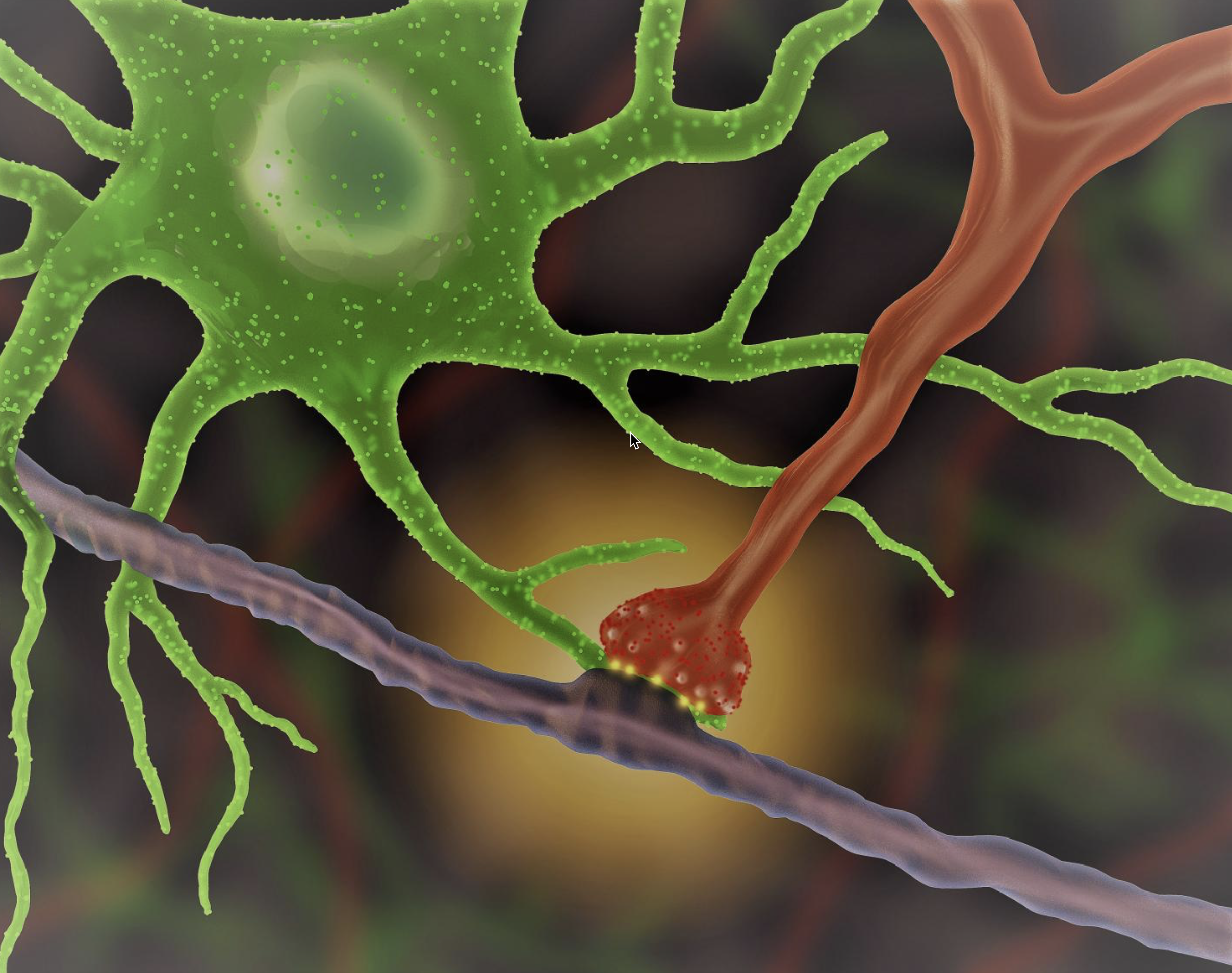
Illustration: An astrocyte (green) interacts with a synapse (red), producing an optical signal (yellow). (credit: UCLA/Khakh lab)

Researchers at the David Geffen School of Medicine at UCLA can now peer deep inside a mouse’s brain to watch how star-shaped astrocytes (support glial cells in the brain) interact with synapses (the junctions between neurons) to signal each other and convey messages.

The method uses different colors of light that pass through a lens to magnify objects that are invisible to the naked eye. The viewable objects are now far smaller than those viewable by earlier techniques. That enables researchers to observe how brain damage alters the way astrocytes interact with neurons, and develop strategies to address these changes, for example.

Astrocytes are believed to play a key role in neurological disorders like Lou Gehrig’s, Alzheimer’s, and Huntington’s disease.

Reference: Neuron. Source: UCLA Khakh lab April 4, 2018.

round-up | Hawking’s radical instant-universe-as-hologram theory and the scary future of information warfare

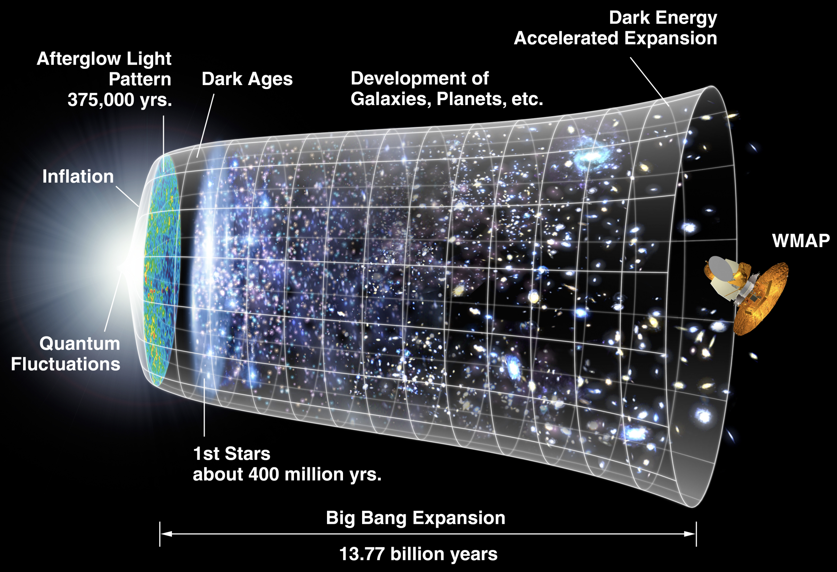
A timeline of the Universe based on the cosmic inflation theory (credit: WMAP science team/NASA)

Stephen Hawking’s final cosmology theory says the universe was created instantly (no inflation, no singularity) and it’s a hologram

There was no singularity just after the big bang (and thus, no eternal inflation) — the universe was created instantly. And there were only three dimensions. So there’s only one finite universe, not a fractal or a multiverse — and we’re living in a projected hologram. That’s what Hawking and co-author Thomas Hertog (a theoretical physicist at the Catholic University of Leuven) have concluded — contradicting Hawking’s former big-bang singularity theory (with time as a dimension).

Problem: So how does time finally emerge? “There’s a lot of work to be done,” admits Hertog. Citation (open access): Journal of High Energy Physics, May 2, 2018. Source (open access): Science, May 2, 2018


Movies capture the dynamics of an RNA molecule from the HIV-1 virus. (photo credit: Yu Xu et al.)

Molecular movies of RNA guide drug discovery — a new paradigm for drug discovery

Duke University scientists have invented a technique that combines nuclear magnetic resonance imaging and computationally generated movies to capture the rapidly changing states of an RNA molecule.

It could lead to new drug targets and allow for screening millions of potential drug candidates. So far, the technique has predicted 78 compounds (and their preferred molecular shapes) with anti-HIV activity, out of 100,000 candidate compounds. Citation: Nature Structural and Molecular Biology, May 4, 2018. Source: Duke University, May 4, 2018.


Chromium tri-iodide magnetic layers between graphene conductors. By using four layers, the storage density could be multiplied. (credit: Tiancheng Song)

Atomically thin magnetic memory

University of Washington scientists have developed the first 2D (in a flat plane) atomically thin magnetic memory — encoding information using magnets that are just a few layers of atoms in thickness — a miniaturized, high-efficiency alternative to current disk-drive materials.

In an experiment, the researchers sandwiched two atomic layers of chromium tri-iodide (CrI3) — acting as memory bits — between graphene contacts and measured the on/off electron flow through the atomic layers.

The U.S. Dept. of Energy-funded research could dramatically increase future data-storage density while reducing energy consumption by orders of magnitude. Citation: Science, May 3, 2018. Source: University of Washington, May 3, 2018.


Definitions of artificial intelligence (credit: House of Lords Select Committee on Artificial Intelligence)

A Magna Carta for the AI age

A report by the House of Lords Select Committee on Artificial Intelligence in the U.K. lays out “an overall charter for AI that can frame practical interventions by governments and other public agencies.”

The key elements: Be developed for the common good. Operate on principles of intelligibility and fairness: users must be able to easily understand the terms under which their personal data will be used. Respect rights to privacy. Be grounded in far-reaching changes to education. Teaching needs reform to utilize digital resources, and students must learn not only digital skills but also how to develop a critical perspective online. Never be given the autonomous power to hurt, destroy or deceive human beings.

Source: The Washington Post, May 2, 2018.


(credit: CB Insights)

The future of information warfare

Memes and social networks have become weaponized, but many governments seem ill-equipped to understand the new reality of information warfare.

The weapons include: Computational propaganda: digitizing the manipulation of public opinion; advanced digital deception technologies; malicious AI impersonating and manipulating people; and AI-generated fake video and audio. Counter-weapons include: Spotting AI-generated people; uncovering hidden metadata to authenticate images and videos; blockchain for tracing digital content back to the source; and detecting image and video manipulation at scale.

Source (open-access): CB Insights Research Brief, May 3, 2018.

round-up | Three radical new user interfaces

Holodeck-style holograms could revolutionize videoconferencing

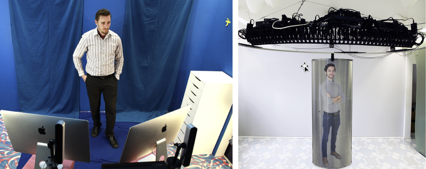
A “truly holographic” videoconferencing system has been developed by researchers at Queen’s University in Kingston Montreal. With TeleHuman 2, objects appear as stereoscopic images, as if inside a pod (not a two-dimensional video projected on a flat piece of glass). Multiple users can walk around and view the objects from all sides simultaneously — as in Star Trek’s Holodeck.

Teleporting for distance meetings. TeleHuman 2 “teleports” people live — allowing for meetings at a distance. No headset or 3D glasses required.

The researchers presented the system in an open-access paper at CHI 2018, the ACM CHI Conference on Human Factors in Computing Systems in Montreal on April 25.

(Left) Remote capture room with stereo 2K cameras, multiple surround microphones, and displays. (Right) Telehuman 2 display and projector (credit: Human Media Lab)


Interactive smart wall acts as giant touch screen, senses electromagnetic activity in room

Researchers at Carnegie Mellon University and Disney Research have devised a system called Wall++ for creating interactive “smart walls” that sense human touch, gestures, and signals from appliances.

By using masking tape and nickel-based conductive paint, a user would create a pattern of capacitive-sensing electrodes on the wall of a room (or a building) and then paint it over. The electrodes would be connected to sensors.

Wall ++ (credit: Carnegie Mellon University)

Acting as a sort of huge tablet, touch-tracking or motion-sensing uses could include dimming or turning lights on/off, controlling speaker volume, acting as smart thermostats, playing full-body video games, or creating a huge digital white board, for example.

A passive electromagnetic sensing mode could also allow for detecting devices that are on or off (by noise signature). And a small, signal-emitting wristband could enable user localization and identification for collaborative gaming or teaching, for example.

The researchers also presented an open-access paper at CHI 2018.


A smart-watch screen on your skin

LumiWatch, another interactive interface out of Carnegie Mellon, projects a smart-watch touch screen onto your skin. It solves the tiny-interface bottleneck with smart watches — providing more than five times the interactive surface area for common touchscreen operations, such as tapping and swiping. It was also presented in an open-access paper at CHI 2018.

A future ultraminiature computer the size of a pinhead?

Thin-film MRAM surface structure comprising one-monolayer iron (Fe) deposited on a boron, gallium, aluminum, or indium nitride substrate. (credit: Jie-Xiang Yu and Jiadong Zang/Science Advances)

University of New Hampshire researchers have discovered a combination of materials that they say would allow for smaller, safer magnetic random access memory (MRAM) storage — ultimately leading to ultraminiature computers.

Unlike conventional RAM (read-only memory) SRAM and DRAM chip technologies, with MRAM, data is stored by magnetic storage elements, instead of energy-expending electric charge or current flows. MRAM is also nonvolatile memory (the data is preserved when the power if turned off). The elements are formed from two ferromagnetic plates, each of which can hold a magnetization, separated by a thin insulating layer.

In their study, published March 30, 2018 in the open-access journal Science Advances, the researchers describe a new design* comprising ultrathin films, known as Fe (iron) monolayers, grown on a substrate made up of non-magnetic substances —  boron, gallium, aluminum, or indium nitride.

Ultrahigh storage density

The new design has an estimated 10-year data retention at room temperature. It can “ultimately lead to nanomagnetism and promote revolutionary ultrahigh storage density in the future,” said Jiadong Zang, an assistant professor of physics and senior author. “It opens the door to possibilities for much smaller computers for everything from basic data storage to traveling on space missions. Imagine launching a rocket with a computer the size of a pin head — it not only saves space but also a lot of fuel.”

MRAM is already challenging flash memory in a number of applications where persistent or nonvolatile memory (such as flash) is currently being used, and it’s also taking on RAM chips “in applications such as AI, IoT, 5G, and data centers,” according to a recent article in Electronic Design.**

* A provisional patent pending has been filed by UNHInnovation. This work was supported by the U.S. Department of Energy, Office of Science, Basic Energy Sciences.

** More broadly, MRAM applications are in consumer electronics, robotics, automotive , enterprise storage, and aerospace & defense, according to a market analysis and 2018–2023 forecast by Market Desk.


Abstract of Giant perpendicular magnetic anisotropy in Fe/III-V nitride thin films

Large perpendicular magnetic anisotropy (PMA) in transition metal thin films provides a pathway for enabling the intriguing physics of nanomagnetism and developing broad spintronics applications. After decades of searches for promising materials, the energy scale of PMA of transition metal thin films, unfortunately, remains only about 1 meV. This limitation has become a major bottleneck in the development of ultradense storage and memory devices. We discovered unprecedented PMA in Fe thin-film growth on the Embedded Image N-terminated surface of III-V nitrides from first-principles calculations. PMA ranges from 24.1 meV/u.c. in Fe/BN to 53.7 meV/u.c. in Fe/InN. Symmetry-protected degeneracy between x2y2 and xy orbitals and its lift by the spin-orbit coupling play a dominant role. As a consequence, PMA in Fe/III-V nitride thin films is dominated by first-order perturbation of the spin-orbit coupling, instead of second-order in conventional transition metal/oxide thin films. This game-changing scenario would also open a new field of magnetism on transition metal/nitride interfaces.


Are you ready for atom-thin, ‘invisible’ displays everywhere?

Photograph of a proof-of-concept transparent display (left), and closeups showing the display in off and on states (credit: UC Berkeley)

Bloomberg reported this morning (April 4) that Apple is planning a new iPhone with touchless gesture control and displays that curve inward gradually from top to bottom. Apple’s probable use of microLED technology promises to offer “power savings and a reduced screen thickness when put beside current-generation display panels,”according to Apple Insider.

But UC Berkeley engineers have an even more radical concept for future electronics: invisible displays, using a new atomically thin display technology.

Imagine seeing the person you’re talking to projected onto a blank wall by just pointing at it, or seeing a map pop up on your car window (ideally, matched to the road you’re on) at night and disappear when you wave it off.

Schematic of transient-electroluminescent device. An AC voltage is applied between the gate (bottom) and source (top) electrodes. Light emission occurs near the source contact edge during the moment when the AC signal switches its polarity from positive to negative (and vice versa), so both positive and negative charges are present at the same time in the semiconductor, creating light. (credit: Der-Hsien Lien et al./Nature Communications)

The secret: an ultrathin monolayer semiconductor just three atoms thick — a bright “transient electroluminescent” device that is fully transparent when turned off and that can conform to curved surfaces, even human skin.* The four different monolayer materials each emit different colors of light.

The display is currently a proof-of-concept design — just a few millimeters wide, and about 1 percent efficient (commercial LEDs have efficiencies of around 25 to 30 percent). “A lot of work remains to be done and a number of challenges need to be overcome to further advance the technology for practical applications,” explained Ali Javey, Ph.D., professor of Electrical Engineering and Computer Sciences at Berkeley.

The research study was published March 26 in an open-access paper in Nature Communications. It was funded by the National Science Foundation and the Department of Energy.

* Typically, two contact points are used in a semiconductor-based light emitting device: one for injecting negatively charged particles and one injecting positively charged particles. Making contacts that can efficiently inject these charges is a fundamental challenge for LEDs, and it is particularly challenging for monolayer semiconductors since there is so little material to work with. The Berkeley research team engineered a way around this: designing a new device that only requires one contact on the transition-metal dichalcogenide (MoS2, WS2, MoSe2, and WSe2) monolayer instead of two contacts.


Abstract of Large-area and bright pulsed electroluminescence in monolayer semiconductors

Transition-metal dichalcogenide monolayers have naturally terminated surfaces and can exhibit a near-unity photoluminescence quantum yield in the presence of suitable defect passivation. To date, steady-state monolayer light-emitting devices suffer from Schottky contacts or require complex heterostructures. We demonstrate a transient-mode electroluminescent device based on transition-metal dichalcogenide monolayers (MoS2, WS2, MoSe2, and WSe2) to overcome these problems. Electroluminescence from this dopant-free two-terminal device is obtained by applying an AC voltage between the gate and the semiconductor. Notably, the electroluminescence intensity is weakly dependent on the Schottky barrier height or polarity of the contact. We fabricate a monolayer seven-segment display and achieve the first transparent and bright millimeter-scale light-emitting monolayer semiconductor device.

Next-gen optical disc has 10TB capacity and six-century lifespan

(credit: Getty)

Scientists from RMIT University in Australia and Wuhan Institute of Technology in China have developed a radical new high-capacity optical disc called “nano-optical long-data memory” that they say can record and store 10 TB (terabytes, or trillions of bytes) of data per disc securely for more than 600 years. That’s a four-times increase of storage density and 300 times increase in data lifespan over current storage technology.

Preparing  for zettabytes of data in 2025

Forecast of exponential growth of creation of Long Data, with three-year doubling time (credit: IDC)

According to IDC’s Data Age 2025 study in 2017, the recent explosion of Big Data and global cloud storage generates 2.5 PB (1015 bytes) a day, stored in massive, power-hungry data centers that use 3 percent of the world’s electricity supply. The data centers rely on hard disks, which have limited capacity (2TB per disk) and last only two years. IDC forecasts that by 2025, the global datasphere will grow exponentially to 163 zettabytes (that’s 163 trillion gigabytes) — ten times the 16.1ZB of data generated in 2016.

Examples of massive Long Data:

  • The Square Kilometer Array (SKA) radio telescope produces 576 petabytes of raw data per hour.
  • The Brain Research through Advancing Innovative Neurotechnologies (BRAIN) Initiative to map the human brain is handling data measured in yottabytes (one trillion terabytes).
  • Studying the mutation of just one human family tree over ten generations (500 years) will require 8 terabytes of data.

IDC estimates that by 2025, nearly 20% of the data in the global datasphere will be critical to our daily lives (such as biomedical data) and nearly 10% of that will be hypercritical. “By 2025, an average connected person anywhere in the world will interact with connected devices nearly 4,800 times per day — basically one interaction every 18 seconds,” the study estimates.

Replacing hard drives with optical discs

There’s a current shift from focus on “Big Data” to “Long Data,” which enables new insights to be discovered by mining massive datasets that capture changes in the real world over decades and centuries.* The researchers say their new Long-data memory technology could offer a more cost-efficient and sustainable solution to the global data storage problem.

The new technology could radically improve the energy efficiency of data centers. It would use 1000 times less power than a hard-disk-based data center by requiring far less cooling and doing away with the energy-intensive task of data migration (backing up to a new disk) every two years. Optical discs are also inherently more secure than hard disks.

“While optical technology can expand capacity, the most advanced optical discs developed so far have only 50-year lifespans,” explained lead investigator Min Gu, a professor at RMIT and senior author of an open-access paper published in Nature Communications. “Our technique can create an optical disc with the largest capacity of any optical technology developed to date and our tests have shown it will last over half a millennium and is suitable for mass production of optical discs.”

There’s an existing Blu-ray disc technology called M-DISC, that can store data for 1,000 years, but is limited to 100 GB, compared to 6000 10 TB— 100 times more data on a disc.

“This work can be the building blocks for the future of optical long-data centers over centuries, unlocking the potential of the understanding of the long processes in astronomy, geology, biology, and history,” the researchers note in the paper. “It also opens new opportunities for high-reliability optical data memory that could survive in extreme conditions, such as high temperature and high pressure.”

How the nano-optical long-data memory technology works

The high-capacity optical data memory uses gold nanoplasmonic hybrid glass composites to encode and preserve long data over centuries. (credit: Qiming Zhang et al./Nature Communications, adapted by KurzweilAI)

The new nano-optical long-data memory technology is based on a novel gold nanoplasmonic* hybrid glass matrix, unlike the materials used in current optical discs. The technique relies on a sol-gel process, which uses chemical precursors to produce ceramics and glass with higher purity and homogeneity than conventional processes. Glass is a highly durable material that can last up to 1000 years and can be used to hold data, but has limited native storage capacity because of its inflexibility. So the team combined glass with an organic material, halving its lifespan (to 600 years) but radically increasing its capacity.

Data is further encoded by heating gold nanorods, causing them to morph, in four discrete steps, into spheres. (credit: Qiming Zhang et al./Nature Communications, adapted by KurzweilAI)

To create the nanoplasmonic hybrid glass matrix, gold nanorods were incorporated into a hybrid glass composite. The researchers chose gold because like glass, it is robust and highly durable. The system allows data to be recorded in five dimensions — three dimensions in space (data is stored in gold nanorods at multiple levels in the disc and in four different shapes), plasmonic-controlled multi-color encoding**, and light-polarization encoding.

Scientists at Monash University were also involved in the research.

* “Long Data” refers here to Big Data across millennia (both historical and future), as explained here, not to be confused with the “long data” software data type. A short history of Big Data forecasts is here.

** As explained here, here, and here.

UPDATE MAR. 27, 2018 — nano-optical long-data memory disc capacity of 600TB corrected to read 10TB.


Abstract of High-capacity optical long data memory based on enhanced Young’s modulus in nanoplasmonic hybrid glass composites

Emerging as an inevitable outcome of the big data era, long data are the massive amount of data that captures changes in the real world over a long period of time. In this context, recording and reading the data of a few terabytes in a single storage device repeatedly with a century-long unchanged baseline is in high demand. Here, we demonstrate the concept of optical long data memory with nanoplasmonic hybrid glass composites. Through the sintering-free incorporation of nanorods into the earth abundant hybrid glass composite, Young’s modulus is enhanced by one to two orders of magnitude. This discovery, enabling reshaping control of plasmonic nanoparticles of multiple-length allows for continuous multi-level recording and reading with a capacity over 10 terabytes with no appreciable change of the baseline over 600 years, which opens new opportunities for long data memory that affects the past and future.

Recording data from one million neurons in real time

(credit: Getty)

Neuroscientists at the Neuronano Research Centre at Lund University in Sweden have developed and tested an ambitious new design for processing and storing the massive amounts of data expected from future implantable brain machine interfaces (BMIs) and brain-computer interfaces (BCIs).

The system would simultaneously acquire data from more than 1 million neurons in real time. It would convert the spike data (using bit encoding) and send it via an effective communication format for processing and storage on conventional computer systems. It would also provide feedback to a subject in under 25 milliseconds — stimulating up to 100,000 neurons.

Monitoring large areas of the brain in real time. Applications of this new design include basic research, clinical diagnosis, and treatment. It would be especially useful for future implantable, bidirectional BMIs and BCIs, which are used to communicate complex data between neurons and computers. This would include monitoring large areas of the brain in paralyzed patients, revealing an imminent epileptic seizure, and providing real-time feedback control to robotic arms used by quadriplegics and others.

The system is intended for recording neural signals from implanted electrodes, such as this 32-electrode grid, used for long-term, stable neural recording and treatment of neurological disorders. (credit: Thor Balkhed)

“A considerable benefit of this architecture and data format is that it doesn’t require further translation, as the brain’s [spiking] signals are translated directly into bitcode,” making it available for computer processing and dramatically increasing the processing speed and database storage capacity.

“This means a considerable advantage in all communication between the brain and computers, not the least regarding clinical applications,” says Bengt Ljungquist, lead author of the study and doctoral student at Lund University.

Future BMI/BCI systems. Current neural-data acquisition systems are typically limited to 512 or 1024 channels and the data is not easily converted into a form that can be processed and stored on PCs and other computer systems.

“The demands on hardware and software used in the context of BMI/BCI are already high, as recent studies have used recordings of up to 1792 channels for a single subject,” the researchers note in an open-access paper published in the journal Neuroinformatics.

That’s expected to increase. In 2016, DARPA (U.S. Defense Advanced Research Project Agency) announced its Neural Engineering System Design (NESD) program*, intended “to develop an implantable neural interface able to provide unprecedented signal resolution and data-transfer bandwidth between the human brain and the digital world. …

“Neural interfaces currently approved for human use squeeze a tremendous amount of information through just 100 channels, with each channel aggregating signals from tens of thousands of neurons at a time. The result is noisy and imprecise. In contrast, the NESD program aims to develop systems that can communicate clearly and individually with any of up to one million neurons in a given region of the brain.”

System architecture overview of storage for large amounts of real time neural data, proposed by Lund University researchers. A master clock pulse (a) synchronizes n acquisition systems (b), which handles bandpass filtering, spike sorting (for spike data), and down-sampling (for narrow band data), receiving electro-physiological data from subject (e). Neuronal spike data is encoded in a data grid of neurons time bins. (c). The resulting data grid is serialized and sent over to spike data storage in HDF5 file format (d), as well as to narrow band (f) and waveform data storage (g). In this work, a and b are simulated, c and d are implemented, while f and g are suggested (not yet
implemented) components. (credit: Bengt Ljungquis et al./Neuroinformatics)

* DARPA has since announced that it has “awarded contracts to five research organizations and one company that will support the Neural Engineering System Design (NESD) program: Brown University; Columbia University; Fondation Voir et Entendre (The Seeing and Hearing Foundation); John B. Pierce Laboratory; Paradromics, Inc.; and the University of California, Berkeley. These organizations have formed teams to develop the fundamental research and component technologies required to pursue the NESD vision of a high-resolution neural interface and integrate them to create and demonstrate working systems able to support potential future therapies for sensory restoration. Four of the teams will focus on vision and two will focus on aspects of hearing and speech.”


Abstract of A Bit-Encoding Based New Data Structure for Time and Memory Efficient Handling of Spike Times in an Electrophysiological Setup.

Recent neuroscientific and technical developments of brain machine interfaces have put increasing demands on neuroinformatic databases and data handling software, especially when managing data in real time from large numbers of neurons. Extrapolating these developments we here set out to construct a scalable software architecture that would enable near-future massive parallel recording, organization and analysis of neurophysiological data on a standard computer. To this end we combined, for the first time in the present context, bit-encoding of spike data with a specific communication format for real time transfer and storage of neuronal data, synchronized by a common time base across all unit sources. We demonstrate that our architecture can simultaneously handle data from more than one million neurons and provide, in real time (< 25 ms), feedback based on analysis of previously recorded data. In addition to managing recordings from very large numbers of neurons in real time, it also has the capacity to handle the extensive periods of recording time necessary in certain scientific and clinical applications. Furthermore, the bit-encoding proposed has the additional advantage of allowing an extremely fast analysis of spatiotemporal spike patterns in a large number of neurons. Thus, we conclude that this architecture is well suited to support current and near-future Brain Machine Interface requirements.