Battery breakthrough charges in seconds, lasts for a week

Illustration representing the novel design of a hybrid supercapacitor, showing bundles of nanowires (blue) coated with 2D energy-storage materials (yellow) (credit: University of Central Florida)

University of Central Florida researchers have developed a radical new supercapacitor design that could one day replace lithium-ion batteries, allowing users to charge a mobile phone in a few seconds and with a charge that lasts a week, according to the researchers. The new battery would be flexible and a fraction of the size of a lithium-ion battery.

The proof-of-concept design is based on a hybrid supercapacitor composed of a core with millions of highly conductive nanowires coated with shells of two-dimensional materials.* It combines fast charging and discharging (high power density) and high storage capacity (high energy density).

Supercapacitor design: an array of electrically conductive nanowires (orange) with metal current-collector covering (blue) (credit: Nitin Choudhary et al./ACS Nano)

Optical image of core/shell nanowires on a tungsten foil under mechanical bending (left). Corresponding SEM image (right) shows high-density, well-aligned nanowires along with their faceted surface (inset). The scale bar in the inset is 500 nm. (credit: Nitin Choudhary et al./ACS Nano)

Another advantage would be “cyclic stability” (how many times a battery can be charged, drained and recharged before beginning to degrade). A lithium-ion battery can be recharged fewer than 1,500 times without significant failure, compared to recently developed supercapacitors based on two-dimensional materials, which can be recharged more than 30,000 times.

Supercapacitor prototype showing flexible design (credit: (credit: University of Central Florida)

Electric vehicles could also benefit from longer-range operation and sudden bursts of power and speed. The flexible material could mean a significant advancement in wearable tech, according to the researchers, and would also avoid the risk of overheating and explosion with lithium-ion batteries.

Hee-Suk Chung of Korea Basic Science Institute was also involved in the research, which was published recently in the journal ACS Nano.

* The core nanowire material is tungsten trioxide (WO3) and the two-dimensional shell material is a transition-metal dichalcogenide, tungsten disulfide (WS2).

Ragone plot to compare the performances of various technologies with the core/shell nanowires supercapacitor in this study (credit: Nitin Choudhary et al./ACS Nano)

Galvanostatic Charging/Discharging (GCD) various current densities in the voltage range of 0.3 and 0.5 V, showing nearly symmetrical voltage curves, indicating highly reversible and fast responses. (credit: Nitin Choudhary et al./ACS Nano)


Abstract of High-Performance One-Body Core/Shell Nanowire Supercapacitor Enabled by Conformal Growth of Capacitive 2D WS2 Layers

Two-dimensional (2D) transition-metal dichalcogenides (TMDs) have emerged as promising capacitive materials for supercapacitor devices owing to their intrinsically layered structure and large surface areas. Hierarchically integrating 2D TMDs with other functional nanomaterials has recently been pursued to improve electrochemical performances; however, it often suffers from limited cyclic stabilities and capacitance losses due to the poor structural integrity at the interfaces of randomly assembled materials. Here, we report high-performance core/shell nanowire supercapacitors based on an array of one-dimensional (1D) nanowires seamlessly integrated with conformal 2D TMD layers. The 1D and 2D supercapacitor components possess “one-body” geometry with atomically sharp and structurally robust core/shell interfaces, as they were spontaneously converted from identical metal current collectors via sequential oxidation/sulfurization. These hybrid supercapacitors outperform previously developed any stand-alone 2D TMD-based supercapacitors; particularly, exhibiting an exceptional charge–discharge retention over 30,000 cycles owing to their structural robustness, suggesting great potential for unconventional energy storage technologies.

This tiny electronic device applied to the skin can pick up heart and speech sounds

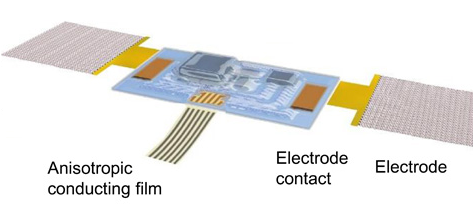
Illustration of the assembled acoustic sensor device and its interface with soft electrophysiology measurement electrodes and flexible cable for power supply and data acquisition (credit: Yuhao Liu et al./Science Advances)

Researchers from the University of Colorado Boulder and Northwestern University have developed a tiny, soft, wearable acoustic sensor that measures vibrations in the human body and can be used to monitor human heart health and recognize spoken words.

The stretchable Band-aid-like device attaches to the skin on nearly any surface of the body, using “epidermal electronics” to capture sound signals from the body.

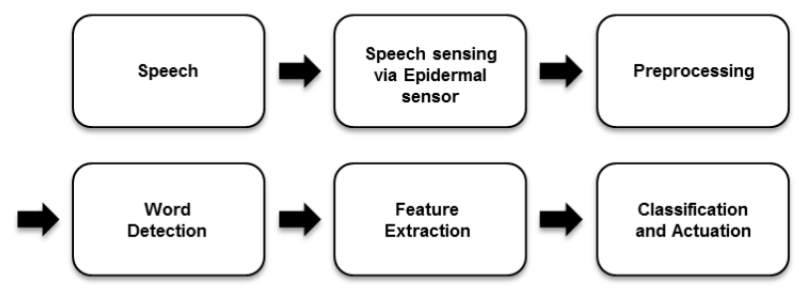
It’s a sort of tiny, wearable stethoscope. As described in an open-access paper published Nov. 16 in Science Advances, a sister journal of Science, it can detect things like heart murmurs in cardiac patients and lung problems, and can monitor ventricular assist devices. It can also be used to pick up speech sounds (for automated speech recognition or controlling video games and other machines), and even movements in gastrointestinal tracts.

Listening in on the body

The sensor can also integrate electrodes that can record electrocardiogram (ECG) signals that measure the electrical activity of the heart as well electromyogram (EMG) signals that measure the electrical activity of muscles at rest and during contraction.

While the sensor was wired to an external data acquisition system for the tests, it can easily be converted into a wireless device, said CU Boulder Assistant Professor Jae-Woong Jeong, a lead author. Such sensors could be of use in remote, noisy places — including battlefields — producing quiet, high-quality cardiology or speech signals that can be read in real time at distant medical facilities.

Using the data from these sensors, a doctor at a hospital far away from a patient would be able to make a fast, accurate diagnosis, said Jeong.

Process loop for a speech-based human-machine interface (credit: Yuhao Liu et al./Science Advances)

Vocal cord vibration signals also could be used by the military personnel or civilians to control robots, vehicles or drones. The speech recognition capabilities of the sensor also have implications for improving communication for people suffering from speech impairments, he said.

As part of the study, the team used the device to measure cardiac acoustic responses and ECG activity — including the detection of heart murmurs — in a group of elderly volunteers.

The researchers also were able to detect the acoustical signals of blood clots in a related lab experiment, said Jeong.


University of Colorado Boulder | CU Science Story — Wearable Tech


Abstract of Epidermal mechano-acoustic sensing electronics for cardiovascular diagnostics and human-machine interfaces

Physiological mechano-acoustic signals, often with frequencies and intensities that are beyond those associated with the audible range, provide information of great clinical utility. Stethoscopes and digital accelerometers in conventional packages can capture some relevant data, but neither is suitable for use in a continuous, wearable mode, and both have shortcomings associated with mechanical transduction of signals through the skin. We report a soft, conformal class of device configured specifically for mechano-acoustic recording from the skin, capable of being used on nearly any part of the body, in forms that maximize detectable signals and allow for multimodal operation, such as electrophysiological recording. Experimental and computational studies highlight the key roles of low effective modulus and low areal mass density for effective operation in this type of measurement mode on the skin. Demonstrations involving seismocardiography and heart murmur detection in a series of cardiac patients illustrate utility in advanced clinical diagnostics. Monitoring of pump thrombosis in ventricular assist devices provides an example in characterization of mechanical implants. Speech recognition and human-machine interfaces represent additional demonstrated applications. These and other possibilities suggest broad-ranging uses for soft, skin-integrated digital technologies that can capture human body acoustics.

Semiconductor-free microelectronics using metamaterials: faster, can handle more power

Illustration of semiconductor-free microelectronic device (credit: UC San Diego Applied Electromagnetics Group)

University of California San Diego engineers have made the first semiconductor-free, optically controlled microelectronic device, using metamaterials, with a 1,000 % increase in conductivity when activated by low voltage and a low-power laser.

The discovery may lead to microelectronic devices that are faster and capable of handling more power, and to more efficient solar panels. The work was published Nov. 4 in Nature Communications (open access).

Replacing semiconductors with free electrons in space, similar to how vacuum tubes work (credit: UC San Diego Applied Electromagnetics Group)

Semiconductors impose limits on a device’s conductivity, or electron flow, since electrons are constantly colliding with atoms as they flow through the semiconductor. To remove these roadblocks to conductivity, the engineers replaced semiconductors with free electrons in space, similar to how vacuum tubes work.

However, liberating electrons from materials is challenging. It requires either applying high voltages (at least 100 volts for cold-cathode emitters), or high power lasers, or extremely high temperatures (more than 1,000 degrees Fahrenheit for thermionic emission) — all impractical in making micro- and nanoscale electronic devices.

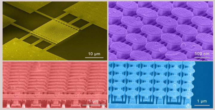
Scanning electron micrograph images showing the semiconductor-free microelectronic device (top left) and details of the gold metasurface (top right, bottom). (credit: UC San Diego Applied Electromagnetics Group)

To address this challenge, Sievenpiper’s team fabricated a microscale device that can release electrons from a material without such extreme requirements. The device consists of an engineered surface, called a “metasurface,” on top of a silicon wafer, with a layer of silicon dioxide in between. The metasurface consists of an array of gold mushroom-like nanostructures on an array of parallel gold strips.*

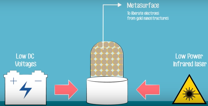
The gold metasurface is designed such that when a low DC voltage (under 10 volts) and a compact, low-power infrared laser are both applied, the metasurface generates “hot spots” — areas with a high-intensity electric field — that provide enough energy to pull electrons out from the metal and liberate them into space. (credit: UC San Diego Applied Electromagnetics Group)

Best for very high frequencies or high power devices

“This certainly won’t replace all semiconductor devices, but it may be the best approach for certain specialty applications, such as very high frequencies or high power devices,” said senior author Dan Sievenpiper, a UC San Diego electrical engineering professor.

The team is also exploring other applications for this technology, such as photochemistry and photocatalysis. These may enable new kinds of photovoltaic devices or environmental applications.

This work was funded by the Defense Advanced Research Projects Agency and the Office of Naval Research Defense University Research Instrumentation Program.


Jacobs School | Semiconductor-free microelectronics

* The method uses a combination of photoemission (assisted by localized surface plasmon resonances in the near-IR range) and field emission to inject electrons into the surrounding space (vacuum or gas). The intensity of the electric field at the hot spots can be controlled both electrically (with static bias) and optically (with the incoming laser).


Abstract of Photoemission-based microelectronic devices

The vast majority of modern microelectronic devices rely on carriers within semiconductors due to their integrability. Therefore, the performance of these devices is limited due to natural semiconductor properties such as band gap and electron velocity. Replacing the semiconductor channel in conventional microelectronic devices with a gas or vacuum channel may scale their speed, wavelength and power beyond what is available today. However, liberating electrons into gas/vacuum in a practical microelectronic device is quite challenging. It often requires heating, applying high voltages, or using lasers with short wavelengths or high powers. Here, we show that the interaction between an engineered resonant surface and a low-power infrared laser can cause enough photoemission via electron tunnelling to implement feasible microelectronic devices such as transistors, switches and modulators. The proposed photoemission-based devices benefit from the advantages of gas-plasma/vacuum electronic devices while preserving the integrability of semiconductor-based devices.

Researchers restore leg movement in primates using wireless neural interface

Brain-spinal interface bypasses spinal cord injuries in rhesus macaques, restoring nearly normal intentional walking movement (credit: Jemère Ruby)

An international team of scientists has used a wireless “brain-spinal interface” to bypass spinal cord injuries in a pair of rhesus macaques, restoring nearly normal intentional walking movement to a temporarily paralyzed leg.

The finding could help in developing a similar system to rehabilitate humans who have had spinal cord injuries.

The system uses signals recorded from a pill-sized electrode array implanted in the motor cortex of the brain to trigger coordinated electrical stimulation of nerves in the spine that are responsible for locomotion.

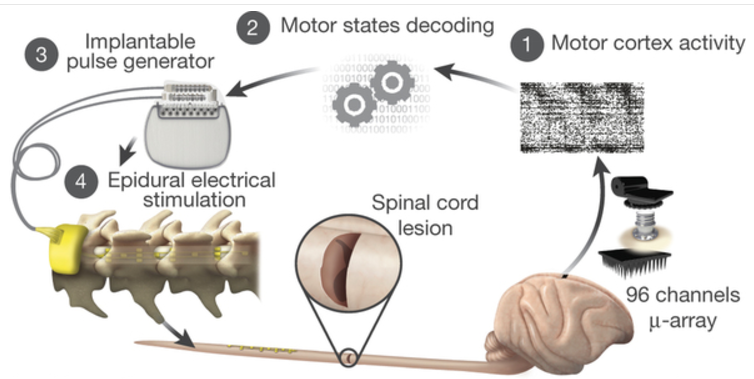
Monkeys were implanted with a microelectrode array into the leg area of the left motor cortex. (1) During recordings, a wireless module transmitted broadband neural signals to a control computer. A raster plot recorded three successive gait cycles. Each line represents spiking events identified from one electrode, while the horizontal axis indicates time. (2) A decoder running on the control computer identified motor states from these neural signals. (3) These motor states triggered electrical spinal cord stimulation protocols, using an implanted pulse generator with real-time triggering capabilities. (4) The stimulator was connected to a spinal implant targeting specific dorsal roots of the lumbar spinal cord. Electromyographic (muscle) signals of an extensor (gray) and flexor (black) muscles acting at the ankle recorded over three successive gait cycles are shown together with a stick diagram decomposition of leg movements during the stance (gray) and swing (black) phases of gait. (credit: Jemère Ruby)

A wireless neurosensor, developed in the neuroengineering lab of Brown University professor Arto Nurmikko, sends the signals gathered by the brain chip wirelessly to a computer that decodes them and sends them wirelessly back to an electrical spinal stimulator implanted in the lumbar spine, below the area of injury.

That electrical stimulation, delivered in patterns coordinated by the decoded brain, sends signals to the spinal nerves that control locomotion.

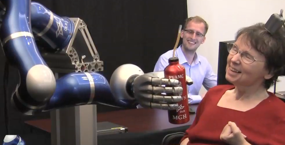
The sensor technology was developed in part for investigational use in humans by the BrainGate collaboration, a research team that includes Brown, Case Western Reserve University, Massachusetts General Hospital, the Providence VA Medical Center, and Stanford University. The technology is being used in ongoing pilot clinical trials, and was used previously in a study in which people with tetraplegia were able to operate a robotic arm simply by thinking about the movement of their own hand. (credit: Brown University)

The ability to transmit brain signals wirelessly was critical to this work with monkeys, the researchers note. Wired brain-sensing systems limit freedom of movement, which in turn limits the information researchers are able to gather about locomotion.

Despite current limitations, the research sets the stage for future studies in primates and, at some point, potentially as a rehabilitation aid in humans, the researchers suggest.

The study, published in the journal Nature, was performed by scientists and neuroengineers in a collaboration led by Ecole Polytechnique Federale Lausanne (EPFL) in Switzerland, together with Brown University, Medtronic and Fraunhofer ICT-IMM in Germany.

The research was funded by European Community’s Seventh Framework Program, International Foundation for Research in Paraplegia Starting Grant from the European Research Council, The Wyss Centre in Geneva Marie Curie Fellowship, Marie Curie COFUND EPFL fellowships, Medtronic Morton Cure Paralysis Fund fellowship, NanoTera.ch Programme (SpineRepair), National Centre of Competence in Research in Robotics Sinergia program, Sino-Swiss Science and Technology Cooperation, and the Swiss National Science Foundation.


Abstract of A brain–spine interface alleviating gait deficits after spinal cord injury in primates

Spinal cord injury disrupts the communication between the brain and the spinal circuits that orchestrate movement. To bypass the lesion, brain–computer interfaces have directly linked cortical activity to electrical stimulation of muscles, and have thus restored grasping abilities after hand paralysis. Theoretically, this strategy could also restore control over leg muscle activity for walking. However, replicating the complex sequence of individual muscle activation patterns underlying natural and adaptive locomotor movements poses formidable conceptual and technological challenges. Recently, it was shown in rats that epidural electrical stimulation of the lumbar spinal cord can reproduce the natural activation of synergistic muscle groups producing locomotion. Here we interface leg motor cortex activity with epidural electrical stimulation protocols to establish a brain–spine interface that alleviated gait deficits after a spinal cord injury in non-human primates. Rhesus monkeys (Macaca mulatta) were implanted with an intracortical microelectrode array in the leg area of the motor cortex and with a spinal cord stimulation system composed of a spatially selective epidural implant and a pulse generator with real-time triggering capabilities. We designed and implemented wireless control systems that linked online neural decoding of extension and flexion motor states with stimulation protocols promoting these movements. These systems allowed the monkeys to behave freely without any restrictions or constraining tethered electronics. After validation of the brain–spine interface in intact (uninjured) monkeys, we performed a unilateral corticospinal tract lesion at the thoracic level. As early as six days post-injury and without prior training of the monkeys, the brain–spine interface restored weight-bearing locomotion of the paralysed leg on a treadmill and overground. The implantable components integrated in the brain–spine interface have all been approved for investigational applications in similar human research, suggesting a practical translational pathway for proof-of-concept studies in people with spinal cord injury.

‘Nanobionic’ spinach plants detect explosives, pollution, drought

By embedding spinach leaves with carbon nanotubes, MIT engineers have transformed spinach plants into sensors that can detect explosives and wirelessly relay that information to a handheld device similar to a smartphone. (credit: Christine Daniloff/MIT)

MIT engineers have implanted spinach leaves with carbon nanotubes, resulting in a hybrid electronic system that they call “plant nanobionics” for detecting dangerous (and other) chemicals.

Two years ago, in the first demonstration of plant nanobionics, MIT engineer Michael Strano, PhD, used nanoparticles to enhance plants’ photosynthesis ability and turn them into sensors for nitric oxide, a pollutant produced by combustion.

Detecting trace molecules

In the new study, the researchers embedded the carbon-nanotube sensors for nitroaromatic compounds into the leaves of spinach plants. The plant can detect minute samples of explosives that leech into the groundwater. Carbon nanotubes can also be used as sensors to detect a wide range of molecules, including hydrogen peroxide, the explosive TNT, and the nerve gas sarin.

To read the signal, the researchers shine a laser onto the leaf, prompting the carbon nanotubes in the leaf to emit near-infrared fluorescent light. This can be detected with a small infrared camera connected to a Raspberry Pi, a $35 credit-card-sized computer, which then alerts the user with an email. The fluorescent signal could also be detected with a smartphone by removing the near-infrared filter that most camera phones have, the researchers say.

“You can apply these techniques with any living plant,” says Strano, leader of the MIT research team and the senior author of a paper describing the nanobionic plants in the Oct. 31 issue of Nature Materials. That opens the door to novel ways for plants to pick up signals that tell of environmental pollution, and even drought.

Plants “know that there is going to be a drought long before we do,” he says. “They can detect small changes in the properties of soil and water potential. If we tap into those chemical signaling pathways, there is a wealth of information to access.”


MIT | Plant-to-human communication


Abstract of Nitroaromatic detection and infrared communication from wild-type plants using plant nanobionics

Plant nanobionics aims to embed non-native functions to plants by interfacing them with specifically designed nanoparticles. Here, we demonstrate that living spinach plants (Spinacia oleracea) can be engineered to serve as self-powered pre-concentrators and autosamplers of analytes in ambient groundwater and as infrared communication platforms that can send information to a smartphone. The plants employ a pair of near-infrared fluorescent nanosensors—single-walled carbon nanotubes (SWCNTs) conjugated to the peptide Bombolitin II to recognize nitroaromatics via infrared fluorescent emission, and polyvinyl-alcohol functionalized SWCNTs that act as an invariant reference signal—embedded within the plant leaf mesophyll. As contaminant nitroaromatics are transported up the roots and stem into leaf tissues, they accumulate in the mesophyll, resulting in relative changes in emission intensity. The real-time monitoring of embedded SWCNT sensors also allows residence times in the roots, stems and leaves to be estimated, calculated to be 8.3 min (combined residence times of root and stem) and 1.9 min mm−1leaf, respectively. These results demonstrate the ability of living, wild-type plants to function as chemical monitors of groundwater and communication devices to external electronics at standoff distances.

Ultra-low-power transistors could function for years without a battery

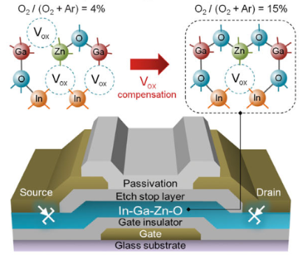
Schematic cross-section of an Indium-gallium-zinc-oxide (IGZO) thin-film transistor [inset: schematic illustrations of atomic structures for less compensated (left) and more compensated (right) IGZO films, respectively] (credit: Sungsik Lee and Arokia Nathan/Science)

Devices based on a new ultra-low-power thin-film transistor design by University of Cambridge engineers could function for months or even years without a battery, by operating on scavenged energy from their environment — ideal for the Internet of Things and for wearable or implantable electronics.

The transistors can be produced at low temperatures and can be printed on almost any material, such as glass, plastic, polyester fabrics, and paper.

Similar to a computer in sleep mode, the new transistor harnesses a tiny “leakage” of electrical current, known as “near-off-state current.” This leak at the point of contact between the metal and semiconducting components of a transistor, the “Schottky barrier,” is normally an undesirable characteristic of all transistors.

The new design gets around one of the main issues preventing the development of ultra-low-power transistors: the ability to produce them at very small sizes. As transistors get smaller, their two electrodes start to influence the behavior of one another, and the voltages spread, causing the transistors to fail to function. By changing the design of the transistors, the Cambridge researchers were able to use the Schottky barriers to keep the electrodes independent from one another, so that the transistors can be scaled down to very small geometries.*

The design also achieves a very high level of gain, or signal amplification. The transistor’s operating voltage is less than one volt, with power consumption below a billionth of a watt. This ultralow power consumption makes them most suitable for applications where function and longevity is more important than speed — as in the Internet of Things.

“If we were to draw energy from a typical AA battery based on this design, it would last for a billion years [ignoring chemical degradation of the battery],” said Sungsik Lee, PhD, first author of the paper in the journal Science.

* “To form a Schottky contact at the source/drain contact of the IGZO TFT, we decreased the electron concentration of the IGZO film by using a high oxygen-gas partial pressure against argon gas, i.e., Pox=O/(O2+ Ar), during the RF sputtering process, with subsequent thermal annealing for a more reliable contact.” — Sungsik Lee and Arokia Nathan/Science


Abstract of Subthreshold Schottky-barrier thin-film transistors with ultralow power and high intrinsic gain

The quest for low power becomes highly compelling in newly emerging application areas related to wearable devices in the Internet of Things. Here, we report on a Schottky-barrier indium-gallium-zinc-oxide thin-film transistor operating in the deep subthreshold regime (i.e., near the OFF state) at low supply voltages (<1 volt) and ultralow power (<1 nanowatt). By using a Schottky-barrier at the source and drain contacts, the current-voltage characteristics of the transistor were virtually channel-length independent with an infinite output resistance. It exhibited high intrinsic gain (>400) that was both bias and geometry independent. The transistor reported here is useful for sensor interface circuits in wearable devices where high current sensitivity and ultralow power are vital for battery-less operation.

‘Bits & Watts’: integrating inexpensive energy sources into the electric grid

Bits & Watts initiative (credit: SLAC National Accelerator Laboratory)

Stanford University and DOE’s SLAC National Accelerator Laboratory launched today an initiative called “Bits & Watts” aimed at integrating low-carbon, inexpensive energy sources, like wind and solar, into the electric grid.

The interdisciplinary initiative hopes to develop “smart” technology that will bring the grid into the 21st century while delivering reliable, efficient, affordable power to homes and businesses.

That means you’ll be able to feed extra power from a home solar collector, for instance, into the grid — without throwing it off balance and triggering potential outages.

The three U.S. power grids (credit: Microsoft Encarta Encyclopedia)

A significant challenge. For starters, the U.S. electric grid is actually two giant, continent-spanning networks, plus a third, smaller network in Texas, that connect power sources and consumers via transmission lines. Each network runs like a single machine, with all its parts humming along at the same frequency, and their operators try to avoid unexpected surges and drops in power that could set off a chain reaction of disruptions and even wreck equipment or hurt people.

Remember the Northeast blackout of 2003, the second largest in history? It knocked out power for an estimated 45 million people in eight U.S. states and 10 million people in the Canadian province of Ontario, some for nearly a week.

“The first challenge was to bring down the cost of wind, solar and other forms of distributed power. The next challenge is to create an integrated system. We must develop the right technologies, financial incentives and investment atmosphere to take full advantage of the lowering costs of clean energy.” — Steven Chu, a Stanford professor, Nobel laureate, former U.S. Energy Secretary, and one of the founding researchers of Bits & Watts. (credit: U.S. Department of Energy)

“Today’s electric grid is … an incredibly complex and finely balanced ecosystem that’s designed to handle power flows in only one direction — from centralized power plants to the consumer,” explained Arun Majumdar, a Stanford professor of mechanical engineering who co-directs both Bits & Watts and the university’s Precourt Institute for Energy, which oversees the initiative.

“As we incorporate more low-carbon, highly variable sources like wind and solar — including energy generated, stored and injected back into the grid by individual consumers — we’ll need a whole new set of tools, from computing and communications to controls and data sciences, to keep the grid stable, efficient and secure and provide affordable electricity.”

Coordination and integration of transmission and distribution systems  (credit: SLAC National Accelerator Laboratory)

The initiative also plans to develop market structures, regulatory frameworks, business models and pricing mechanisms that are crucial for making the grid run smoothly, working with industry and policymakers to identify and solve problems that stand in the way of grid modernization.

(Three bigger grid problems the Stanford announcement today didn’t mention: a geomagnetic solar storm-induced Carrington event, an EMP attack, and a grid cyber attack.)

Simulating the Grid in the Lab

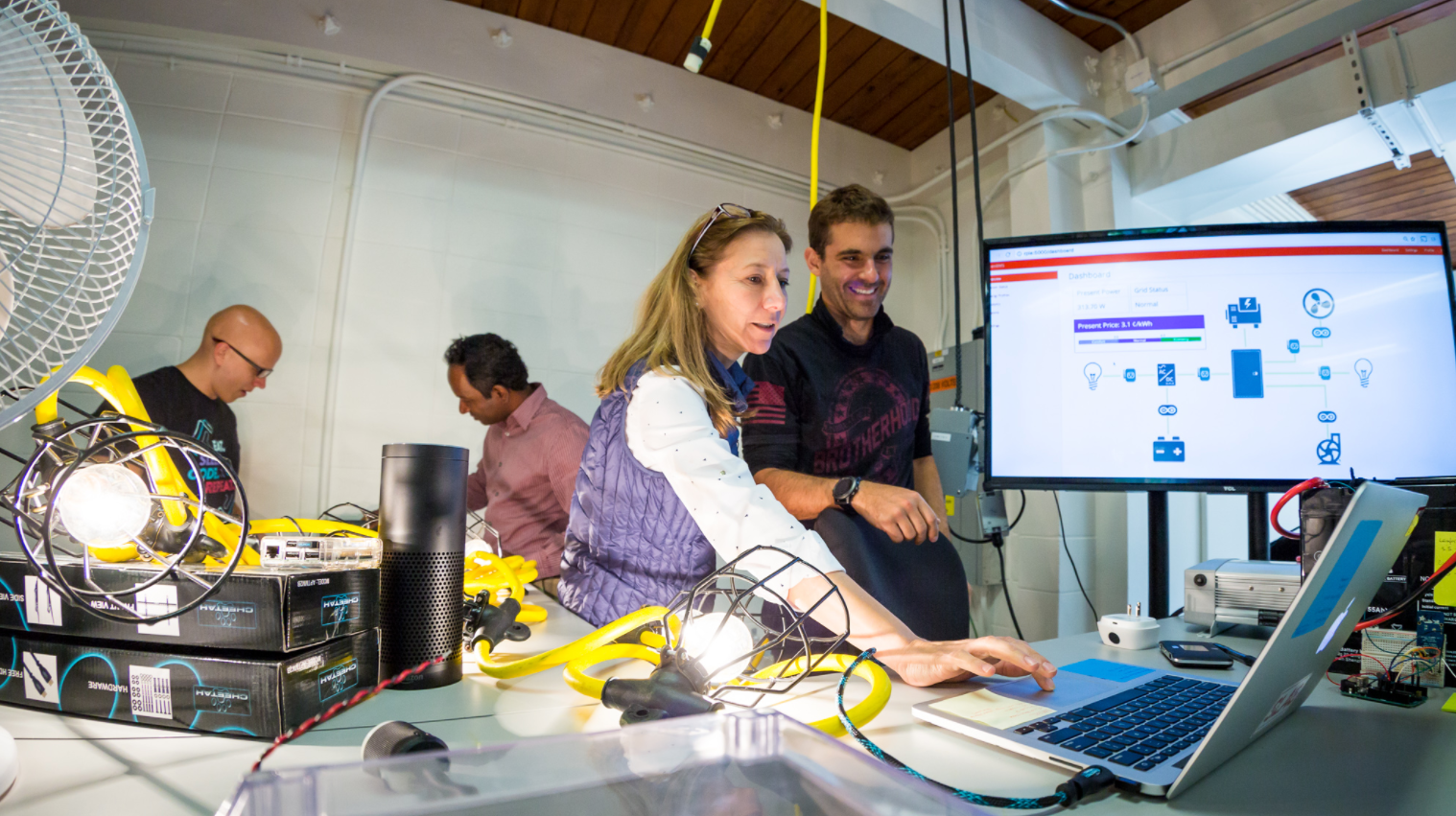
Sila Kiliccote, head of SLAC’s GISMo (Grid Integration, Systems and Mobility) lab, and Stanford graduate student Gustavo Cezar look at a computer dashboard showing how appliances, batteries, lighting and other systems in a “home hub” network could be turned on and off in response to energy prices, consumer preferences and demands on the grid. The lab is part of the Bits & Watts initiative. (credit: SLAC National Accelerator Laboratory)

Researchers will develop ways to use digital sensors and controls to collect data from millions of sources, from rooftop solar panels to electric car charging stations, wind farms, factory operations and household appliances and thermostats, and provide the real-time feedback grid operators need to seamlessly incorporate variable sources of energy and automatically adjust power distribution to customers.

All of the grid-related software developed by Bits & Watts will be open source, so it can be rapidly adopted by industry and policymakers and used by other researchers.

The initiative includes research projects that will:

  • Simulate the entire smart grid, from central power plants to networked home appliances (Virtual Megagrid).
  • Analyze data on electricity use, weather, geography, demographic patterns, and other factors to get a clear understanding of customer behavior via an easy-to-understand graphical interface (VISDOM).
  • Develop a “home hub” system that controls and monitors a home’s appliances, heating and cooling and other electrical demands and can switch them on and off in response to fluctuating electricity prices, demands on the power grid, and the customer’s needs (Powernet).
  • Gather vast and growing sources of data from buildings, rooftop solar modules, electric vehicles, utility equipment, energy markets and so on, and analyze it in real time to dramatically improve the operation and planning of the electricity grid (VADER). This project will incorporate new data science tools such as machine learning, and validate those tools using data from utilities and industry.
  • Create a unique data depository for the electricity ecosystem (DataCommons).

Through the Grid Modernization Initiative, initial Bits & Watts projects are being funded for a combined $8.6 million from two DOE programs, the Advanced Research Projects Agency-Energy (ARPA-E) and the Grid Modernization Laboratory Consortium; $2.2 million from the California Energy Commission; and $1.6 million per year from industrial members, including China State Grid, PG&E (Pacific Gas & Electric), innogy SE (formerly RWE), Schneider Electric and Meidensha Corp.


‘Atomic sandwich’ computing material uses 100 times less energy

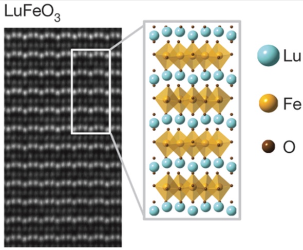
New magnetoelectric multiferroic material operates at 100 times lower power (credit: Julia A. Mundy/Nature)

Lawrence Berkeley National Laboratory scientists have developed a new “magnetoelectric multiferroic*” material that could lead to a new generation of computing devices with more computing power while consuming a fraction of the energy that today’s electronics require.

Electronics could be half of our total global energy consumption by 2030

“Electronics are the fastest-growing consumer of energy worldwide,” said Ramamoorthy Ramesh, associate laboratory director for energy technologies at Lawrence Berkeley National Laboratory.

“Today, about five percent of our total global energy consumption is spent on electronics, and that’s projected to grow to 40–50 percent by 2030 if we continue at the current pace and if there are no major advances in the field that lead to lower energy consumption.”

Global or world energy consumption is the total energy used by all of human civilization. The U.S. Energy Information Administration estimates that in 2013, world energy consumption was 157,481 terawatt hours (TWh), mainly from polluting expendables — oil, coal, and natural gas.

The new material, which combines electrical and magnetic properties at room temperature, could help reduce this consumption in the future.

Room-temperature multiferroics

The newly developed material sandwiches together individual layers of atoms, producing a thin film with magnetic polarity that can be “flipped” from positive to negative or vice versa with small pulses of electricity.

In the future, device makers could use this property to store digital 0’s and 1’s, the binary backbone that underpins computing devices.

“Before this work, there was only one other room-temperature multiferroic whose magnetic properties could be controlled by electricity,” said John Heron, assistant professor in the Department of Materials Science and Engineering at the University of Michigan, who worked on the material with researchers at Cornell University. “That electrical control is what excites electronics makers, so this is a huge step forward.”

100 times less power required

Room-temperature multiferroics are a hotly pursued goal in the electronics field because they require much less power to read and write data than today’s semiconductor-based devices. In addition, they are nonvolatile (their data doesn’t vanish when the power is shut off).

Those properties could enable devices that require only brief pulses of electricity instead of the constant stream that’s needed for current electronics, resulting in using an estimated 100 times less energy.

To create the new material, the researchers started with thin, atomically precise films of hexagonal lutetium iron oxide (LuFeO3), a material known to be a robust ferroelectric, but not strongly magnetic. Lutetium iron oxide consists of alternating monolayers of lutetium oxide and iron oxide. They then used a technique called molecular-beam epitaxy (which takes place in a high vacuum) to add one extra monolayer of iron oxide to every 10 atomic repeats of the single-single monolayer pattern.

“We were essentially spray painting individual atoms of iron, lutetium and oxygen to achieve a new atomic structure that exhibits stronger magnetic properties,” said Darrell Schlom, a materials science and engineering professor at Cornell and senior author of a paper on the work recently published in Nature.

The result was a new material that combines a phenomenon in lutetium oxide called “planar rumpling” with the magnetic properties of iron oxide to achieve multiferroic properties at room temperature.**

While Heron believes a viable multiferroic device is likely several years off, the work puts the field closer to its goal of devices that continue the computing industry’s speed improvements while consuming less power — replacing current silicon-based technology.

The research was published in a paper in the Sept. 22 issue of Nature. It was supported by the Department of Energy’s Office of Science.

* The magnetoelectric effect is the phenomenon of inducing magnetic or electric polarization by applying an external electric or magnetic field. “Ferroics” is the generic name given to the study of iron-based ferromagnetsferroelectrics, and ferroelastics. These materials exhibit large changes in physical characteristics that occur when phase transitions (such as paramagnetic, or temporary magnetism, to ferromagnetic, or permanent magnetism) take place around some critical temperature value. Multiferroics exhibit more than one ferroic property simultaneously.

** Heron explains that the lutetium exhibits atomic-level displacements called rumples. Visible under an electron microscope, the rumples enhance the magnetism in the material, allowing it to persist at room temperature. The rumples can be moved by applying an electric field, and are enough to nudge the magnetic field in the neighboring layer of iron oxide from positive to negative or vice versa, creating a material whose magnetic properties can be controlled with electricity — a “magnetoelectric multiferroic.”


Abstract of Atomically engineered ferroic layers yield a room-temperature magnetoelectric multiferroic

Materials that exhibit simultaneous order in their electric and magnetic ground states hold promise for use in next-generation memory devices in which electric fields control magnetism. Such materials are exceedingly rare, however, owing to competing requirements for displacive ferroelectricity and magnetism. Despite the recent identification of several new multiferroic materials and magnetoelectric coupling mechanisms, known single-phase multiferroics remain limited by antiferromagnetic or weak ferromagnetic alignments, by a lack of coupling between the order parameters, or by having properties that emerge only well below room temperature, precluding device applications2. Here we present a methodology for constructing single-phase multiferroic materials in which ferroelectricity and strong magnetic ordering are coupled near room temperature. Starting with hexagonal LuFeO3—the geometric ferroelectric with the greatest known planar rumpling—we introduce individual monolayers of FeO during growth to construct formula-unit-thick syntactic layers of ferrimagnetic LuFe2O4 within the LuFeO3 matrix, that is, (LuFeO3)m/(LuFe2O4)1 superlattices. The severe rumpling imposed by the neighbouring LuFeO3 drives the ferrimagnetic LuFe2O4 into a simultaneously ferroelectric state, while also reducing the LuFe2O4 spin frustration. This increases the magnetic transition temperature substantially—from 240 kelvin for LuFe2O4to 281 kelvin for (LuFeO3)9/(LuFe2O4)1. Moreover, the ferroelectric order couples to the ferrimagnetism, enabling direct electric-field control of magnetism at 200 kelvin. Our results demonstrate a design methodology for creating higher-temperature magnetoelectric multiferroics by exploiting a combination of geometric frustration, lattice distortions and epitaxial engineering.

Bendable electronic color ‘paper’ invented

Chalmers’ e-paper contains gold, silver and PET plastic. The layer that produces the colors is less than a micrometer thin. (credit: Mats Tiborn)

Chalmers University of Technology researchers have developed the basic technology for a new kind of reflective electronic “paper” that is micrometer-thin and bendable. It can display all colors displayed on an LED display, but with one tenth the energy required with a Kindle tablet.

This Chalmers logotype shows how RGB pixels can reproduce color images. The magnification shows which pixels are activated to create elements of the image. (credit: Kunli Xiong)

The technology is based on electrically controllable optical absorption of a conducting polymer, which is used to modulate the reflected light from ultrathin nanostructured plasmonic metasurfaces. (KurzweilAI has covered a number of research projects using reflective plasmonic designs, such as this one and this one.)

The plasmonic metasurfaces. (a) Schematic of the plasmonic metasurface, which has three layers. A 150 nm silver film was first deposited on the substrate to provide a high base reflection. The next alumina spacer layer tuned the reflective color by Fabry–Pérot interference. (b) Then 150 nm nanoholes in a 20 nm gold film were prepared on alumina by colloidal self-assembly and tape stripping. (c) The color palette was created by varying the alumina thickness for the primary colors red, green, and blue, corresponding to an alumina thickness of 48, 93, and 83 nm respectively. (d) A photo of samples with the primary colors under ambient light. (credit: Kunli Xiong et al./Advanced Materials)

“The ‘paper’ is similar to the Kindle tablet,” says Chalmers researcher Andreas Dahlin. “It isn’t lit up like a standard display, but rather reflects the external light which illuminates it. Therefore it works very well where there is bright light, such as out in the sun, in contrast to standard LED displays that work best in darkness. At the same time it needs only a tenth of the energy that a Kindle tablet uses, which itself uses much less energy than a tablet LED display.”

The material is not yet ready for production. One obstacle is that there is gold and silver in the display, which makes the manufacturing expensive, Dahlin explains.

He says optimal applications for the displays will be well-lit places such as outside or in public places for displaying information. This could reduce the energy consumption and at the same time replace signs and information screens that aren’t currently electronic today with more flexible ones.


Abstract of Plasmonic Metasurfaces with Conjugated Polymers for Flexible Electronic Paper in Color

A flexible electronic paper in full color is realized by plasmonic metasurfaces with conjugated polymers. An ultrathin large-area electrochromic material is presented which provides high polarization-independent reflection, strong contrast, fast response time, and long-term stability. This technology opens up for new electronic readers and posters with ultralow power consumption.

Engineers reveal fabrication process for revolutionary transparent graphene neural sensors

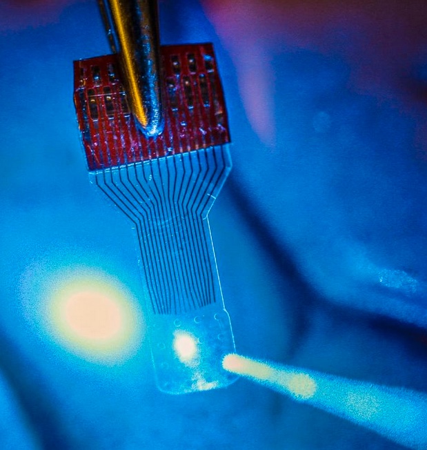
A blue light shines through a transparent, implantable medical sensor onto a brain. The invention may help neural researchers better view brain activity. (credit: Justin Williams research group)

In an open-access paper published Thursday (Oct. 13, 2016) in the journal Nature Protocols, University of Wisconsin–Madison engineers have published details of how to fabricate and use neural microelectrocorticography (μECoG) arrays made with transparent graphene in applications in electrophysiology, fluorescent microscopy, optical coherence tomography, and optogenetics.

Graphene is one of the most promising candidates for transparent neural electrodes, because the material has a UV to IR transparency of more than 90%, in addition to its high electrical and thermal conductivity, flexibility, and biocompatibility, the researchers note in the paper. That allows for simultaneous high-resolution imaging and optogenetic control.

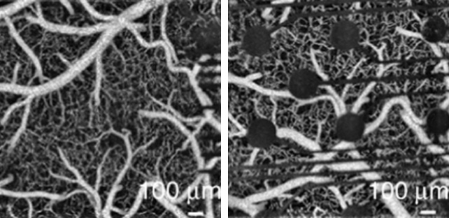
Left: Optical coherence tomography (OCT) image captured through an implanted transparent graphene electrode array, allowing for simultaneous observation of cells immediately beneath electrode sites during optical or electrical stimulation. Right: Optical coherence tomography (OCT) image taken with an implanted conventional opaque platinum electrode array. (credit: Dong-Wook Park et al./Nature Protocols)

The procedures in the paper are for a graphene μECoG electrode array implanted on the surface of the cerebral cortex and can be completed within 3–4 weeks by an experienced graduate student, according to the researchers. But this protocol “may be amenable to fabrication and testing of a multitude of other electrode arrays used in biological research, such as penetrating neural electrode arrays to study deep brain, nerve cuffs that are used to interface with the peripheral nervous system (PNS), or devices that interface with the muscular system,” according to the paper.

The researchers first announced the breakthrough in the open-access journal Nature Communications in 2014, as KurzweilAI reported. Now, the UW–Madison researchers are looking at ways to improve and build upon the technology. They also are seeking to expand its applications from neuroscience into areas such as research of stroke, epilepsy, Parkinson’s disease, cardiac conditions, and many others. And they hope other researchers do the same.

Funding for the initial research came from the Reliable Neural-Interface Technology program at the U.S. Defense Advanced Research Projects Agency.

The research was led by Zhenqiang (Jack) Ma, the Lynn H. Matthias Professor and Vilas Distinguished Achievement Professor in electrical and computer engineering at UW–Madison and Justin Williams, the Vilas Distinguished Achievement Professor in biomedical engineering and neurological surgery at UW–Madison.

Researchers at the University of Wisconsin-Milwaukee, Medtronic PLC Neuromodulation, the University of Washington, and Mahidol University in Bangkok, Thailand were also involved.


Abstract of Fabrication and utility of a transparent graphene neural electrode array for electrophysiology, in vivo imaging, and optogenetics

Transparent graphene-based neural electrode arrays provide unique opportunities for simultaneous investigation of electrophysiology, various neural imaging modalities, and optogenetics. Graphene electrodes have previously demonstrated greater broad-wavelength transmittance (~90%) than other transparent materials such as indium tin oxide (~80%) and ultrathin metals (~60%). This protocol describes how to fabricate and implant a graphene-based microelectrocorticography (μECoG) electrode array and subsequently use this alongside electrophysiology, fluorescence microscopy, optical coherence tomography (OCT), and optogenetics. Further applications, such as transparent penetrating electrode arrays, multi-electrode electroretinography, and electromyography, are also viable with this technology. The procedures described herein, from the material characterization methods to the optogenetic experiments, can be completed within 3–4 weeks by an experienced graduate student. These protocols should help to expand the boundaries of neurophysiological experimentation, enabling analytical methods that were previously unachievable using opaque metal–based electrode arrays.