Berkeley Lab announces first transistor with a working 1-nanometer gate

Schematic of a transistor with molybdenum disulfide semiconductor and 1-nanometer carbon nanotube gate. (credit: Sujay Desai/Berkeley Lab)

The first transistor with a working 1-nanometer (nm) gate* has been created by a team led by Lawrence Berkeley National Laboratory (Berkeley Lab) scientists. Until now, a transistor gate size less than 5 nanometers has been considered impossible because of quantum tunneling effects. (One nanometer is the diameter of a glucose molecule.)

The breakthrough was achieved by creating a 2D (flat) semiconductor field-effect transistor using molybdenum disulfide (MoS2) instead of silicon and a 1D single-walled carbon nanotube (SWCNT) as a gate electrode, instead of various metals. (SWCNTs are hollow cylindrical tubes with diameters as small as 1 nanometer.)

The MoS2 advantage

Compared with MoS2, electrons flowing through silicon are lighter and encounter less resistance . But with a gate length below 5 nanometers in length, a quantum mechanical phenomenon called tunneling kicks in, and the gate barrier is no longer able to keep the electrons from barging through from the source to the drain terminals, so the transistor cannot be turned off.

Electrons flowing through MoS2 are heavier, so their flow can be controlled with smaller gate lengths. MoS2 can also be scaled down to atomically thin sheets, about 0.65 nanometers thick, with a a larger band gap and lower dielectric constant, a measure reflecting the ability of a material to store energy in an electric field (similar to a capacitor). These properties help improve the control of the flow of current inside the transistor when the gate length is reduced to 1 nanometer.

Transistors consist of three terminals: a source (left), a drain (right), and a gate (the carbon nanotube, black, below). Current flows through the semiconductor (MoS2, represented by the yellow molecular model) from the source to the drain. Based on the voltage applied to the gate, it switches the channel (the portion of the MoS2 semiconductor just above the carbon nanotube) on and off, via a dielectric (zirconium oxide, green), operating in a manner similar to a capacitor. (credit: Sujay Desai/Berkeley Lab)

“We made the smallest transistor reported to date,” said faculty scientist Ali Javey at the Department of Energy’s Lawrence Berkeley National Laboratory (Berkeley Lab) and lead principal investigator of the Electronic Materials program in Berkeley Lab’s Materials Science Division. “The gate length is considered a defining dimension of the transistor. We demonstrated a 1-nanometer-gate transistor, showing that with the choice of proper materials, there is a lot more room to shrink our electronics.”

The development could be key to keeping alive Intel co-founder Gordon Moore’s prediction that the density of transistors on integrated circuits would double every two years, enabling the increased performance of our laptops, mobile phones, televisions, and other electronics.

“The semiconductor industry has long assumed that any gate below 5 nanometers wouldn’t work, so anything below that was not even considered,” said study lead author Sujay Desai, a graduate student in Javey’s lab. “This research shows that sub-5-nanometer gates should not be discounted. Industry has been squeezing every last bit of capability out of silicon. By changing the material from silicon to MoS2, we can make a transistor with a gate that is just 1 nanometer in length, and operate it like a switch.”

Transmission electron microscope image of a cross section of the transistor, showing the edge of a 1-nanometer carbon nanotube gate and the molybdenum disulfide semiconductor separated by zirconium dioxide, which is a dielectric insulator. (credit: Sujay B. Desai/Science)

Continuing Moore’s law

“This work demonstrated the shortest transistor ever,” said Javey, who is also a UC Berkeley professor of electrical engineering and computer sciences. “However, it’s a proof of concept. We have not yet packed these transistors onto a chip, and we haven’t done this billions of times over. We also have not developed self-aligned fabrication schemes for reducing parasitic resistances in the device. But this work is important to show that we are no longer limited to a 5-nanometer gate for our transistors. Moore’s Law can continue a while longer by proper engineering of the semiconductor material and device architecture.”

The findings appeared in the Oct. 7 issue of the journal Science. Researchers at the University of Texas at Dallas, Stanford University, and  the University of California, Berkeley, were also involved. The work at Berkeley Lab was primarily funded by the Department of Energy’s Basic Energy Sciences program.

According to an earlier article in CTimes on Sept. 30, Taiwan Semiconductor Manufacturing Co., Ltd. (TSMC) said the company is working toward a 1-nanometer manufacturing process, starting with a “5 nanometers process technology, while putting about 300 to 400 R&D personnel in developing more advanced 3-nanometer process.” However, TSMC spokesperson Elizabeth Sun told KurzweilAI that “no further information regarding any technology either under development or in path-finding stage will be disclosed to the public at this point.”

* Gate length is the length of the gate portion of the transistor, not to be confused with “node,” which was initially a measure of “half pitch” (half of the distance between features of a transistor), but the number itself has lost the exact meaning it once held. Gate length was 26nm for the 22nm node from Intel and 20 nanometers for the more recent 14nm node from Intel. — S. Natarajan et al., “A 14nm logic technology featuring 2nd-generation FinFET, air-gapped interconnects, self-aligned double patterning and a 0.0588 µm2 SRAM cell size,” 2014 IEEE International Electron Devices Meeting, San Francisco, CA, 2014, pp. 3.7.1-3.7.3. doi: 10.1109/IEDM.2014.7046976


Abstract of MoS2 transistors with 1-nanometer gate lengths

Scaling of silicon (Si) transistors is predicted to fail below 5-nanometer (nm) gate lengths because of severe short channel effects. As an alternative to Si, certain layered semiconductors are attractive for their atomically uniform thickness down to a monolayer, lower dielectric constants, larger band gaps, and heavier carrier effective mass. Here, we demonstrate molybdenum disulfide (MoS2) transistors with a 1-nm physical gate length using a single-walled carbon nanotube as the gate electrode. These ultrashort devices exhibit excellent switching characteristics with near ideal subthreshold swing of ~65 millivolts per decade and an On/Off current ratio of ~106. Simulations show an effective channel length of ~3.9 nm in the Off state and ~1 nm in the On state.

Genetically engineered peptides on 2D nanosheets form bio-nano interfaces

A top view of GrBP5 nanowires on a 2-D surface of graphene (credit: Mehmet Sarikaya/Scientific Reports)

Engineers at the University of Washington have created genetically engineered peptides that self-assemble into arrays of nanowires on two-dimensional nanosheets (single-layer graphene and molybdenum disulfide) to relay information across a bio-nano interface — a first step towards fully self-assembled future biomedical and electro-optical bionanoelectronic devices.

Arrays of peptides could provide organized scaffolds for functional biomolecules, enabling nanoscale bioelectronics interfaces. And designed peptides could be incorporated with metal ions or nanoparticles with specific physical characteristics, thus fine-tuning 2D device performance for chemical and biological sensors.

A bridge between biology and technology

“Bridging this divide would be the key to building the genetically engineered biomolecular solid-state devices of the future,” said UW professor Mehmet Sarikaya in the Departments of Materials Science & Engineering, senior author of an open-access paper published Sept. 22 in Scientific Reports.

The UW team is also planning to develop genetically engineered peptides with specific chemical and structural properties. Their ideal peptide would change the physical properties of synthetic materials and respond to that change. That way, it would transmit “information” from the synthetic material to other biomolecules — bridging the chemical divide between biology and technology.

The peptides function through molecular recognition — the same principles that underlie biochemical interactions such as an antibody binding to its specific antigen or protein binding to DNA.

A schematic showing GrBP5 peptide self-organization with a series of surface processes on graphene: binding, diffusion and self-organization (credit: Yuhei Hayamizu et al./Scientific Reports)

In exploring the properties of 80 genetically selected peptides — which are not found in nature but have the same chemical components as peptides in all proteins — the researchers discovered that one peptide, GrBP5, showed promising interactions with the semimetal graphene. They tested GrBP5’s interactions with several other 2-D nanomaterials that “could serve as the metals or semiconductors of the future,” Sarikaya said.

Their experiments revealed that GrBP5 spontaneously organized into ordered nanowire patterns on graphene. With a few mutations, GrBP5 also altered the electrical conductivity of a graphene-based device, the first step toward transmitting electrical information from graphene to cells via peptides.

New bio-optoelectronic devices

Sarikaya’s team also modified GrBP5 to produce similar results on semiconductor material molybdenum disulfide (MoS2) and other materials* by converting a chemical signal to an optical signal. And they computationally predicted how different arrangements of GrBP5 nanowires would affect the electrical conduction or optical signal properties of each material.

A top view image of GrBP5 nanowires on a 2-D surface of molybdenum disulfide (credit: Mehmet Sarikaya/Scientific Reports)

The researchers are also seeking a peptide that could interact with materials such as gold, titanium, and even a mineral in bone and teeth.

Funded by the National Science Foundation, the UW, the National Institutes of Health, and the Japan Science and Technology Agency, the research is the focus of a new endeavor funded by the National Science Foundation’s Materials Genome Initiative. UW’s CoMotion is also working with Amazon to develop nano-sensors to detect early stages of pancreatic cancer.

* Other semiconducting 2D transition metal dichalcogenides (WSe2, WS2, MoSe2) along with insulating hBN, all with unique electronic and optical properties, were also tested.


Abstract of Bioelectronic interfaces by spontaneously organized peptides on 2D atomic single layer materials

Self-assembly of biological molecules on solid materials is central to the “bottom-up” approach to directly integrate biology with electronics. Inspired by biology, exquisite biomolecular nanoarchitectures have been formed on solid surfaces. We demonstrate that a combinatorially-selected dodecapeptide and its variants self-assemble into peptide nanowires on two-dimensional nanosheets, single-layer graphene and MoS2. The abrupt boundaries of nanowires create electronic junctions via spatial biomolecular doping of graphene and manifest themselves as a self-assembled electronic network. Furthermore, designed peptides form nanowires on single-layer MoS2 modifying both its electric conductivity and photoluminescence. The biomolecular doping of nanosheets defined by peptide nanostructures may represent the crucial first step in integrating biology with nano-electronics towards realizing fully self-assembled bionanoelectronic devices.

Synapse-like memristor-based electronic device detects brain spikes in real time

Memristor chip (credit: University of Southampton)

A bio-inspired electronic device called a memristor could allow for real-time processing of neuronal signals (spiking events), new research led by the University of Southampton has demonstrated.

The research could lead to using multi-electrode array implants for detecting spikes in the brain’s electrical signals from more than 1,000 recording channels to help treat neurological conditions, without requiring expensive, high-bandwidth, bulky systems for processing data. The research could lead to future autonomous, fully implantable neuroprosthetic devices.

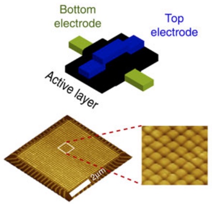
Schematic illustration of a solid-state titanium-oxide memristive device and atomic force microscopic (AFM) image a portion of a 32 × 32 crossbar array of memristors (credit: Isha Gupta/Nature Communications)

A memristors is an electronic component that limits or regulates the flow of electrical current in a circuit, can remember the amount of charge that was flowing through it, and retain that data, even when the power is turned off. The researchers used an array of memristors.

The research team designed a new nanoscale device they called a “memristive integrating sensor” (MIS) based on a memristors and associated electronic circuits for detecting spikes.*

Acting like synapses in the brain, the MIS was able to encode and compress (up to 200 times) neuronal spiking activity recorded by multi-electrode arrays. Besides addressing the bandwidth constraints, this approach was also very power-efficient; the power needed per recording channel was up to 100 times less when compared to current best practice.

The research was published in the open-access journal Nature Communications.

The Prodromakis Group at the University of Southampton collaborated among others with Leon Chua (a Diamond Jubilee Visiting Academic at the University of Southampton), who theoretically predicted the existence of memristors in 1971.

This interdisciplinary work was supported by an FP7 project (the European Union’s Research and Innovation funding) and brought together engineers from the Nanoelectronics and Nanotechnology Group at the University of Southampton with biologists from the University of Padova and the Max Planck Institute, Germany, using the state-of-art facilities of the Southampton Nanofabrication Centre.

* The paper explains that signals from an array of neural electrodes are fed into the MIS system as a series of voltage-time samples. “The MIS begins by pre-amplifying the incoming signal to voltage levels suitable for operating the memristor sitting at the core of the MIS and then proceeding to apply the pre-amplified signals to the memristor in real-time. The memristor’s resistive state is assessed periodically and when a significant change in comparison to the previous state is detected, the system registers a spiking event.”


Abstract of Real-time encoding and compression of neuronal spikes by metal-oxide memristors

Advanced brain-chip interfaces with numerous recording sites bear great potential for investigation of neuroprosthetic applications. The bottleneck towards achieving an efficient bio-electronic link is the real-time processing of neuronal signals, which imposes excessive requirements on bandwidth, energy and computation capacity. Here we present a unique concept where the intrinsic properties of memristive devices are exploited to compress information on neural spikes in real-time. We demonstrate that the inherent voltage thresholds of metal-oxide memristors can be used for discriminating recorded spiking events from background activity and without resorting to computationally heavy off-line processing. We prove that information on spike amplitude and frequency can be transduced and stored in single devices as non-volatile resistive state transitions. Finally, we show that a memristive device array allows for efficient data compression of signals recorded by a multi-electrode array, demonstrating the technology’s potential for building scalable, yet energy-efficient on-node processors for brain-chip interfaces.

How to send secure passwords through your body instead of air

Potential applications for on-body transmissions include securely sending information to door locks, glucose sensors, or other wearable medical devices. (credit: Vikram Iyer, University of Washington)

University of Washington computer scientists and electrical engineers have devised a way to send secure passwords through the human body, using benign, low-frequency transmissions already generated by fingerprint sensors and touchpads on consumer devices.

“Let’s say I want to open a door using an electronic smart lock,” said Merhdad Hessar, a UW electrical engineering doctoral student and co-lead author of a paper presented in September at the 2016 Association for Computing Machinery’s International Joint Conference on Pervasive and Ubiquitous Computing (UbiComp 2016) in Germany. “I can touch the doorknob and touch the fingerprint sensor on my phone and transmit my secret credentials through my body to open the door, without leaking that personal information over the air.”

Secure on-body transmissions

These “on-body” transmissions offer a more secure way to transmit authenticating information between devices that touch parts of your body — such as a wearable medical device — and a phone or device that confirms your identity by asking you to type in a password.

The technology could also be useful for secure key transmissions to medical devices which seek to confirm someone’s identity before sending or sharing data, such as glucose monitors or insulin pumps.

The research team tested the technique on iPhone and other fingerprint sensors, as well as Lenovo laptop trackpads and the Adafruit capacitive touchpad. In tests with ten different subjects, they were able to generate usable on-body transmissions on people of different heights, weights and body types. The system also worked when subjects were in motion, including while they walked and moved their arms.

The researchers showed that it works in different postures like standing, sitting and sleeping, and they can get a strong signal throughout your body, with receivers on any part of the body.

Reverse-engineering and repurposing smartphone sensors

The research team from the UW’s Networks and Mobile Systems Lab systematically analyzed smartphone sensors to understand which of them generates low-frequency transmissions below 30 megahertz (which travel well through the human body but don’t propagate over the air).

The researchers found that fingerprint sensors and touchpads generate signals in the 2 to 10 megahertz range and employ capacitive coupling to sense where your finger is in space and to identify the ridges and valleys that form unique fingerprint patterns.

Normally, sensors use these signals to receive input about your finger. But the UW engineers devised a way to use these signals as output that corresponds to data contained in a password or access code. When entered on a smartphone, data that authenticates your identity can travel securely through your body to a receiver embedded in a device that needs to confirm who you are.

Their process employs a sequence of finger scans to encode and transmit data. Performing a finger scan correlates to a 1-bit of digital data and not performing the scan correlates to a 0-bit. The team achieved bit rates of 50 bits per second on laptop touchpads and 25 bits per second with fingerprint sensors — fast enough to send a simple password or numerical code through the body and to a receiver within seconds.

This represents only a first step, the researchers say. Data can be transmitted through the body even faster if fingerprint sensor manufacturers provide more access to their software.

The research was funded by the Intel Science and Technology Center for Pervasive Computing, a Google faculty award and the National Science Foundation.

For more information, contact the research team at onbody@cs.washington.edu.


Abstract of Enabling on-body transmissions with commodity devices

We show for the first time that commodity devices can be used to generate wireless data transmissions that are confined to the human body. Specifically, we show that commodity input devices such as fingerprint sensors and touchpads can be used to transmit information to only wireless receivers that are in contact with the body. We characterize the propagation of the resulting transmissions across the whole body and run experiments with ten subjects to demonstrate that our approach generalizes across different body types and postures. We also evaluate our communication system in the presence of interference from other wearable devices such as smartwatches and nearby metallic surfaces. Finally, by modulating the operations of these input devices, we demonstrate bit rates of up to 50 bits per second over the human body.

How to detect emotions remotely with wireless signals


MITCSAIL | EQ-Radio: Emotion Recognition using Wireless Signals

MIT researchers from have developed “EQ-Radio,” a device that can detect a person’s emotions using wireless signals.

By measuring subtle changes in breathing and heart rhythms, EQ-Radio is 87 percent accurate at detecting if a person is excited, happy, angry or sad — and can do so without on-body sensors, according to the researchers.

MIT professor and project lead Dina Katabi of MIT’s Computer Science and Artificial Intelligence Laboratory (CSAIL) envisions the system being used in health care and testing viewers’ reactions to ads or movies in real time.

Using wireless signals reflected off people’s bodies, the device measures heartbeats as accurately as an ECG monitor, with a margin of error of approximately 0.3 percent, according to the researchers. It then studies the waveforms within each heartbeat to match a person’s behavior to how they previously acted in one of the four emotion-states.

The team will present the work next month at the Association of Computing Machinery’s International Conference on Mobile Computing and Networking (MobiCom).

How it works

EQ-Radio has three components: a radio for capturing RF reflections, a heartbeat extraction algorithm, and a classification subsystem that maps the learned physiological signals to emotional states. (credit: Mingmin Zhao et al./MIT)

EQ-Radio sends wireless signals that reflect off of a person’s body and back to the device. To detect emotions, its beat-extraction algorithms break the reflections into individual heartbeats and analyze the small variations in heartbeat intervals to determine their levels of arousal and positive affect.

These measurements are what allow EQ-Radio to detect emotion. For example, a person whose signals correlate to low arousal and negative affect is more likely to tagged as sad, while someone whose signals correlate to high arousal and positive affect would likely be tagged as excited.

The exact correlations vary from person to person, but are consistent enough that EQ-Radio could detect emotions with 70 percent accuracy even when it hadn’t previously measured the target person’s heartbeat. In the future it could be used for non-invasive health monitoring and diagnostic settings.

For the experiments, subjects used videos or music to recall a series of memories that each evoked one the four emotions, as well as a no-emotion baseline. Trained just on those five sets of two-minute videos, EQ-Radio could then accurately classify the person’s behavior among the four emotions 87 percent of the time.

One of the challenges was to tune out irrelevant data. To get individual heartbeats, for example, the team had to dampen the breathing, since the distance that a person’s chest moves from breathing is much greater than the distance that their heart moves to beat.

To do so, the team focused on wireless signals that are based on acceleration rather than distance traveled, since the rise and fall of the chest with each breath tends to be much more consistent —  and, therefore, have a lower acceleration — than the motion of the heartbeat.


Abstract of Emotion Recognition using Wireless Signals

This paper demonstrates a new technology that can infer a person’s emotions from RF signals reflected off his body. EQ-Radio transmits an RF signal and analyzes its reflections off a person’s body to recognize his emotional state (happy, sad, etc.). The key enabler underlying EQ-Radio is a new algorithm for extracting the individual heartbeats from the wireless signal at an accuracy comparable to on-body ECG monitors. The resulting beats are then used to compute emotion-dependent features which feed a machine-learning emotion classifier. We describe the design and implementation of EQ-Radio, and demonstrate through a user study that its emotion recognition accuracy is on par with stateof-the-art emotion recognition systems that require a person to be hooked to an ECG monitor.

Self-powered ‘materials that compute’ and recognize simple patterns

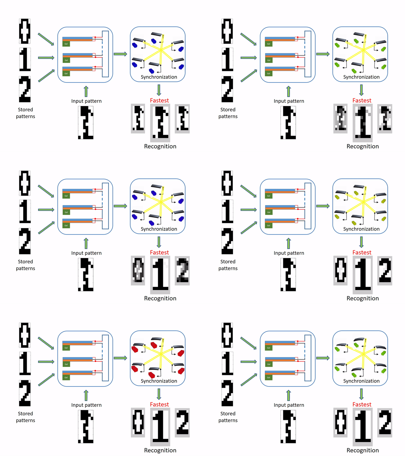
Conceptual illustration of pattern recognition process performed by hybrid gel-piezoelectric oscillator system (credit: Yan Fang)

University of Pittsburgh researchers have modeled the design of a “material that computes” — a hybrid material, powered only by its own chemical reactions, that can recognize simple patterns.

The material could one day be integrated into clothing and used to monitor the human body, or developed as a skin for “squishy” robots, for example, according to the researchers, writing in the open-access AAAS journal Science Advances.

A computer that combines gels and piezeoelectric materials

The computations (needed to design the hypothetical material) were modeled utilizing Belousov-Zhabotinsky (BZ) gels, a substance that oscillates in the absence of external stimuli, combined with an overlaying piezoelectric (PZ) cantilever, forming “BZ-PZ” (as in “easy peasy”). The BZ gels oscillate periodically, triggered by chemical stimulation, without the need for external driving stimuli. Piezoelectric (PZ) materials generate a voltage when deformed and, conversely, undergo deformation in the presence of an applied voltage.

Two BZ-PZ oscillator units connected with electrical wires. Triggered by the chemical oscillations, the BZ gels (green) expand in volume, generating a force (F1 and F2) and thereby cause the deflections ξ1 and ξ2 of the PZ cantilevers (orange and blue layers) , which generate an electric voltage U. That voltage then deflects the cantilevers (the inverse PZ effect), which then compress the underlying BZ gels and thereby modify the chemomechanical oscillations in these gels. The end result is the components’ response to self-generated signals (sensing), volumetric changes in the gel (actuation), and the passage of signals between the units (communication). For computation, the communication also leads to synchronization of the BZ gel oscillators. (credit: Yan Fang et al./Science Advances)

“By combining these attributes into a ‘BZ-PZ’ unit and then connecting the units by electrical wires, we designed a device that senses, actuates, and communicates without an external electrical power source,” the researchers explain in the paper.*

The result is that the device can also be used to perform computation. To use that for pattern recognition, the researchers first stored a pattern of numbers as a set of polarities in the BZ-PZ units, and the input patterns were coded with the initial phase of the oscillations imposed on these units.

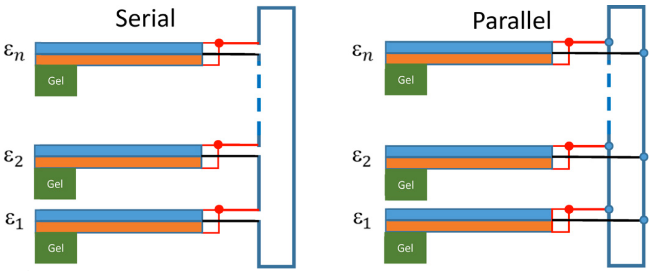
Multiple BZ-PS units wired in serial and parallel configurations to form a network (credit: Yan Fang et al./Science Advances)

With multiple BZ-PZ units, the oscillators can be wired into a network  formed, for example, from units that are connected in parallel or in series. The resulting transduction between chemomechanical and electrical energy creates signals that quickly propagate and thus permits remote coupled oscillators to communicate and synchronize. This synchronization behavior in BZ-PZ network can be used for oscillator-based computing.

The computational modeling revealed that the input pattern closest to the stored pattern exhibits the fastest convergence time to the stable synchronization behavior, and is the most effective at recognizing patterns. In this study, the materials were programmed to recognize black-and-white pixels in the shape of numbers that had been distorted.

The researchers’ next goal is to expand from analyzing black-and-white pixels to grayscale and more complicated images and shapes, as well as to enhance the devices storage capability.

Perfect for monitoring human and robot bodies

Compared to a traditional computer, these computations are slow and take minutes. “Individual events are slow because the period of the BZ oscillations is slow,” said Victor V. Yashin, Research Assistant Professor of Chemical and Petroleum Engineering. “However, there are some tasks that need a longer analysis, and are more natural in function. That’s why this type of system is perfect to monitor environments like the human body.”

For example, Dr. Yashin said that patients recovering from a hand injury could wear a glove that monitors movement, and can inform doctors whether the hand is healing properly or if the patient has improved mobility. Another use would be to monitor individuals at risk for early onset Alzheimer’s, by wearing footwear that would analyze gait and compare results against normal movements, or a garment that monitors cardiovascular activity for people at risk of heart disease or stroke.

Since the devices convert chemical reactions to electrical energy, there would be no need for external electrical power. This would also be ideal for a robot or other device that could utilize the material as a sensory skin.

The research is funded by a five-year National Science Foundation Integrated NSF Support Promoting Interdisciplinary Research and Education (INSPIRE) grant, which focuses on complex and pressing scientific problems that lie at the intersection of traditional disciplines.

“This work at the University of Pittsburgh … is an example of this groundbreaking shift away from traditional silicon CMOS-based digital computing to a non-von Neumann machine in a polymer substrate, with remarkable low power consumption,” said Sankar Basu, NSF program director.

* This continues the research of Anna C. Balazs, Distinguished Professor of Chemical and Petroleum Engineering, and Steven P. Levitan, the John A. Jurenko Professor of Electrical and Computer Engineering. 


Abstract of Pattern recognition with “materials that compute”

Driven by advances in materials and computer science, researchers are attempting to design systems where the computer and material are one and the same entity. Using theoretical and computational modeling, we design a hybrid material system that can autonomously transduce chemical, mechanical, and electrical energy to perform a computational task in a self-organized manner, without the need for external electrical power sources. Each unit in this system integrates a self-oscillating gel, which undergoes the Belousov-Zhabotinsky (BZ) reaction, with an overlaying piezoelectric (PZ) cantilever. The chemomechanical oscillations of the BZ gels deflect the PZ layer, which consequently generates a voltage across the material. When these BZ-PZ units are connected in series by electrical wires, the oscillations of these units become synchronized across the network, where the mode of synchronization depends on the polarity of the PZ. We show that the network of coupled, synchronizing BZ-PZ oscillators can perform pattern recognition. The “stored” patterns are set of polarities of the individual BZ-PZ units, and the “input” patterns are coded through the initial phase of the oscillations imposed on these units. The results of the modeling show that the input pattern closest to the stored pattern exhibits the fastest convergence time to stable synchronization behavior. In this way, networks of coupled BZ-PZ oscillators achieve pattern recognition. Further, we show that the convergence time to stable synchronization provides a robust measure of the degree of match between the input and stored patterns. Through these studies, we establish experimentally realizable design rules for creating “materials that compute.”

DARPA’s plan for total surveillance of low-flying drones over cities

An artist’s concept of Aerial Dragnet system: several UAS carrying sensors form a network that provides wide-area surveillance of all low-flying UAS in an urban setting (credit: DARPA)

DARPA’s recently announced Aerial Dragnet program is seeking innovative technologies to “provide persistent, wide-area surveillance of all unmanned aerial systems (UAS), such as quadcopters, operating below 1,000 feet in a large city.

UAS devices can be adapted for terrorist or military purposes, so U.S. forces will “increasingly be challenged by the need to quickly detect and identify such craft — especially in urban areas, where sight lines are limited and many objects may be moving at similar speeds,” DARPA said.

While Aerial Dragnet’s focus is on protecting military troops operating in urban settings overseas, the system could ultimately find civilian application to help protect U.S. metropolitan areas from UAS-enabled terrorist threats, DARPA said.

AI-controlled armed, autonomous UAVs may take over when things start to happen faster than human thought in future wars. From Call of Duty Black Ops 2. (credit: Activision Publishing)

DARPA envisions a network of surveillance nodes, each providing coverage of a neighborhood-sized urban area, perhaps mounted on tethered or long-endurance UAS. Sensors could look over and between buildings, the surveillance nodes would maintain UAS tracks, even when the craft disappear from sight around corners or behind objects.

The Aerial Dragnet program seeks teams with expertise in sensors, signal processing, and — interestingly — “networked autonomy.” A Broad Agency Announcement (BAA) solicitation detailing the goals and technical details of the program is available here.

ARGUS view from 20,000 feet (credit: DARPA)

Aerial Dragnet could conceivably link with ARGUS-IS — a 1.8-gigapixel video surveillance platform that can resolve details as small as six inches from an altitude of 20,000 feet (probably the highest-resolution camera in the world).

It could also tie in with a system being developed at NASA Ames Research Center for drone traffic management called UAS traffic management (UTM). Designed to enable safe low-altitude civilian UAS operations, it would provide [drone] pilots information needed to maintain separation from other aircraft by reserving areas for specific routes, with consideration of restricted airspace and adverse weather conditions.

The dynamic drone scene may get even more interesting on Monday Sept. 19, when GoPro plans to announce the much-anticipated high-maneuverability Karma camera drone and Hero 5.


GoPro: Karma Is Out There


Drone Compilations: Top 5 Drone Inventions of 2016

‘Perfect’ low-cost, defect-free graphene directly from graphite

Atomic force microscope (AFM) image with height profile indicating the single-layer nature of the obtained graphene, with lateral dimensions of ~10 micrometers and a height of ~1.5 nanometers. (credit: Philipp Vecera et al./Nature Communications)

Chemists at the University of Erlangen-Nürnberg (FAU) in Germany and the University of Vienna have succeeded in producing “perfect” defect-free, high-quality graphene directly from graphite (“pencil lead”) for the first time. This new low-cost method may make it possible for the semiconductor industry to scale up use of graphene in pioneering technologies such as transparent electrodes for flexible displays.

The chemists say their method enables the graphene to be cut without causing defects and allows specific electronic properties to be set. That makes this new scalable, inexpensive method for graphene production a significant improvement over previous wet-chemical approaches, which have size limitations and excessive defects, lowering the conductivity .

Graphene is usually processed using chemical exfoliation (peeling off) of graphite. In this process, metal ions are embedded in graphite, resulting in an intercalated (layered) compound. The individual layers of carbon are separated using solvents. The stabilized graphene then has to be separated from the solvent and reoxidised. However, defects in the individual layers of carbon, such as hydration and oxidation of carbon atoms in the lattice, can occur during this process.

FAU researchers have now found a solution to this problem: adding the solvent benzonitrile, which allows the defect-free graphene to be removed without any additional functional groups forming.

In addition, the benzonitrile (PhCN) molecule formed during the reduction reaction turns red. This change in color allows the number of charge carriers in the system to be determined easily through absorption measurements instead of requiring complex voltage measurements.

The researchers published their findings August 10 in the open-access journal Nature Communications.


Abstract of Solvent-driven electron trapping and mass transport in reduced graphites to access perfect graphene

Herein, we report on a significant discovery, namely, the quantitative discharging of reduced graphite forms, such as graphite intercalation compounds, graphenide dispersions and graphenides deposited on surfaces with the simple solvent benzonitrile. Because of its comparatively low reduction potential, benzonitrile is reduced during this process to the radical anion, which exhibits a red colour and serves as a reporter molecule for the quantitative determination of negative charges on the carbon sheets. Moreover, this discovery reveals a very fundamental physical–chemical phenomenon, namely a quantitative solvent reduction induced and electrostatically driven mass transport of K+ ions from the graphite intercalation compounds into the liquid. The simple treatment of dispersed graphenides suspended on silica substrates with benzonitrile leads to the clean conversion to graphene. This unprecedented procedure represents a rather mild, scalable and inexpensive method for graphene production surpassing previous wet-chemical approaches.

A cheap, long-lasting, sustainable battery for grid energy storage

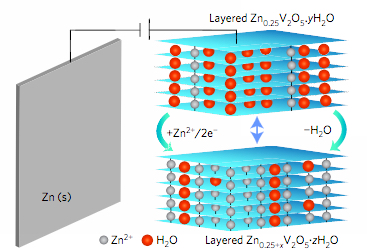
The zinc-ion battery consists of a water-based electrolyte, a pillared vanadium oxide positive electrode (right), and an inexpensive metallic zinc negative electrode (left). The battery generates electricity through a reversible process called intercalation, where positively-charged zinc ions are oxidized from the zinc metal negative electrode, travel through the electrolyte and insert between the layers of vanadium oxide nanosheets in the positive electrode. This drives the flow of electrons in the external circuit, creating an electrical current. The reverse process occurs on charge. (credit: Dipan Kundu et al./Nature Energy)

University of Waterloo chemists have developed a long-lasting, safe, zinc-ion battery that costs half the price of current lithium-ion batteries. It could help communities shift from traditional power plants to renewable solar and wind energy production, where electricity storage overnight is needed.

The battery is water-based and uses cheap but safe, non-flammable, non-toxic materials, compared to expensive, flammable, organic electrolytes in lithium-ion batteries, which are used in the exploding Samsung Galaxy Note 7 smartphones reported last week and in previously reported exploding hoverboards.

Where cost, safety, and life cycle are vital, not size

Lithium-ion batteries have much higher energy density (energy that can be stored per unit volume) than water-based batteries (making lithium-ion batteries attractive for smartphones and other compact devices), but water-based zinc-ion batteries are more feasible for grid-scale applications, where cost, safety, and life cycle are important, not size.

The cell design satisfies four vital criteria: high reversibility, rate, capacity, and no zinc dendrite formation. It provides more than 1,000 cycles. Lithium-ion batteries also operate by intercalation (of lithium ions) but they typically use expensive, flammable, organic electrolytes.

The bonus for manufacturers is they can produce this zinc battery at low cost because its fabrication does not require special conditions, such as ultra-low humidity or the handling of flammable materials needed for lithium ion batteries, the chemists say.

“The focus used to be on minimizing size and weight for the portable electronics market and cars,” said Dipan Kundu, a University of Waterloo postdoctoral fellow and the paper’s first author. “Grid storage needs a different kind of battery and that’s given us license to look into different materials.”

The discovery appears in the journal Nature Energy.


Abstract of A high-capacity and long-life aqueous rechargeable zinc battery using a metal oxide intercalation cathode

Although non-aqueous Li-ion batteries possess significantly higher energy density than their aqueous counterparts, the latter can be more feasible for grid-scale applications when cost, safety and cycle life are taken into consideration. Moreover, aqueous Zn-ion batteries have an energy storage advantage over alkali-based batteries as they can employ Zn metal as the negative electrode, dramatically increasing energy density. However, their development is plagued by a limited choice of positive electrodes, which often show poor rate capability and inadequate cycle life. Here we report a vanadium oxide bronze pillared by interlayer Zn2+ ions and water (Zn0.25V2O5nH2O), as the positive electrode for a Zn cell. A reversible Zn2+ ion (de)intercalation storage process at fast rates, with more than one Zn2+ per formula unit (a capacity up to 300 mAh g−1), is characterized. The Zn cell offers an energy density of ∼450 Wh l−1 and exhibits a capacity retention of more than 80% over 1,000 cycles, with no dendrite formation at the Zn electrode.