Why partially automated cars should be deployed in ‘light-duty vehicles’

Crash avoidance technologies now available in non-luxury vehicles include Lane Departure Warning (LDW), Forward Collision Warning (FCW), and Blind Spot Monitoring Roadway (BSM). (credit: Corey D. Harper et al./Accident Analysis and Prevention)

U.S. National Highway Traffic Safety Administration chief Mark Rosekind said at a conference today (July 20) that the government “will not abandon efforts to speed the development of self-driving cars … to reduce the 94 percent of car crashes attributed to human error, despite a fatal accident involving a Tesla Model S operating on an autopilot system,” Reuters reports. But autonomous vehicles must be “much safer” than human drivers before they are deployed on U.S. roads, he added.

However, Carnegie Mellon College of Engineering researchers suggest that already-available partially automated vehicle crash-avoidance technologies are a practical interim solution, they conclude in a study published in the journal Accident Analysis and Prevention.

These technologies — which include forward collision warning and avoidance, lane departure warning, blind spot monitoring, and partially autonomous braking or controls — are already available in non-luxury vehicles such as the Honda Accord and Mazda CX-9. If these technologies were deployed in all “light-duty vehicles,” it could prevent or reduce the severity of up 1.3 million crashes a year, including 10,100 fatal wrecks, according to the study.

“While there is much discussion about driverless vehicles, we have demonstrated that even with partial automation, there are financial and safety benefits,” says Chris T. Hendrickson, director of the Carnegie Mellon Traffic21 Institute.

When the team compared the price of equipping cars with safety technology to the expected annual reduction in the costs of crashes (based on government and insurance industry data), they discovered a net cost benefit (in addition to life-saving benefits) in two scenarios:

  • In the perfect-world scenario in which all relevant crashes are avoided with these technologies, there is an annual benefit of $202 billion or $861 per car.
  • On the more conservative side, when only observed crash reductions in vehicles equipped with blind spot monitoring, lane departure and forward collision crash avoidance systems are considered, there is still an annual positive net benefit of $4 billion dollars or $20 a vehicle (and lower prices could lead to larger net benefits over time).

Carnegie Mellon’s Technologies for Safe and Efficient Transportation (T-SET) University Transportation Center, the National Science Foundation, and the Hillman Foundation funded the project.


Abstract of Cost and benefit estimates of partially-automated vehicle collision avoidance technologies

Many light-duty vehicle crashes occur due to human error and distracted driving. Partially-automated crash avoidance features offer the potential to reduce the frequency and severity of vehicle crashes that occur due to distracted driving and/or human error by assisting in maintaining control of the vehicle or issuing alerts if a potentially dangerous situation is detected. This paper evaluates the benefits and costs of fleet-wide deployment of blind spot monitoring, lane departure warning, and forward collision warning crash avoidance systems within the US light-duty vehicle fleet. The three crash avoidance technologies could collectively prevent or reduce the severity of as many as 1.3 million U.S. crashes a year including 133,000 injury crashes and 10,100 fatal crashes. For this paper we made two estimates of potential benefits in the United States: (1) the upper bound fleet-wide technology diffusion benefits by assuming all relevant crashes are avoided and (2) the lower bound fleet-wide benefits of the three technologies based on observed insurance data. The latter represents a lower bound as technology is improved over time and cost reduced with scale economies and technology improvement. All three technologies could collectively provide a lower bound annual benefit of about $18 billion if equipped on all light-duty vehicles. With 2015 pricing of safety options, the total annual costs to equip all light-duty vehicles with the three technologies would be about $13 billion, resulting in an annual net benefit of about $4 billion or a $20 per vehicle net benefit. By assuming all relevant crashes are avoided, the total upper bound annual net benefit from all three technologies combined is about $202 billion or an $861 per vehicle net benefit, at current technology costs. The technologies we are exploring in this paper represent an early form of vehicle automation and a positive net benefit suggests the fleet-wide adoption of these technologies would be beneficial from an economic and social perspective.

Peering into atomically thin transistors with microwaves, scientists make a radical discovery: a one-dimensional transistor

Peering into an atomically thin semiconductor device with a “microwave microscope” via an AFM tip (credit: University of Texas at Austin)

Physicists at The University of Texas at Austin have had the first-ever glimpse into what happens inside an atomically thin semiconductor device. In doing so, they discovered that a transistor may be possible within a space so small (the edge) that it’s effectively one-dimensional.

Future tech innovations will require finding a way to fit more transistors on computer chips to keep up with Moore’s law, so experts have begun exploring new semiconducting materials, including one called molybdenum disulfide (MoS2), as KurzweilAI reported last week. In a paper published July 18 in the Proceedings of the National Academy of Sciencesthe researchers describe seeing the detailed inner workings of this new type of two-dimensional transistor.

Unlike today’s silicon-based devices, transistors made from MoS2 allow for on-off signaling on a single 2-D (flat) plane.

Computing on a one-dimensional edge

Keji Lai*, an assistant professor of physics, and his team used a “microwave impedance microscope” that he invented and that pointed microwaves at the 2-D device. Using an atomic force microscope (AFM) tip only 100 nanometers wide, the microwave microscope allowed the scientists to see conductivity changes inside the transistor for the first time.

That’s when they discovered that with MoS2, the conductive signaling happens much differently than with silicon — in a way that could promote future energy savings in devices.

With silicon transistors, the entire device is either turned on or off. With 2-D transistors, by contrast, Lai and the team found that electric currents move in a more phased (or wave-like) way, beginning first at the edges before appearing in the interior. Lai says this suggests the same current could be sent with less power and in an even tinier space — using a one-dimensional edge (a line) instead of the two-dimensional plane (area).

“In physics, edge states often carry a lot of interesting phenomena, and here, they are the first to turn on. In the future, if we can engineer this material very carefully, then these edges can carry the full current,” Lai says. “We don’t really need the entire thing, because the interior is useless. Just having the edges running to get a current working would substantially reduce the power loss.”

Eliminating defects

Researchers have been working to get a view into what happens inside a 2-D transistor for years to better understand both the potential and the limitations of the new materials. Getting 2-D transistors ready for commercial devices, such as paper-thin computers and cellphones, is expected to take several more years. Lai says scientists need more information about what interferes with performance in devices made from the new materials.

Besides seeing the currents’ motion, the scientists found thread-like defects in the middle of the transistors. Lai says this suggests the new material will need to be made cleaner to function optimally. “If we could make the material clean enough, the edges will be carrying even more current, and the interior won’t have as many defects,” Lai says.

The research was supported by the U.S. Department of Energy, the Welch Foundation, the Office of Naval Research, and the National Science Foundation.

* Earlier this year, Lai and co-researcher Deji Akinwande, associate professor of UT Austin’s Department of Electrical and Computer Engineering, won Presidential Early Career Awards for Scientists and Engineers, the U.S. government’s highest honor for early-stage scientists and engineers.


UT | In this visualization of what happens inside a 2-D transistor made of a promising new material called MoS2, electric currents appear initially at the outer edges and then inside of the device. Thread-like flaws can be seen in the interior part of the transistor.


Abstract of Uncovering edge states and electrical inhomogeneity in MoS2 field-effect transistors

The understanding of various types of disorders in atomically thin transition metal dichalcogenides (TMDs), including dangling bonds at the edges, chalcogen deficiencies in the bulk, and charges in the substrate, is of fundamental importance for TMD applications in electronics and photonics. Because of the imperfections, electrons moving on these 2D crystals experience a spatially nonuniform Coulomb environment, whose effect on the charge transport has not been microscopically studied. Here, we report the mesoscopic conductance mapping in monolayer and few-layer MoS2 field-effect transistors by microwave impedance microscopy (MIM). The spatial evolution of the insulator-to-metal transition is clearly resolved. Interestingly, as the transistors are gradually turned on, electrical conduction emerges initially at the edges before appearing in the bulk of MoS2 flakes, which can be explained by our firstprinciples calculations. The results unambiguously confirm that the contribution of edge states to the channel conductance is significant under the threshold voltage but negligible once the bulk of the TMD device becomes conductive. Strong conductance inhomogeneity, which is associated with the fluctuations of disorder potential in the 2D sheets, is also observed in the MIM images, providing a guideline for future improvement of the device performance.

World’s smallest storage device writes information atom by atom

STM scan (96 nm wide, 126 nm tall) of the 1 kB memory, written to a section of Feynman’s lecture, “There’s Plenty of Room at the Bottom” (credit: TU Delft/Ottelab)

Scientists at Kavli Institute of Nanoscience at Delft University have built a nanoscale data storage device containing 1 kilobyte (8,000 bits) with a storage density of 500 terabits per square inch (Tbpsi) — 500 times denser than the best commercial hard disk drive currently available. Each bit is represented by the position of one single chlorine atom.

“In theory, this storage density would allow all books ever created by humans to be written on a single post stamp,” says lead scientist Sander Otte. The research is reported today (Monday July 18) in Nature Nanotechnology.

Every day, modern society creates more than a billion gigabytes of new data. To store all this data, it is increasingly important that each single bit occupies as little space as possible.

In 1959, physicist Richard Feynman challenged his colleagues to engineer the world at the smallest possible scale. In his famous lecture There’s Plenty of Room at the Bottom, he speculated that if we had a platform allowing us to arrange individual atoms in an exact orderly pattern, it would be possible to store one piece of information per atom. To honor the visionary Feynman, Otte and his team have coded a section of Feynman’s lecture on an area 100 nanometers wide.

“Sliding puzzle” scheme

Atomic data storage scheme (credit: Kavli Institute of Nanoscience)

The team used a scanning tunneling microscope (STM), in which a sharp needle probes the atoms of a surface, one by one. With these probes scientists can see atoms and push them around. “You could compare it  to a sliding puzzle,” Otte explains. “Every bit consists of two positions on a surface of copper atoms, and one chlorine atom that we can slide back and forth between these two positions. If the chlorine atom is in the top position, there is a hole beneath it — we call this a 1. If the hole is in the top position and the chlorine atom is therefore on the bottom, then the bit is a 0.”

Because the chlorine atoms are surrounded by other chlorine atoms, except near the holes, they keep each other in place. Which is why this method with holes is much more stable than methods with loose atoms and more suitable for data storage.

Kilobyte atomic memory. 1,016-byte atomic memory, written to a passage from Feynman’s lecture, “There’s plenty of room at the bottom.” The memory consists of 127 functional blocks and 17 broken blocks, resulting in an overall areal density of 0.778 bits per nm square. (credit: F. E. Kalff et al./Nature Nanotechnology)

The researchers organized their memory in blocks of 8 bytes (64 bits). Each block has a marker, made of the same type of “holes” as the raster of chlorine atoms. Inspired by the pixelated square barcodes (QR codes) often used to scan tickets for airplanes and concerts, these markers work like miniature QR codes that carry information about the precise location of the block on the copper layer. The code will also indicate if a block is damaged, for instance due to some local contaminant or an error in the surface. This allows the memory to be scaled up easily to very big sizes, even if the copper surface is not entirely perfect.

The new approach offers excellent prospects in terms of stability and scalability. However, “in its current form the memory can operate only in very clean vacuum conditions and at liquid nitrogen temperature (77 K), so the actual storage of data on an atomic scale is still some way off.”

This research was support by the Netherlands Organisation for Scientific Research (NOW/FOM). Scientists of the International Iberian Nanotechnology Laboratory (INL) in Portugal performed calculations on the behavior of the chlorine atoms.


Delft University of Technology | Atomic scale data storage


Abstract of A kilobyte rewritable atomic memory

The advent of devices based on single dopants, such as the single-atom transistor, the single-spin magnetometer and the single-atom memory, has motivated the quest for strategies that permit the control of matter with atomic precision. Manipulation of individual atoms by low-temperature scanning tunnelling microscopy provides ways to store data in atoms, encoded either into their charge state, magnetization state or lattice position. A clear challenge now is the controlled integration of these individual functional atoms into extended, scalable atomic circuits. Here, we present a robust digital atomic-scale memory of up to 1 kilobyte (8,000 bits) using an array of individual surface vacancies in a chlorine-terminated Cu(100) surface. The memory can be read and rewritten automatically by means of atomic-scale markers and offers an areal density of 502 terabits per square inch, outperforming state-of-the-art hard disk drives by three orders of magnitude. Furthermore, the chlorine vacancies are found to be stable at temperatures up to 77 K, offering the potential for expanding large-scale atomic assembly towards ambient conditions.

DNA origami creates a microscopic glowing Van Gogh

This reproduction of van Gogh’s The Starry Night contains 65,536 glowing pixels but is just the width of a dime across, as a proof-of-concept of precision placement of DNA origami (credit: Paul Rothemund and Ashwin Gopinath/Caltech)

Using folded DNA to precisely place glowing molecules within microscopic light resonators, researchers at Caltech have created one of the world’s smallest reproductions of Vincent van Gogh’s The Starry Night. The feat is a proof-of-concept of how precision placement of DNA origami can be used to build hybrid nanophotonic devices at smaller scales than ever before.

DNA origami, developed 10 years ago by Caltech’s research professor Paul Rothemund, is a technique that allows researchers to fold (in a test tube) a long strand of self-assembling DNA into any desired shape. The folded DNA then acts as a scaffold (support) onto which researchers can attach nanometer-scale components. KurzweilAI has reported extensively on DNA origami — most recently, an automated design method for creating nanoparticles for drug delivery and cell targeting, nanoscale robots, custom-tailored optical devices, and DNA as a data storage medium, for example.

Meanwhile, over the last seven years, Rothemund and associates have refined and extended DNA orgami so that DNA shapes can be precisely positioned on almost any surface used in the manufacture of computer chips. Now, in a Nature paper on July 11, they report the first application of the technique — using DNA origami to install fluorescent molecules into microscopic light sources for use in single-molecule detection, quantum computers, and other applications.

The work was supported by the Army Research Office, the Office of Naval Research, the Air Force Office of Scientific Research, and the National Science Foundation.


Abstract of Engineering and mapping nanocavity emission via precision placement of DNA origami

Many hybrid devices integrate functional molecular or nanoparticle components with microstructures, as exemplified by the nanophotonic devices that couple emitters to optical resonators for potential use in single-molecule detection, precision magnetometry, low threshold lasing and quantum information processing. These systems also illustrate a common difficulty for hybrid devices: although many proof-of-principle devices exist, practical applications face the challenge of how to incorporate large numbers of chemically diverse functional components into microfabricated resonators at precise locations. Here we show that the directed self-assembly of DNA origami onto lithographically patterned binding sites allows reliable and controllable coupling of molecular emitters to photonic crystal cavities (PCCs). The precision of this method is sufficient to enable us to visualize the local density of states within PCCs by simple wide-field microscopy and to resolve the antinodes of the cavity mode at a resolution of about one-tenth of a wavelength. By simply changing the number of binding sites, we program the delivery of up to seven DNA origami onto distinct antinodes within a single cavity and thereby digitally vary the intensity of the cavity emission. To demonstrate the scalability of our technique, we fabricate 65,536 independently programmed PCCs on a single chip. These features, in combination with the widely used modularity of DNA origami, suggest that our method is well suited for the rapid prototyping of a broad array of hybrid nanophotonic devices.

Berkeley Lab scientists grow atomically thin transistors and circuits

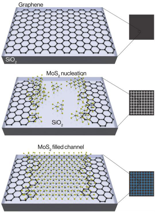
This schematic shows the chemical assembly of two-dimensional crystals. Graphene is first etched into channels and the TMDC molybdenum disulfide (MoS2) begins to nucleate around the edges and within the channel. On the edges, MoS2 slightly overlaps on top of the graphene. Finally, further growth results in MoS2 completely filling the channels. (credit: Berkeley Lab)

In an advance that helps pave the way for next-generation electronics and computing technologies — and possibly paper-thin devices — scientists with the U.S. Department of Energy’s Lawrence Berkeley National Laboratory (Berkeley Lab) have developed a way to chemically assemble transistors and circuits that are only a few atoms thick.

In addition, their method yields functional structures at a scale large enough to begin thinking about real-world applications and commercial scalability.

They reported their research online July 11 in the journal Nature Nanotechnology.

The scientists controlled the synthesis of a transistor in which narrow channels were etched onto conducting graphene, and a semiconducting material called a transition-metal dichalcogenide (TMDC) was seeded in the blank channels.

Both of these materials are single-layered crystals and atomically thin, so the two-part assembly yielded electronic structures that are essentially two-dimensional, and cover an area a few centimeters long and a few millimeters wide.

“This is a big step toward a scalable and repeatable way to build atomically thin electronics or pack more computing power in a smaller area,” says Xiang Zhang, a senior scientist in Berkeley Lab’s Materials Sciences Division who led the study.

Their work is part of a new wave of research aimed at keeping pace with Moore’s Law, which holds that the number of transistors in an integrated circuit doubles approximately every two years. To keep this pace, scientists predict that integrated electronics will soon require transistors that measure less than ten nanometers in length.

“With silicon, this will be extremely challenging, because the thickness of the transistor’s channel will become greater than the channel length, ultimately leading to difficult electrostatic control via the transistor gate,” the authors note. Nanomaterials such as inorganic nanowires and Stanford/IBM’s carbon nanotubes have been proposed, but require impractical “precise placement and orientation using complex fabrication techniques,” the authors point out.

The two-dimensional solution for keeping up with Moore’s law

Optical image of the atomically thin graphene–MoS heterostructure. Arrows indicate nucleation (junctions) with graphene of the MoS2 areas, forming transistors. (credit: Mervin Zhao et al./Nature Nanotechnology)

So researchers have now looked to two-dimensional crystals that are only one molecule thick as alternative materials to keep up with Moore’s Law. Using that approach, the Berkeley Lab scientists developed a way to seed a single-layered semiconductor — in this case, the TMDC molybdenum disulfide (MoS2) — into channels lithographically etched within a sheet of conducting graphene. The two atomic sheets meet to form nanometer-scale junctions that make atomically thin transistors in which the graphene conductor efficiently injects current into the MoS2.

“This approach allows for the chemical assembly of electronic circuits, using two-dimensional materials, which show improved performance compared to using traditional metals to inject current into TMDCs,” says Mervin Zhao, a lead author and Ph.D. student in Zhang’s group at Berkeley Lab and UC Berkeley.

The scientists demonstrated the usefulness of the structure by assembling it into the logic circuitry of an inverter (NOT gate). This further underscores the technology’s ability to lay the foundation for a chemically assembled atomic computer, the scientists say. They also note that the two-dimensional crystals were synthesized at a wafer scale, so the scalable design is compatible with current semiconductor manufacturing.

The research was supported by the Office of Naval Research and the National Science Foundation. Scientists from Cornell University were also involved in the research.


Abstract of Large-scale chemical assembly of atomically thin transistors and circuits

Next-generation electronics calls for new materials beyond silicon, aiming at increased functionality, performance and scaling in integrated circuits. In this respect, two-dimensional gapless graphene and semiconducting transition-metal dichalcogenides have emerged as promising candidates due to their atomic thickness and chemical stability. However, difficulties with precise spatial control during their assembly currently impede actual integration into devices. Here, we report on the large-scale, spatially controlled synthesis of heterostructures made of single-layer semiconducting molybdenum disulfide contacting conductive graphene. Transmission electron microscopy studies reveal that the single-layer molybdenum disulfide nucleates at the graphene edges. We demonstrate that such chemically assembled atomic transistors exhibit high transconductance (10 µS), on–off ratio (∼106) and mobility (∼17 cm2 V−1 s−1). The precise site selectivity from atomically thin conducting and semiconducting crystals enables us to exploit these heterostructures to assemble two-dimensional logic circuits, such as an NMOS inverter with high voltage gain (up to 70).

Locusts engineered as biorobotic sensing machines

Sensors placed on the insect monitor neural activity while they are freely moving, decoding the odorants present in their environment. (credit: Baranidharan Raman)

Washington University in St. Louis engineers have developed an innovatiave “bio-hybrid nose” that could be used in homeland security applications, such as detecting explosives, replacing state-of-the-art miniaturized chemical sensing devices limited to a handful of sensors.

Compare that to the locust antenna (where their chemical sensors are located): “it has several hundreds of thousands of sensors and of a variety of types,” says Baranidharan Raman, associate professor of biomedical engineering, who has received a three-year, $750,000 grant from the Office of Naval Research (ONR).

The team previously found that locusts can correctly identify a particular odor, even with other odors present — and even in complex situations, such as overlapping with other scents or in different background conditions.

Replacing canines

In previous research, the opening of the locust maxillary palps to the trained odorant was used as an indicator of acquired memory. The palps were painted with non-odorous organic-chemical green paint to facilitate tracking. (credit: Debajit Saha et al./Nature Communications)

The ingenious idea in the new study by the Raman Lab is to remotely monitor neural activity from the insect brain while they are freely moving, exploring, and decoding the odorants present in their environment, which will require innovative low-power electronic components to collect, log, and transmit data.

The locusts could also collect samples using remote control. To do that, the engineers are developing a plasmonic “tattoo” made of a biocompatible silk to apply to the locusts’ wings. It will generate mild heat to help steer locusts to move toward particular locations by remote control. The tattoos, studded with plasmonic nanostructures, also can collect samples of volatile organic compounds in their proximity, which would allow the researchers to conduct secondary analysis of the chemical makeup of the compounds using more conventional methods.

“The canine olfactory system still remains the state-of-the-art sensing system for many engineering applications, including homeland security and medical diagnosis,” Raman said. “However, the difficulty and the time necessary to train and condition these animals, combined with lack of robust decoding procedures to extract the relevant chemical sending information from the biological systems, pose a significant challenge for wider application.

New tech could have helped police locate shooters in Dallas

Potential shooter location in Dallas (credit: Fox News)

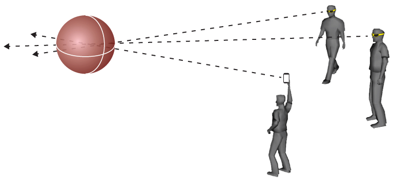
JULY 8, 3:56 AM EDT — Livestreamed data from multiple users with cell phones and other devices could be used to help police locate shooters in a situation like the one going on right now in Dallas, says Jon Fisher, CEO of San Francisco-based CrowdOptic.

Here’s how it would work: You view (or record a video of) a shooter with your phone. Your location and the direction you are facing is now immediately available on your device and could be coordinated with data from other persons at the scene to triangulate the position of the shooter.

A CrowdOptic “cluster” with multiple people focused on the same object (credit: CrowdOptic)

This technology, called the “CrowdOptic Interactive Streaming platform,” is already in place, using Google Glass livestreaming, in several organizations, including UCSF Medical Center, Denver Broncos, and Futton, Inc. (working with Chinese traffic police).

Fisher told KurzweilAI his company’s software is also integrated with Cisco Jabber livestreaming video and conferencing products (and soon Spark), and with Sony SmartEyeglass, and that iOS and Android apps are planned.

CrowdOptic also has a product called CrowdOptic Eye, a “powerful, low-bandwidth live streaming device designed to … broadcast live video and two-way audio from virtually anywhere.”

“We’re talking about phones now, but think about all other devices, such as drones, that will be delivering these feeds to CNN and possibly local police,” he said.

ADDED July 11:

“When all attempts to negotiate with the suspect, Micah Johnson, failed under the exchange of gunfire, the Department utilized the mechanical tactical robot, as a last resort, to deliver an explosion device to save the lives of officers and citizens. The robot used was the Remotec, Model  F-5, claw and arm extension with an explosive device of C4 plus ‘Det’ cord.  Approximate weight of total charge was one pound.” — Statement July 9, 2016 by Dallas police chief David O. Brown

The Dallas police department’s decision to use a robot to kill the shooter Thursday July 7, raises questions. For example: Why wasn’t a non-lethal method used with the robot, such as a tranquilizer dart, which also might have given police an opportunity to acquire more information, including the location of claimed bombs and cohorts possibly associated with the crime?

AI beats top U.S. Air Force tactical air combat experts in combat simulation

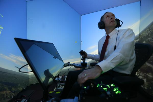
Retired U.S. Air Force Colonel Gene Lee, in a flight simulator, takes part in simulated air combat versus artificial intelligence technology developed by a team from industry, the U.S. Air Force, and University of Cincinnati. (credit: Lisa Ventre, University of Cincinnati Distribution A: Approved for public release; distribution unlimited. 88ABW Cleared 05/02/2016; 88ABW-2016-2270)

The U.S. Air Force got a wakeup call recently when AI software called ALPHA — running on a tiny $35 Raspberry Pi computer — repeatedly defeated retired U.S. Air Force Colonel Gene Lee, a top aerial combat instructor and Air Battle Manager, and other expert air-combat tacticians at the U.S. Air Force Research Lab (AFRL) in Dayton, Ohio. The contest was conducted in a high-fidelity air combat simulator.

According to Lee, who has considerable fighter-aircraft expertise (and has been flying in simulators against AI opponents since the early 1980s), ALPHA is “the most aggressive, responsive, dynamic and credible AI I’ve seen to date.” In fact, he was shot out of the air every time during protracted engagements in the simulator, he said.

ALPHA’s secret? Custom-designed “genetic fuzzy” algorithms designed for simulated air-combat missions, according to an open-access, unclassified paper published in the authoritative Journal of Defense Management. The paper was authored by a team of industry, Air Force, and University of Cincinnati researchers, including the AFRL Branch Chief.

ALPHA, which now runs on a standard consumer-grade PC, was developed by Psibernetix, Inc., an AFRL contractor founded by University of Cincinnati College of Engineering and Applied Science 2015 doctoral graduate Nick Ernest*, president and CEO of the firm, and a team of former Air Force aerial combat experts, including Lee.

“AI wingmen”

Today’s fighters close in on each other at speeds in excess of 1,500 miles per hour while flying at altitudes above 40,000 feet. The cost for a mistake is very high. Microseconds matter, but an average human visual reaction time is 0.15 to 0.30 seconds, and “an even longer time to think of optimal plans and coordinate them with friendly forces,” the researchers note in the paper.

Side view during active combat in simulator between two Blue (human-controlled) fighters vs. four Red (AI) fighters with >150 inputs but handicapped data sources. All Reds have successfully evaded missiles; one Blue has been destroyed. Blue AWACS [Airborne early warning and control system aircraft] shown in distance. (credit: Nicholas Ernest et al./Journal of Defense Management)

In fact, ALPHA works 250 times faster than humans, the researchers say. Nonetheless, ALPHA’s future role will stop short of fully autonomous combat.

According to the AFRL team, ALPHA will first be tested on “Unmanned Combat Aerial Vehicles (UCAV),” where ALPHA will be organizing data and creating a complete mapping of a combat scenario, such as a flight of four fighter aircraft — which it can do in less than a millisecond.

The AFRL team sees ACAVs as “AI wingmen” capable of engaging in air combat when teamed with manned aircraft.

The ACAVs will include an onboard battle management system able to process situational awareness, determine reactions, select tactics, and manage weapons — simultaneously evading dozens of hostile missiles, taking accurate shots at multiple targets, coordinating actions of squad mates, and recording and learning from observations of enemy tactics and capabilities.

Genetic fuzzy systems

The researchers based the design of ALPHA on a “genetic fuzzy tree” (GFT) — a subtype of “fuzzy logic” algorithms. The GFT is described in another open-access paper in Journal of Defense Management by Ernest and University of Cincinnati aerospace professor Kelly Cohen.

“Genetic fuzzy systems have been shown to have high performance, and a problem with four or five inputs can be solved handily,” said Cohen. “However, boost that to a hundred inputs, and no computing system on planet Earth could currently solve the processing challenge involved — unless that challenge and all those inputs are broken down into a cascade of sub-decisions.

“Most AI programming uses numeric-based control and provides very precise parameters for operations,” he said. In contrast, the AI algorithms that Ernest and his team developed are language-based, with if/then scenarios and rules able to encompass hundreds to thousands of variables. This language-based control, or fuzzy logic, can be verified and validated, Cohen says.

The “genetic” part of the “genetic fuzzy tree” system started with numerous automatically generated versions of ALPHA that proved themselves against a manually tuned version of ALPHA. The successful strings of code were then “bred” with each other, favoring the stronger, or highest performance versions.

In other words, only the best-performing code was used in subsequent generations. Eventually, one version of ALPHA rises to the top in terms of performance, and that’s the one that is utilized.

“In terms of emulating human reasoning, I feel this is to unmanned aerial vehicles as the IBM Deep Blue vs. Kasparov was to chess,” said Cohen. Or as Alpha Go was to Go.

* Support for Ernest’s doctoral research was provided  by the Dayton Area Graduate Studies Institute and the U.S. Air Force Research Laboratory.


UC | Flying in Simulator


Abstract of Genetic Fuzzy based Artificial Intelligence for Unmanned Combat Aerial Vehicle Control in Simulated Air Combat Missions

Breakthroughs in genetic fuzzy systems, most notably the development of the Genetic Fuzzy Tree methodology, have allowed fuzzy logic based Artificial Intelligences to be developed that can be applied to incredibly complex problems. The ability to have extreme performance and computational efficiency as well as to be robust to uncertainties and randomness, adaptable to changing scenarios, verified and validated to follow safety specifications and operating doctrines via formal methods, and easily designed and implemented are just some of the strengths that this type of control brings. Within this white paper, the authors introduce ALPHA, an Artificial Intelligence that controls flights of Unmanned Combat Aerial Vehicles in aerial combat missions within an extreme-fidelity simulation environment. To this day, this represents the most complex application of a fuzzy-logic based Artificial Intelligence to an Unmanned Combat Aerial Vehicle control problem. While development is on-going, the version of ALPHA presented within was assessed by Colonel (retired) Gene Lee who described ALPHA as “the most aggressive, responsive, dynamic and credible AI (he’s) seen-to-date.” The quality of these preliminary results in a problem that is not only complex and rife with uncertainties but also contains an intelligent and unrestricted hostile force has significant implications for this type of Artificial Intelligence. This work adds immensely to the body of evidence that this methodology is an ideal solution to a very wide array of problems.

A smarter ‘bionic’ cardiac patch that doubles as advanced pacemaker/arrhythmia detector

(a) Schematic of the free-standing macroporous nanoelectronic scaffold with nanowire FET (field effect transistor) arrays (red dots). Inset: one nanowire FET. (b) Folded 3D free-standing scaffolds with four layers of individually addressable FET sensors. (c) Schematic of nanoelectronic scaffold/cardiac tissue resulting from the culturing of cardiac cells within the 3D folded scaffold. Inset: the nanoelectronic sensors (blue circles) innervate the 3D cell network. (credit: Xiaochuan Dai at al./Nature Nanotechnology)

Harvard researchers have designed nanoscale electronic scaffolds (support structures) that can be seeded with cardiac cells to produce a new “bionic” cardiac patch (for replacing damaged cardiac tissue with pre-formed tissue patches). It also functions as a more sophisticated pacemaker: In addition to electrically stimulating the heart, the new design can change the pacemaker stimulation frequency and direction of signal propagation.

In addition, because because its electronic components are integrated throughout the tissue (instead of being located on the surface of the skin), it could detect arrhythmia far sooner, and “operate at far lower (safer) voltages than a normal pacemaker, [which] because it’s on the surface, has to use relatively high voltages,” according to Charles Lieber, the Mark Hyman, Jr. Professor of Chemistry and Chair of the Department of Chemistry and Chemical Biology.

Early arrhythmia detection, monitoring responses to cardiac drugs

“Even before a person started to go into large-scale arrhythmia that frequently causes irreversible damage or other heart problems, this could detect the early-stage instabilities and intervene sooner,” he said. “It can also continuously monitor the feedback from the tissue and actively respond.”

The patch might also find use, Lieber said, as a tool to monitor responses to cardiac drugs, or to help pharmaceutical companies screen the effectiveness of drugs under development.

In the long term, Lieber believes, the development of nanoscale tissue scaffolds represents a new paradigm for integrating biology with electronics in a virtually seamless way.

The bionic cardiac patch can also be a unique platform to study the tissue behavior evolving during some developmental processes, such as aging, ischemia, or differentiation of stem cells into mature cardiac cells.

Although the bionic cardiac patch has not yet been implanted in animals, “we are interested in identifying collaborators already investigating cardiac patch implantation to treat myocardial infarction in a rodent model,” he said. “I don’t think it would be difficult to build this into a simpler, easily implantable system.”

Could one day deliver cardiac patch/pacemaker via injection

Using the injectable electronics technology he pioneered last year, Lieber even suggested that similar cardiac patches might one day simply be delivered by injection. “It may actually be that, in the future, this won’t be done with a surgical patch,” he said. “We could simply do a co-injection of cells with the mesh, and it assembles itself inside the body, so it’s less invasive.”

“I think one of the biggest impacts would ultimately be in the area that involves replacement of damaged cardiac tissue with pre-formed tissue patches,” Lieber said. “Rather than simply implanting an engineered patch built on a passive scaffold, our work suggests it will be possible to surgically implant an innervated patch that would now be able to monitor and subtly adjust its performance.”

In the long term, Lieber believes, the development of nanoscale tissue scaffolds represents a new paradigm for integrating biology with electronics in a virtually seamless way.

The study is described in a June 27 paper published in Nature Nanotechnology.


Abstract of Three-dimensional mapping and regulation of action potential propagation in nanoelectronics-innervated tissues

Real-time mapping and manipulation of electrophysiology in three-dimensional (3D) tissues could have important impacts on fundamental scientific and clinical studies, yet realization is hampered by a lack of effective methods. Here we introduce tissue-scaffold-mimicking 3D nanoelectronic arrays consisting of 64 addressable devices with subcellular dimensions and a submillisecond temporal resolution. Real-time extracellular action potential (AP) recordings reveal quantitative maps of AP propagation in 3D cardiac tissues, enable in situtracing of the evolving topology of 3D conducting pathways in developing cardiac tissues and probe the dynamics of AP conduction characteristics in a transient arrhythmia disease model and subsequent tissue self-adaptation. We further demonstrate simultaneous multisite stimulation and mapping to actively manipulate the frequency and direction of AP propagation. These results establish new methodologies for 3D spatiotemporal tissue recording and control, and demonstrate the potential to impact regenerative medicine, pharmacology and electronic therapeutics.

Artificial synapse said to rival biological synapses in energy consumption and function

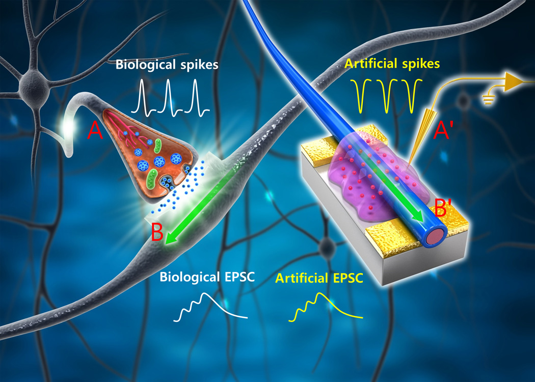
Schematic of biological neuronal network and an organic nanowire (ONW) synaptic transistor (ST) that emulates a biological synapse. The yellow conductive lines and probe (A′) mimic an axon (A) that delivers presynaptic spikes from a pre-neuron to the presynaptic membrane. The mobile ions in the ion gel move in the electrical field, analogous to the biological neuron transmitters in the synaptic cleft; the field later induces an excitatory postsynaptic current (EPSC, light blue line) in the biological dendrite (B). An ONW (B′) combined with a drain electrode (yellow surface) mimics a biological dendrite (B). EPSC (light green line) is generated in the ONW in response to presynaptic spikes and is delivered to a post-neuron through connections to the drain electrode. (credit: Wentao Xu et al./Science Advances)

An artificial synapse that emulates a biological synapse while requiring less energy has been developed by Pohang University Of Science & Technology (POSTECH) researchers* in Korea.

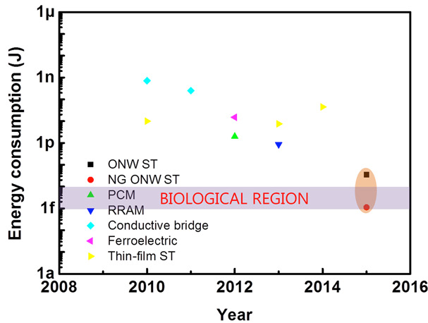
Energy consumption in Joules per synaptic event of currently available synaptic devices.*** NG, nanogap; PCM, phase change memory; RRAM, resistive switching random access memory. (credit: Wentao Xu et al./Science Advances)

A human synapse consumes an extremely small amount of energy (~10 fJ or femtojoules** per synaptic event).

The researchers have fabricated an organic nanofiber (ONF), or organic nanowire (ONW), electronic device that emulates the important working principles and energy consumption of biological synapses while requiring only ~1 fJ per synaptic event. The ONW also emulates the morphology (form) of a synapse.

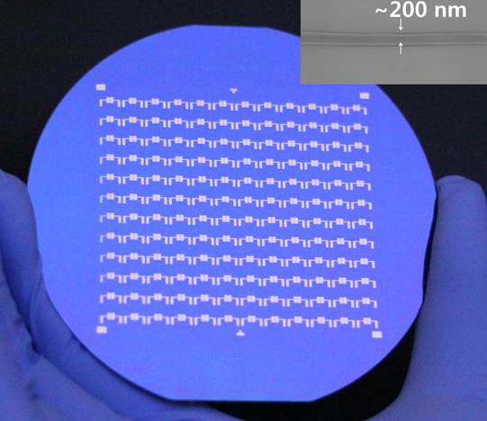
Array of 144 ONW STs (organic nanowire synaptic transistors) fabricated on a 4-inch silicon wafer. Inset: Scanning electron microscopy (SEM) image of a typical ONW with a diameter of 200 nm. (credit: Wentao Xu et al./Science Advances)

The morphology of ONFs is similar to that of nerve fibers, which form crisscrossing grids to enable the high memory density of a human brain. The researchers say the highly-aligned ONFs can be massively produced with precise control over alignment and dimension; and this morphology may make possible the future construction of the high-density memory of a neuromorphic (brain-form-emulating) system.****

The researchers say they have emulated important working principles of a biological synapse, such as paired-pulse facilitation (PPF), short-term plasticity (STP), long-term plasticity (LTP), spike-timing dependent plasticity (STDP), and spike-rate dependent plasticity (SRDP).

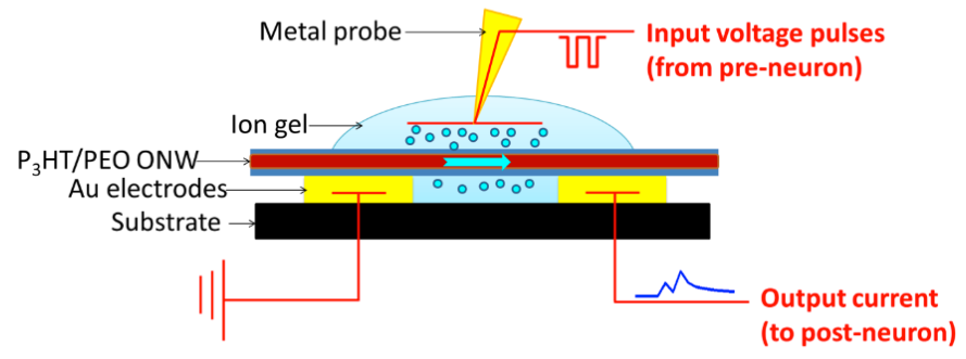
The ONW STs are three-terminal devices. Input voltage pulses that emulate presynaptic spikes from a pre-neuron are applied to the metal probe, which functions as a gate electrode. The input pulses cause ions to migrate in the ion gel, causing a change in the source-drain (yellow rectangles) current flowing through the semiconducting ONW (red). The output current signal — which emulates post-synaptic current flowing to a post-neuron in a biological synapse — is measured (during characterization) by recording the drain current. (credit: Wentao Xu et al./Science Advances)

The artificial synapse devices provide a new research direction in neuromorphic electronics and open a new era of organic electronics with high memory density and low energy consumption, the researchers claim. Potential applications include neuromorphic computing systems, AI systems for self-driving cars, analysis of big data, cognitive systems, robot control, medical diagnosis, stock-trading analysis, remote sensing, and other smart human-interactive systems and machines in the future, they suggest.

This research was supported by the Pioneer Research Center Program and Center for Advanced Soft-Electronics as a Global Frontier Project, funded by the Korean Ministry of Science, ICT, and Future Planning.

The research was published an open-access paper in Science Advances, a new sister journal of Science.

* Prof. Tae-Woo Lee, Wentao Xu, and Sung-Yong Min, PhD, with the Dept. of Materials Science and Engineering at POSTECH

** A fJ (femtojoule) is 10-15 Joule (one watt-second). 

*** ~1014 synapses.

**** Previous attempts to realize synaptic functions in single electronic devices include resistive random access memory (RRAM), phase change memory (PCM), conductive bridges, and synaptic transistors.


Abstract of Organic core-sheath nanowire artificial synapses with femtojoule energy consumption

Emulation of biological synapses is an important step toward construction of large-scale brain-inspired electronics. Despite remarkable progress in emulating synaptic functions, current synaptic devices still consume energy that is orders of magnitude greater than do biological synapses (~10 fJ per synaptic event). Reduction of energy consumption of artificial synapses remains a difficult challenge. We report organic nanowire (ONW) synaptic transistors (STs) that emulate the important working principles of a biological synapse. The ONWs emulate the morphology of nerve fibers. With a core-sheath–structured ONW active channel and a well-confined 300-nm channel length obtained using ONW lithography, ~1.23 fJ per synaptic event for individual ONW was attained, which rivals that of biological synapses. The ONW STs provide a significant step toward realizing low-energy–consuming artificial intelligent electronics and open new approaches to assembling soft neuromorphic systems with nanometer feature size.