Transistor-based biosensor detects molecules linked to cancer, Alzheimer’s, and Parkinson’s

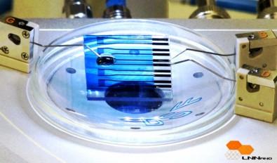
An inexpensive portable biosensor developed by researchers at Brazil’s National Nanotechnology Laboratory (credit: LNNano)

A novel nanoscale organic transistor-based biosensor that can detect molecules associated with neurodegenerative diseases and some types of cancer has been developed by researchers at the National Nanotechnology Laboratory (LNNano) in Brazil.

The transistor, mounted on a glass slide, contains the reduced form of the peptide glutathione (GSH), which reacts in a specific way when it comes into contact with the enzyme glutathione S-transferase (GST), linked to Parkinson’s, Alzheimer’s and breast cancer, among other diseases.

Sensitive water-gated copper phthalocyanine (CuPc) thin-film transistor (credit: Rafael Furlan de Oliveira et al./Organic Electronics)

“The device can detect such molecules even when they’re present at very low levels in the examined material, thanks to its nanometric sensitivity,” explained Carlos Cesar Bof Bufon, Head of LNNano’s Functional Devices & Systems Lab (DSF).

Bufon said the system can be adapted to detect other substances by replacing the analytes (detection compounds). The team is working on paper-based biosensors to further lower the cost, improve portability, and facilitate fabrication and disposal.

The research is published in the journal Organic Electronics.


Abstract of Water-gated phthalocyanine transistors: Operation and transduction of the peptide–enzyme interaction

The use of aqueous solutions as the gate medium is an attractive strategy to obtain high charge carrier density (1012 cm−2) and low operational voltages (<1 V) in organic transistors. Additionally, it provides a simple and favorable architecture to couple both ionic and electronic domains in a single device, which is crucial for the development of novel technologies in bioelectronics. Here, we demonstrate the operation of transistors containing copper phthalocyanine (CuPc) thin-films gated with water and discuss the charge dynamics at the CuPc/water interface. Without the need for complex multilayer patterning, or the use of surface treatments, water-gated CuPc transistors exhibited low threshold (100 ± 20 mV) and working voltages (<1 V) compared to conventional CuPc transistors, along with similar charge carrier mobilities (1.2 ± 0.2) x 10−3 cm2 V−1 s−1. Several device characteristics such as moderate switching speeds and hysteresis, associated with high capacitances at low frequencies upon bias application (3.4–12 μF cm−2), indicate the occurrence of interfacial ion doping. Finally, water-gated CuPc OTFTs were employed in the transduction of the biospecific interaction between tripeptide reduced glutathione (GSH) and glutathione S-transferase (GST) enzyme, taking advantage of the device sensitivity and multiparametricity.

British researchers, Google design modular shape-shifting mobile devices

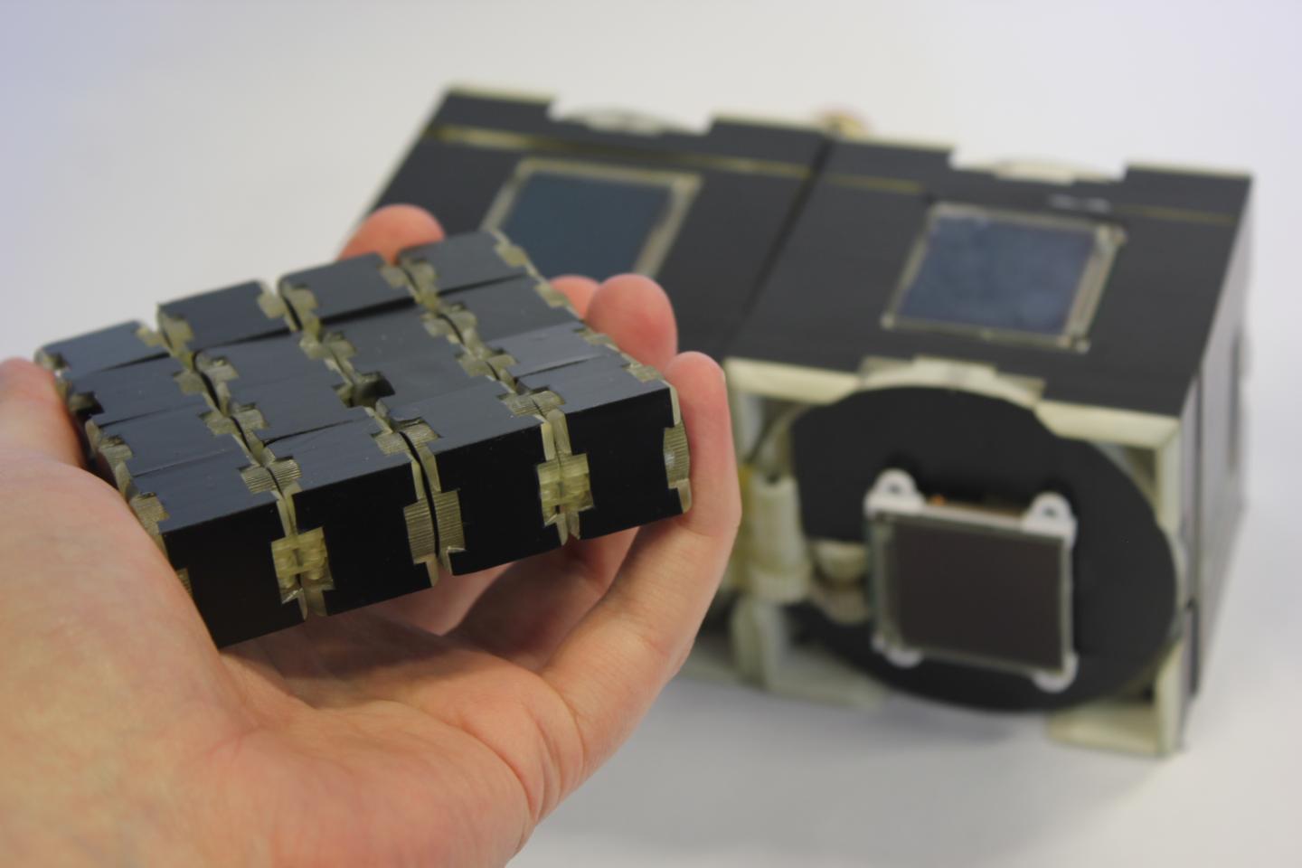
Cubimorph is an interactive device made of a chain of reconfigurable modules that shape-shifts into any shape that can be made out of a chain of cubes, such as transforming from a mobile phone to a game console. (credit: Anne Roudaut et al./Proceedings of the ICRA 2016)

British researchers and Google have independently developed revolutionary concepts for Lego-like modular interactive mobile devices.

The British team’s design, called Cubimorph, is constructed of a chain of cubes. It has touchscreens on each of the six module faces and uses a hinge-mounted turntable mechanism to self-reconfigure in the user’s hand. One example: a mobile phone that can transform into a console when a user launches a game.

Proof-of-concept prototype of Cubimorph (credit: BIG/University of Bristol)

The research team has developed three prototypes demonstrating key aspects — turntable hinges, embedded touchscreens, and miniaturization.


BIG | Cubimorph: Designing Modular Interactive Devices

The modular interactive design is a step toward the vision of programmable matter, where interactive devices change their shape to meet specific user needs.

The research is led by Anne Roudaut, PhD, from the Department of Computer Science at the University of Bristol and and co-leader of the BIG (Bristol Interaction Group), in collaboration with academics at the Universities of PurdueLancaster and Sussex.

The research was presented last week at the International Conference on Robotics and Automation (ICRA).

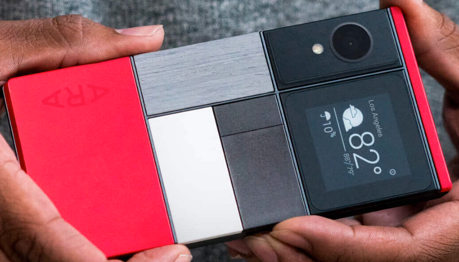
Google’s Ara

Ara (credit: Google)

Ara, launched at Google’s I/O developer conference, uses a frame that contains all the functionality of a smartphone (CPU, GPU, antennas, sensors, battery, and display) plus six flexible slots for easy swapping of modules. “Slide any Ara module into any slot and it just works,” is the concept. Powering this is Greybus, a new bit of software deep in the Android stack that supports instantaneous connections, power efficiency, and data-transfer rates of up to 11.9 Gbps. The Developer Edition will ship in Fall 2016, with a consumer version in 2017.


Google | Ara: What’s next


Abstract of Cubimorph: Designing Modular Interactive Devices

We introduce Cubimorph, a modular interactive device that accommodates touchscreens on each of the six module faces, and that uses a hinge-mounted turntable mechanism to self-reconfigure in the user’s hand. Cubimorph contributes toward the vision of programmable matter where interactive devices reconfigure in any shape that can be made out of a chain of cubes in order to fit a myriad of functionalities, e.g. a mobile phone shifting into a console when a user launches a game. We present a design rationale that exposes user requirements to consider when designing homogeneous modular interactive devices. We present our Cubimorph mechanical design, three prototypes demonstrating key aspects (turntable hinges, embedded touchscreens and miniaturization), and an adaptation of the probabilistic roadmap algorithm for the reconfiguration.

Self-healing, flexible electronic material restores functions after multiple breaks

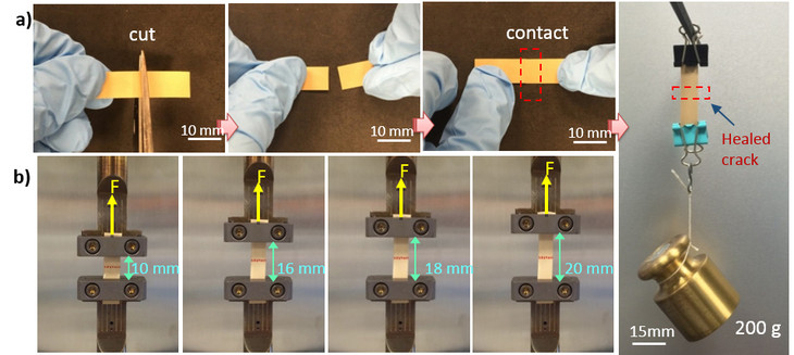
Penn State researchers have developed a flexible electronic material that self-heals to restore multiple functions, even after repeated breaks. (Top row) The material is cut in half, then reattached. After healing for 30 minutes, the material is still able to be stretched and hold weight. (credit: Qing Wang, Penn State)

A new electronic material created by an international team headed by Penn State scientists can heal all its functions automatically, even after breaking multiple times. The new material could improve the durability of wearable electronics.

Electronic materials have been a major stumbling block for the advance of flexible electronics because existing materials do not function well after breaking and healing.

“Wearable and bendable electronics are subject to mechanical deformation over time, which could destroy or break them,” said Qing Wang, professor of materials science and engineering, Penn State. “We wanted to find an electronic material that would repair itself to restore all of its functionality, and do so after multiple breaks.”

In the past, researchers have been able to create self-healable materials (such as these, covered on KurzweilAI) that can restore a single function after breaking. But restoring a suite of functions is critical for creating effective wearable electronics. For example, if a dielectric material retains its electrical resistivity after self-healing but not its thermal conductivity, that could put electronics at risk of overheating.

The material that Wang and his team created restores all properties needed for use as a dielectric in wearable electronics — mechanical strength, breakdown strength to protect against surges, electrical resistivity, thermal conductivity, and dielectric (insulating) properties. They published their findings online in Advanced Functional Materials.

“Most research into self-healable electronic materials has focused on electrical conductivity but dielectrics have been overlooked,” said Wang. “We need conducting elements in circuits but we also need insulation and protection for microelectronics.” Most self-healable materials are also soft or “gum-like,” said Wang, but the material he and his colleagues created is very tough in comparison.

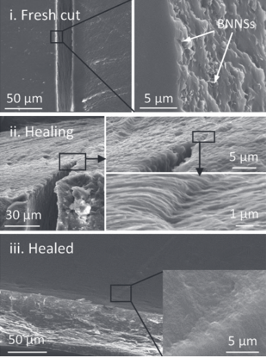
SEM images of healing process of polymer nanocomposite with 8% volume boron nitride nanosheets: (i) freshly cut, (ii) healing in 15 min, and (iii) completely healed in 30 min (credit: Lixin Xing et al./Advanced Functional Materials)

His team added boron nitride nanosheets to a base material of plastic polymer. The material is able to self-heal because boron nitride nanosheets connect to one another with hydrogen bonding groups functionalized onto their surface. When two pieces are placed in close proximity, the electrostatic attraction naturally occurring between both bonding elements draws them close together. When the hydrogen bond is restored, the two pieces are “healed.”

Depending on the percentage of boron nitride nanosheets added to the polymer, this self-healing may require additional heat or pressure, but some forms of the new material can self-heal at room temperature when placed next to each other.

Unlike other healable materials that use hydrogen bonds, boron nitride nanosheets are impermeable to moisture. This means that devices using this dielectric material can operate effectively within high humidity contexts such as in a shower or at a beach.

“This is the first time that a self-healable material has been created that can restore multiple properties over multiple breaks, and we see this being useful across many applications,” said Wang.

Harbin Institute of Technology researches also collaborated on this research, which was supported by the China Scholarship Council.


Penn State Research Communications | Flexible Insulator


Abstract of Self-Healable Polymer Nanocomposites Capable of Simultaneously Recovering Multiple Functionalities

The continuous evolution toward electronics with high power densities and integrated circuits with smaller feature sizes and faster speeds places high demands on a set of material properties, namely, the electrical, thermal, and mechanical properties of polymer dielectrics. Herein, a supramolecular approach is described to self-healable polymer nanocomposites that are mechanically robust and capable of restoring simultaneously structural, electrical, dielectric, and thermal transport properties after multiple fractures. With the incorporation of surface-functionalized boron nitride nanosheets, the polymer nanocomposites exhibit many desirable features as dielectric materials such as higher breakdown strength, larger electrical resistivity, improved thermal conductivity, greater mechanical strength, and much stabilized dielectric properties when compared to the pristine polymer. It is found that the recovery condition has remained the same during sequential cycles of cutting and healing, therefore suggesting no aging of the polymer nanocomposites with mechanical breakdown. Moreover, moisture has a minimal effect on the healing and dielectric properties of the polymer nanocomposites, which is in stark contrast to what is typically observed in the hydrogen-bonded supramolecular structures.

A simple home urine test could scan for diseases


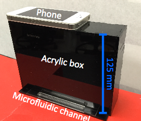
Stanford University School of Engineering | This easy-to-assemble black box is part of an experimental urinalysis testing system designed by Stanford engineers. The black box is meant to enable a smartphone camera to capture video that accurately analyzes color changes in a standard paper dipstick to detect conditions of medical interest.

Two Stanford University electrical engineers have designed a simple new low-cost, portable urinalysis device that could allow patients to get consistently accurate urine test results at home.

The system uses a black box and smartphone camera to analyze a standard color-changing paper test, using a medical dipstick dipped into the urine specimen, to measure levels of glucose, blood, protein, and other chemicals — which can indicate evidence of kidney disease, diabetes, urinary tract infections and even signs of bladder cancer.

The current standard dipstick test uses a paper strip with 10 square pads. Dipped in a sample, each pad changes color to screen for the presence of a different disease-indicating chemical. After waiting the appropriate amount of time, a medical professional — or, increasingly, an automated system — compares the pad shades to a color reference chart for results.

But the test takes time, costs money, and creates backlogs for clinics and primary care physicians. The results are often inconclusive, requiring both patient and doctor to book another appointment. So patients with long-term conditions like chronic urinary tract infections must wait for results to confirm what both patient and doctor already know before getting antibiotics. Tracking patients’ progress with multiple urine tests a day is out of the question.

Some innovators have tried to create simple, do-it-yourself systems, but they can be error-prone, said Audrey (Ellerbee) Bowden, assistant professor of electrical engineering at Stanford. “You think it’s easy — you just dip the stick in urine and look for the color change, but there are things that can go wrong,” she said. “Doctors don’t end up trusting those results as accurate.”

 A simplified home urinanalysis system

Prototype urinalysis device (credit: Gennifer T. Smith et al./Lab on a Chip)

Writing in Lab on a Chip, a journal of the Royal Society of Chemistry, Bowden and Gennifer Smith, a PhD student in electrical engineering, explain they designed their system to overcome three main potential errors in a home test: inconsistent lighting, urine volume control, and timing.

To fix this, the engineers designed a multi-layered system to load urine onto the dipstick. A dropper squeezes urine into a hole in the first layer, filling up a channel in the second layer, and ten square holes in the third layer. Some clever engineering ensures that a uniform volume of urine is deposited on each of the ten pads on the dipstick at just the right time.

Finally, a smartphone is placed on top of the black box with the video camera focused on the dipstick inside the box. Custom software reads video from the smartphone and controls the timing and color analysis.

To perform the test a person would load the urine and then push the third layer into the box. When the third layer hits the back of the box, it signals the phone to begin the video recording at the precise moment when the urine is deposited on the pads.

Timing is critical to the analysis. Pads have readout times ranging from 30 seconds to 2 minutes. Once the two minutes are up, the person can transfer the recording to a software program on their computer. For each pad, it pulls out the frames from the correct time and reads out the results.

The engineers also plan to design an app to send the results directly to the doctor.

Funding for this research came from the National Institutes of Health, the Rose Hills Foundation Graduate Engineering Fellowship, the Electrical Engineering Department New Projects Graduate Fellowship, the Oswald G. Villard Jr. Engineering Fellowship, the Stanford Graduate Fellowship and the National Science Foundation Graduate Research Fellowship.


Abstract of Robust dipstick urinalysis using a low-cost, micro-volume slipping manifold and mobile phone platform

We introduce a novel manifold and companion software for dipstick urinalysis that eliminate many of the aspects that are traditionally plagued by user error: precise sample delivery, accurate readout timing, and controlled lighting conditions. The proposed all-acrylic slipping manifold is reusable, reliable, and low in cost. A simple timing mechanism ensures results are read out at the appropriate time. Results are obtained by capturing videos using a mobile phone and by analyzing them using custom-designed software. We show that the results obtained with the proposed device are as accurate and consistent as a properly executed dip-and-wipe method, the industry gold-standard, suggesting the potential for this strategy to enable confident urinalysis testing in home environments.

Moogfest 2016: the synthesis of future music, technology, and art

Moogfest 2016, a four-day, mind-expanding festival on the synthesis of technology, art, and music, will happen this coming week (Thursday, May 19 to Sunday, May 22) near Duke University in Durham, North Carolina, with more than 300 musical performances, workshops, conversations, masterclasses, film screenings, live scores, sound installations, multiple interactive art experiences, and “The Future of Creativity” keynotes by visionary futurist Martine Rothblatt, PhD. and virtual reality pioneer and author Jaron Lanier.

Cyborg activist Neil Harbisson is the first person in the world with an antenna implanted in his skull, allowing him to hear the frequencies of colors (including infrared and ultraviolet) via bone conduction and receive phone calls. (credit: N. Harbisson)

By day, Moogfest unfolds in venues throughout downtown Durham in spaces that range from intimate galleries and experimental art installations to grand theaters as a platform for geeky exploration and experimentation in sessions and workshops, featuring more than 250 innovators in music, art, and technology, including avant-garde pioneers such as cyborg Neil Harbisson, technoshaman paleo-ecologist/multimedia performer Michael Garfield on “Technoshamanism: A Very Psychedelic Century,” sonifying plants with Data Garden, the Google Magenta (Deep Dream Generator) on training neural networks to generate music, Onyx Ashanti showing how to program music with your mind, Google Doodle’s Ryan Germick, and cyborg artist Moon Ribas, whose cybernetic implants in her arms perceive the movement of real-time earthquakes.

Modular Marketplace 2014 (credit: PatrickPKPR)

Among the fun experimental venues will be the musical Rube Goldberg  workshop, the Global Synthesizer Project (an interactive electronic musical instrument installation where users can synthesize environmental sounds from around the world), THETA (a guided meditation virtual reality spa), WiFi Whisperer (an art installation that visually displays signals around us), the Musical Playground, and Modular Marketplace, an interactive exhibition showcasing the latest and greatest from a lineup of Moog Music and other innovative instrument makers and where the public can engage with new musical devices and their designers; free and open to the public, at the American Tobacco Campus at 318 Blackwell Street from 10am–6pm from May 19–22.


INSTRUMENT 1 from Artiphon will make its public debut at Moogfest 2016. It allows users of any skill or style to strum a guitar, tap a piano, bow a violin, or loop a drum beat — all on a single interface. By connecting to iOS devices, Macs and PCs, this portable musical tool can make any sound imaginable.

In addition, noted MIT Media Lab opera composer/inventor Tod Machover will demonstrate his Hyperinstruments, responsive stage technologies that go beyond multimedia, large-scale collaborative systems and enable entire cities to create symphonies together, and musical tools that promote wellbeing, diagnose disease, and allow for customizing compositions.

Music of the future

By night, Moogfest will present cutting-edge music in venues throughout the city. Performing artists include pioneers in electronic music like Laurie Anderson and legendary synth pioneer Suzanne Ciani, alongside pop and avant-garde experimentalists of today, including Grimes, Explosions in the Sky, Oneohtrix Point Never, Alessandro Cortini, Daniel Lanois, Tim Hecker, Arthur Russell Instrumentals, Rival Consoles, and Dawn of Midi.

Durham’s historic Armory is transformed into a dark and body-thumping dance club to host the best of electronica, house, disco and techno. Godfathers of the genre include The Orb, DJ Harvey, and Robert Hood alongside inspiring new acts such as Bicep (debuting their live show), The Black Madonna and a Ryan Hemsworth curated night including Jlin, Qrion and UVBoi.

“The liberation of LGBTQ+ people is wired into the original components of electronic music culture…” — Artists’ statement here

Local favorite Pinhook features a wide range of experimental sounds: heavy techno from Kyle Hall, Paula Temple and Karen Gwyer, live experimentation from Via App, Patricia, M. Geddes Gengras and Julia Holter, jaggedly rhythmic futurists Rabit and Lotic, and the avante-garde doom metal of The Body.

Moogfest’s largest venue, Motorco Park, is a mix of future-forward electro-pop and R&B with performances by ODESZA, Blood Orange, critically- acclaimed emerging artist DAWN (Dawn Richard) playing her first NC show, he kickoff of Miike Snow’s U.S. Tour, Gary Numan, Silver Apples, Mykki Blanco and newly announced The Range as well as a distinguished hip hop lineup that includes GZA, Skepta, Torey Lanez, Daye Jack, Denzel Curry, Lunice and local artists King Mez, Professor Toon and Well$.

Full Schedule: https://moogfest.sched.org

Robert Moog (credit: Moogarchives.com)

Since 2004, Moogfest has brought together artists, futurist thinkers, inventors, entrepreneurs, designers, engineers, scientists, and musicians. Moogfest is a tribute to Dr. Robert “Bob” Moog and the profound influence his inventions have had on how we hear the world. Over the last sixty years, Bob Moog and Moog Music have pioneered the analog synthesizer and other technology tools for artists. He was vice president for new product research at Kurzweil Music Systems from 1984 to 1988.

This five-fingered robot hand is close to human in functionality

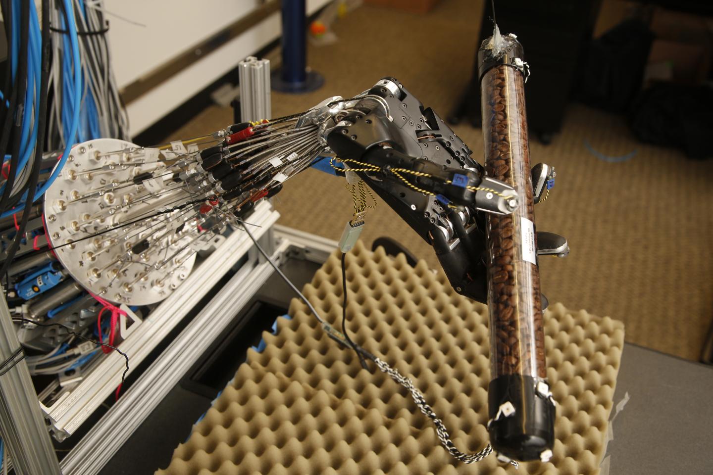
This five-fingered robot hand developed by University of Washington computer science and engineering researchers can learn how to perform dexterous manipulation — like spinning a tube full of coffee beans — on its own, rather than having humans program its actions. (credit: University of Washington)

A University of Washington team of computer scientists and engineers has built what they say is one of the most highly capable five-fingered robot hands in the world. It can perform dexterous manipulation and learn from its own experience without needing humans to direct it.

Their work is described in a paper to be presented May 17 at the IEEE International Conference on Robotics and Automation.

“Hand manipulation is one of the hardest problems that roboticists have to solve,” said lead author Vikash Kumar, a UW doctoral student in computer science and engineering. “A lot of robots today have pretty capable arms but the hand is as simple as a suction cup or maybe a claw or a gripper.”

The UW research team has developed an accurate simulation model that enables a computer to analyze movements in real time. In their latest demonstration, they apply the model to the robot hardware and to real-world tasks like rotating an elongated object.

Autonomous machine learning

With each attempt, the robot hand gets progressively more adept at spinning the tube, thanks to machine learning algorithms that help it model both the basic physics involved and plan which actions it should take to achieve the desired result. (This demonstration begins at 1:47 in the video below.)


University of Washington | ADROIT Manipulation Platform

This autonomous-learning approach developed by the UW Movement Control Laboratory contrasts with robotics demonstrations that require people to program each individual movement of the robot’s hand to complete a single task.

Building a dexterous, five-fingered robot hand poses challenges, both in design and control. The first involved building a mechanical hand with enough speed, strength, responsiveness, and flexibility to mimic basic behaviors of a human hand.

The UW’s dexterous robot hand — which the team built at a cost of roughly $300,000 — uses a Shadow Hand skeleton actuated with a custom pneumatic system and can move faster than a human hand and with 24 degrees of freedom (types of movement). It is too expensive for routine commercial or industrial use, but it allows the researchers to push core technologies and test innovative control strategies.

The team first developed algorithms that allowed a computer to model highly complex five-fingered behaviors and plan movements to achieve different outcomes — like typing on a keyboard or dropping and catching a stick — in simulation. Then they transferred the models to work on the actual five-fingered hand hardware. As the robot hand performs different tasks, the system collects data from various sensors and motion capture cameras and employs machine learning algorithms to continually refine and develop more realistic models.

So far, the team has demonstrated local learning with the hardware system, which means the hand can continue to improve at a discrete task that involves manipulating the same object in roughly the same way. Next steps include beginning to demonstrate global learning, which means the hand could figure out how to manipulate an unfamiliar object or a new scenario it hasn’t encountered before.

The research was funded by the National Science Foundation and the National Institutes of Health.


Abstract of Optimal Control with Learned Local Models: Application to Dexterous Manipulation

We describe a method for learning dexterous manipulation skills with a pneumatically-actuated tendon-driven 24-DoF hand. The method combines iteratively refitted timevarying linear models with trajectory optimization, and can be seen as an instance of model-based reinforcement learning or as adaptive optimal control. Its appeal lies in the ability to handle challenging problems with surprisingly little data. We show that we can achieve sample-efficient learning of tasks that involve intermittent contact dynamics and under-actuation. Furthermore, we can control the hand directly at the level of the pneumatic valves, without the use of a prior model that describes the relationship between valve commands and joint torques. We compare results from learning in simulation and on the physical system. Even though the learned policies are local, they are able to control the system in the face of substantial variability in initial state.

Electronic devices that melt in your brain

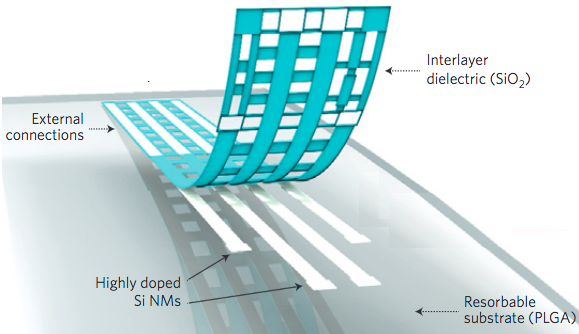
Illustration of the construction of a bioresorbable neural electrode array for ECoG and subdermal EEG measurements. A photolithographically patterned, n-doped silicon nanomaterial (300 nm thick) is used for electrodes and interconnects. A 100 nm thick film of silicon dioxide and a foil of PLGA (30 nm thick) serve as a bioresorbable encapsulating layer and substrate, respectively. The device connects to an external data acquisition system through a conductive film interfaced to the Si nm interconnects at contact pads at the edge. (credit: Ki Jun Yu et al./Nature Materials))

Two implantable devices developed by American and Chinese researchers are designed to dissolve in the brain over time and may eliminate several current problems with implants.

University of Pennsylvania researchers have developed an electrode and an electrode array, both made of layers of silicon and molybdenum that can measure physiological characteristics (like neuron signals) and dissolve at a known rate (determined by the material’s thickness). The team used the device in anesthetized rats to record brain waves (EEGs) and induced epileptic spikes in intact live tissue.

In another experiment, they showed the dissolvable electronics could be used in a complex, multiplexed ECoG (intracranial electroencephalography) array over a 30-day period.

Cartoon illustration of a four-channel bioresorbable electrode array implanted on the left hemisphere of the brain of a rat for chronic recordings. A flexible cable connects the array to a custom-built circular interface board fixed to the skull using dental cement. (credit: Ki Jun Yu et al./Nature Materials)

As the researchers note online in Nature Materials, this new technology offers equal or greater resolution for measuring the brain’s electrical activity, compared to conventional electrodes, while eliminating “the risks, cost, and discomfort associated with surgery to extract current devices used for post-operative monitoring,” according to senior co-author Brian Litt, MD, a professor of Neurology, Neurosurgery, and Bioengineering at the Perelman School of Medicine.

Other potential uses of the dissolvable electronics include:

  • Disorders such as epilepsy, Parkinson’s disease, depression, chronic pain, and conditions of the peripheral nervous system. “These measurements are critically important for mapping and monitoring brain function during and in preparation for neurosurgery, for assisting in device placement, such as for Parkinson’s disease, and for guiding surgical procedures on complex, interconnected nerve structures,” Litt said.
  • Post-operative monitoring and recording of physiological characteristic after minimally invasive placement of vascular, cardiac, orthopaedic, neural or other devices. At present, post-operative monitoring is based on clinical examination or interventional radiology, which is invasive, expensive, and impractical for continuous monitoring over days to months.
  • Heart and brain surgery for applications such as aneurysm coiling, stent placement, embolization, and endoscopic operations. These new devices could also monitor structures that are exposed during surgery, but are too delicate to disturb later by removing devices.
  • More complex devices that also include flow, pressure, and other measurement capabilities.

The research was funded by the Defense Advanced Research Projects Agency, the Penn Medicine Neuroscience Center, a T32- Brain Injury Research Training Grant, the Mirowski Family Foundation, and by Neil and Barbara Smit.

A bioresorbable memristor

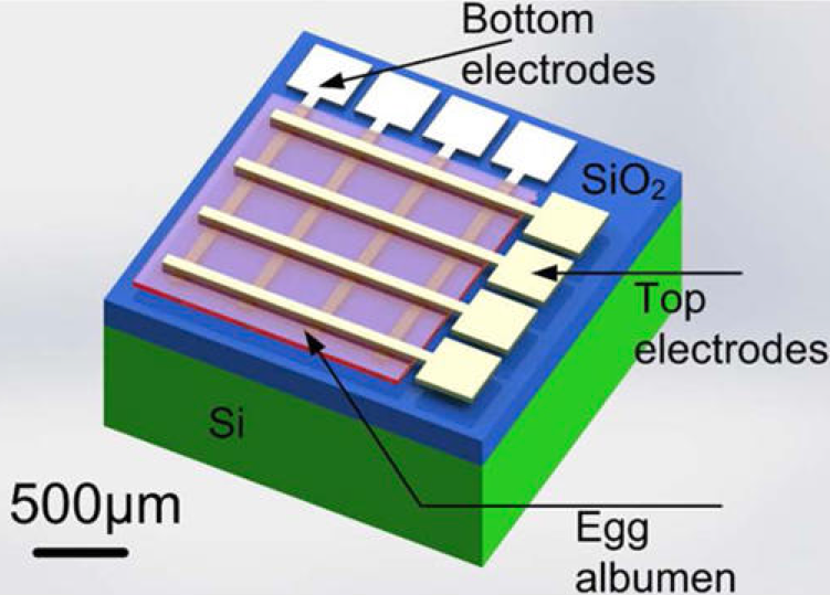
A 3D schematic drawing of cross-bar memristors on a silicon wafer made with dissolvable materials. (credit: Xingli He et al./Applied Materials & Interfaces)

In related research, Chinese researchers have developed a memristor (memory resistor) with biodissolvable components, using a 30 nm film of egg albumin protein on a silicon film substrate and electrodes made out of magnesium and tungsten.*

Testing showed that the device’s bipolar switching performance was comparable to oxide-based memristors, with a high-to-low resistance ratio in the range of 100 to 10,000. The device can store information for more than 10,000 seconds without any deterioration, showing its high stability and reliability.

Under dry conditions in the lab, the components worked reliably for more than three months. In water, the electrodes and albumin dissolved in two to 10 hours in the lab. The rest of the chip took about three days to break down, leaving minimal residues behind, the researchers report in the journal ACS Applied Materials & Interfaces.

The research was funded by the National Natural Science Foundation of China and the Research Fund for the Doctoral Program of Higher Education of China.

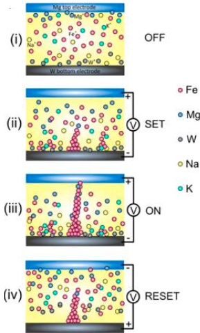
* Memristors may have future applications in nanoelectronic memories, computer logic, and neuromorphic/neuromemristive computer architectures. As shown in the following illustration, redox (oxidation and reduction) of iron molecules in albumen are primarily responsible for this memristor’s switching behavior. However, both Mg and W electrodes can dissolve in water easily and were shown to diffuse into the albumen film, where they also contribute to the formation of conductive filaments through redox reactions.

Schematic of the four switching processes for an albumen-based memristor, showing initial state of a memristor with Mg and W as the top and bottom electrode, respectively. (i) The colored spheres represent different ions. (ii) When a positive voltage is applied to the top electrode, ions move along the electric field, and accumulate locally in strong field regions in the albumen layer; meanwhile, injected electrons from the bottom electrode reduce metallic ions such as Fe3+ and Mg2+ to metal elements. (iii) At a specific voltage, the filaments are formed to connect the top and bottom electrodes electrically, and the device is turned on (the low resistance state). (iv) When applying a reset voltage, the conductive filaments are broken due to the oxidation of the metal elements by the injected electrons from the top electrode, the filaments are ruptured near the top electrode, and the device returns to the high-resistance state. (credit: Xingli He et al./Applied Materials & Interfaces)


Abstract of Bioresorbable silicon electronics for transient spatiotemporal mapping of electrical activity from the cerebral cortex

Bioresorbable silicon electronics technology offers unprecedented opportunities to deploy advanced implantable monitoring systems that eliminate risks, cost and discomfort associated with surgical extraction. Applications include postoperative monitoring and transient physiologic recording after percutaneous or minimally invasive placement of vascular, cardiac, orthopaedic, neural or other devices. We present an embodiment of these materials in both passive and actively addressed arrays of bioresorbable silicon electrodes with multiplexing capabilities, which record in vivo electrophysiological signals from the cortical surface and the subgaleal space. The devices detect normal physiologic and epileptiform activity, both in acute and chronic recordings. Comparative studies show sensor performance comparable to standard clinical systems and reduced tissue reactivity relative to conventional clinical electrocorticography (ECoG) electrodes. This technology offers general applicability in neural interfaces, with additional potential utility in treatment of disorders where transient monitoring and modulation of physiologic function, implant integrity and tissue recovery or regeneration are required.


Abstract of Transient Resistive Switching Devices Made from Egg Albumen Dielectrics and Dissolvable Electrodes

Egg albumen as the dielectric, and dissolvable Mg and W as the top and bottom electrodes are used to fabricate water-soluble memristors. 4 × 4 cross-bar configuration memristor devices show a bipolar resistive switching behavior with a high to low resistance ratio in the range of 1 × 10² to 1 × 10⁴, higher than most other biomaterial-based memristors, and a retention time over 104 s without any sign of deterioration, demonstrating its high stability and reliability. Metal filaments accompanied by hopping conduction are believed to be responsible for the switching behavior of the memory devices. The Mg and W electrodes, and albumen film all can be dissolved in water within 72 h, showing their transient characteristics. This work demonstrates a new way to fabricate biocompatible and dissolvable electronic devices by using cheap, abundant, and 100% natural materials for the forthcoming bioelectronics era as well as for environmental sensors when the Internet of things takes off.

WiFi capacity doubled at less than half the size

Columbia University engineering researchers have developed a new “circulator” technology that can double WiFi speed while reducing the size of wireless devices. It does this by requiring only one antenna (instead of two, for transmitter and receiver) and by using conventional CMOS chips instead of resorting to large, expensive magnetic components.

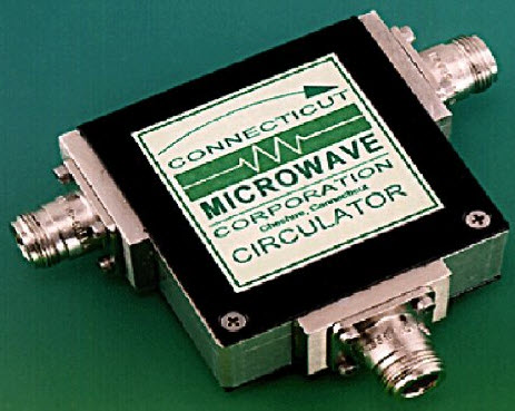
Current bulky circulator design (credit: Connecticut Microwave Corporation)

Columbia engineers previously invented a “full-duplex” radio integrated circuit on a conventional CMOS chip. “Full duplex” means simultaneous transmission and reception at the same frequency in a wireless radio, unlike “half-duplex” (transmitting and receiving at different times, used by current cell phones and other wireless devices). Full duplex also allows for faster transmission speeds.

The new circulator technology further miniaturizes future WiFi and other wireless devices (see Lighter, cheaper radio-wave device could double the useful bandwidth in wireless communications — an earlier circulator device developed by The University of Texas at Austin engineers that was not integrated on a CMOS chip).

“Full-duplex communications, where the transmitter and the receiver operate at the same time and at the same frequency, has become a critical research area and now we’ve shown that WiFi capacity can be doubled on a nanoscale silicon chip with a single antenna,” said Electrical Engineering Associate Professor Harish Krishnaswamy, director of the Columbia High-Speed and Mm-wave IC (CoSMIC) Lab. “This has enormous implications for devices like smartphones and tablets.”

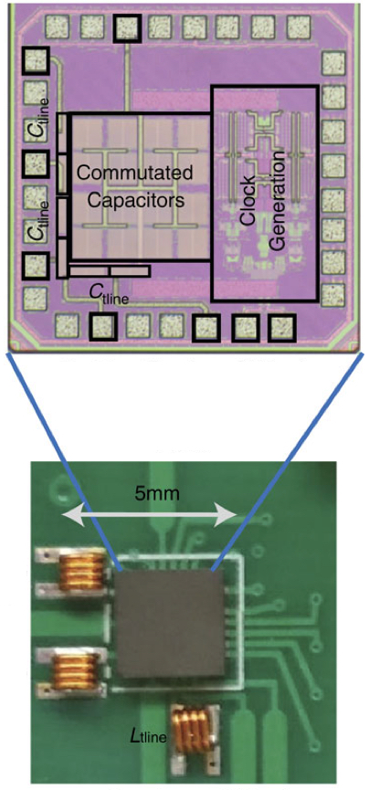
Prototype of first CMOS full-duplex receiver IC with integrated magnetic-free circulator (credit: Negar Reiskarimian, Columbia Engineering)

By combining circulator and full-duplex technologies, “this technology could revolutionize the field of telecommunications,” he said. “Our circulator is the first to be put on a silicon chip, and we get literally orders of magnitude better performance than prior work.”

How to embed circulator technology on a CMOS chip

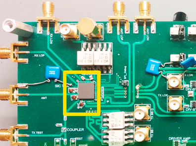
CMOS circulator IC on a printed-curcuit board, interfaced with off-chip inductors. (credit: Negar Reiskarimian, Columbia Engineering)

A circulator allows for using only one antenna to both transmit and receive. To do that, it has to “break” “Lorentz reciprocity” — a fundamental physical characteristic of most electronic structures that requires that electromagnetic waves travel in the same manner in both forward and reverse directions.

The traditional way of breaking Lorentz reciprocity and building radio-frequency circulators has been to use magnetic materials such as ferrites, which lose reciprocity when an external magnetic field is applied. But these materials are not compatible with silicon chip technology, and ferrite circulators are bulky and expensive.

Krishnaswamy and his team were able to design a highly miniaturized circulator that uses switches to rotate the signal across a set of capacitors to emulate the non-reciprocal “twist” of the signal that is seen in ferrite materials.

“Being able to put the circulator on the same chip as the rest of the radio has the potential to significantly reduce the size of the system, enhance its performance, and introduce new functionalities critical to full duplex,” says PhD student Jin Zhou, who integrated the circulator with a full-duplex receiver.

Circulator circuits and components have applications in many different scenarios, from radio-frequency full-duplex communications and radar to building isolators that prevent high-power transmitters from being damaged by back-reflections from the antenna. The ability to break reciprocity also opens up new possibilities in radio-frequency signal processing that are yet to be discovered.

The circulator research is published in an open-access paper on April 15 in Nature Communications. A paper detailing the single-chip full-duplex radio with the circulator and additional echo cancellation was presented at the 2016 IEEE International Solid-State Circuits Conference on February 2.

The work has been funded by the DARPA Microsystems Technology Office and the National Science Foundation.


Abstract of Magnetic-free non-reciprocity based on staggered commutation

Lorentz reciprocity is a fundamental characteristic of the vast majority of electronic and photonic structures. However, non-reciprocal components such as isolators, circulators and gyrators enable new applications ranging from radio frequencies to optical frequencies, including full-duplex wireless communication and on-chip all-optical information processing. Such components today dominantly rely on the phenomenon of Faraday rotation in magneto-optic materials. However, they are typically bulky, expensive and not suitable for insertion in a conventional integrated circuit. Here we demonstrate magnetic-free linear passive non-reciprocity based on the concept of staggered commutation. Commutation is a form of parametric modulation with very high modulation ratio. We observe that staggered commutation enables time-reversal symmetry breaking within very small dimensions (λ/1,250 × λ/1,250 in our device), resulting in a miniature radio-frequency circulator that exhibits reduced implementation complexity, very low loss, strong non-reciprocity, significantly enhanced linearity and real-time reconfigurability, and is integrated in a conventional complementary metal–oxide–semiconductor integrated circuit for the first time.


Abstract of Receiver with integrated magnetic-free N-path-filter-based non-reciprocal circulator and baseband self-interference cancellation for full-duplex wireless

Full-duplex (FD) is an emergent wireless communication paradigm where the transmitter (TX) and the receiver (RX) operate at the same time and at the same frequency. The fundamental challenge with FD is the tremendous amount of TX self-interference (SI) at the RX. Low-power applications relax FD system requirements [1], but an FD system with -6dBm transmit power, 10MHz signal bandwidth and 12dB NF budget still requires 86dB of SI suppression to reach the -92dBm noise floor. Recent research has focused on techniques for integrated self-interference cancellation (SIC) in FD receivers [1-3]. Open challenges include achieving the challenging levels of SIC through multi-domain cancellation, and low-loss shared-antenna (ANT) interfaces with high TX-to-RX isolation. Sharedantenna interfaces enable compact form factor, translate easily to MIMO, and ease system design through channel reciprocity.

Skull echoes could become the new passwords for augmented-reality glasses

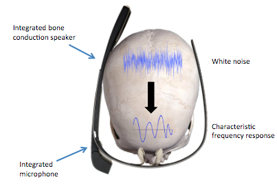
SkullConduct uses the bone conduction speaker and microphone integrated into some augmented-reality glasses and analyzes the characteristic frequency response of an audio signal sent through the user’s skull as a biometric system. (credit: Stefan Schneegass et al./Proc. ACM SIGCHI Conference on Human Factors in Computing Systems)

German researchers have developed a biometric system called SkullConduct that uses bone conduction of sound through the user’s skull for secure user identification and authentication on augmented-reality glasses, such as Google Glass, Meta 2, and HoloLens.

SkullConduct uses the microphone already built into many of these devices and adds electronics (such as a chip) to analyze the frequency response of sound after it travels through the user’s skull. The researchers, at the University of Stuttgart, Saarland University, and Max Planck Institute for Informatics, found that individual differences in skull anatomy result in highly person-specific frequency responses that can be used as a biometric system.

The recognition pipeline used to authenticate users: (1) white noise is played back using the bone conduction speaker, (2) the user’s skull influences the signal in a characteristic way, (3) MFCC features are extracted, and (4) a neuron-network algorithm is used for classification. (credit: Stefan Schneegass et al./Proc. ACM SIGCHI Conference on Human Factors in Computing Systems)

The system combines “Mel Frequency Cepstral Coefficient” (MFCC) (a feature extraction method used in automatic speech recognition) with a lightweight neural-network classifier algorithm that can directly run on the augmented-reality device.

The researchers also conducted a controlled experiment with ten participants that showed that skull-based frequency response serves as a robust biometric, even when taking off and putting on the device multiple times. The experiments showed that the system could identify users with 97.0% accuracy and authenticate them with an error rate of 6.9%.

It’s not as accurate as the CEREBRE biometric system (see You can now be identified by your ‘brainprint’ with 100% accuracy), but it’s low-cost, portable, and doesn’t require a complex system and extensive user testing.


Abstract of SkullConduct: Biometric User Identification on Eyewear Computers Using Bone Conduction Through the Skull

Secure user identification is important for the increasing number of eyewear computers but limited input capabilities pose significant usability challenges for established knowledge-based schemes, such as a passwords or PINs. We present SkullConduct, a biometric system that uses bone conduction of sound through the user’s skull as well as a microphone readily integrated into many of these devices, such as Google Glass. At the core of SkullConduct is a method to analyze the characteristic frequency response created by the user’s skull using a combination of Mel Frequency Cepstral Coefficient (MFCC) features as well as a computationally light-weight 1NN classifier. We report on a controlled experiment with 10 participants that shows that this frequency response is person-specific and stable – even when taking off and putting on the device multiple times – and thus serves as a robust biometric. We show that our method can identify users with 97.0% accuracy and authenticate them with an equal error rate of 6.9%, thereby bringing biometric user identification to eyewear computers equipped with bone conduction technology.

Ultrasound allows for transmitting HD video through animal tissues

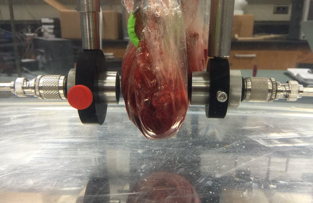
HD video transmission through human tissue from implanted medical devices via in-body ultrasonic communications: beef liver and pork loin were used to represent the density and moisture content found in human tissue (credit: UIUC)(credit: UIUC)

University of Illinois at Urbana-Champaign engineers have demonstrated real-time video-rate (>30Mbps) “meat comm” data transmission through tissue, which could mean in-body ultrasonic communications may be possible for implanted medical devices, including hi-def video.

For example, a patient could swallow a miniaturized HD video camera that could stream live to an external screen, with the orientation of the device controlled wirelessly and externally by a physician, according to Andrew Singer, the Fox Family Professor in the Department of Electrical and Computer Engineering at Illinois,

“To our knowledge, this is the first time anyone has ever sent such high data rates through animal tissue,” Singer added. “These data rates are sufficient to allow real-time streaming of high definition video, enough to watch Netflix, for example, and to operate and control small devices within the body.”

Ingestible cameras and other devices

Potential biomedical uses include ingestible cameras for imaging the digestive track, as well as lower-bandwidth devices such as implanted pacemakers and defibrillators, glucose monitors and insulin pumps, intracranial pressure sensors, and epilepsy control.

Currently, most implanted medical devices use RF electromagnetic waves to communicate through the body. The Federal Communications Commission (FCC) regulates the bandwidths that can be used for RF electromagnetic wave propagation available to implanted medical devices. For example, the Medical Device Radiocommunication Service (MDRS) designates frequencies of operation ranging from 401–406 MHz (where these is high absorption). The corresponding maximum bandwidth allowed is 300 kHz and a maximum of 50 kb/s.

The main limitation for using RF electromagnetic waves in the body is loss of signal that occurs because of attenuation in the body. That requires higher power, which can cause tissue damage from heating due to absorption.

“For underwater applications, radio-frequency (RF) electromagnetic communications has long since been supplanted by acoustic communication,” Singer noted. “Acoustic or ultrasonic communication is the preferred communication means underwater because sound (pressure) waves exhibit dramatically lower losses than RF and can propagate tremendous distances for signals of modest bandwidth.”

The study was reported in an open-access paper on arXiv.org. The researchers have received a provisional patent application on the high-definition ultrasonic technology. They will be presenting their findings at the 17th IEEE International Workshop on Signal Processing  Advances in Wireless Communications, this July in Edinburgh, UK.


Abstract of Mbps Experimental Acoustic Through-Tissue Communications: MEAT-COMMS

Methods for digital, phase-coherent acoustic communication date to at least the work of Stojanjovic, et al [20], and the added robustness afforded by improved phase tracking and compensation of Johnson, et al [21]. This work explores the use of such methods for communications through tissue for potential biomedical applications, using the tremendous bandwidth available in commercial medical ultrasound transducers. While long-range ocean acoustic experiments have been at rates of under 100kbps, typically on the order of 1- 10kbps, data rates in excess of 120Mb/s have been achieved over cm-scale distances in ultrasonic testbeds [19]. This paper describes experimental transmission of digital communication signals through samples of real pork tissue and beef liver, achieving data rates of 20-30Mbps, demonstrating the possibility of real-time video-rate data transmission through tissue for inbody ultrasonic communications with implanted medical devices.