Artificial protein controls first self-assembly of C60 fullerenes

Buckminsterfullerene (C60), aka fullerene and buckyball (credit: St Stev via Foter.com / CC BY-NC-ND)

A Dartmouth College scientist and his collaborators* have created the first high-resolution co-assembly between a protein and buckminsterfullerene (C60), aka fullerene and buckyball (a sphere-like molecule composed of 60 carbon atoms and shaped like a soccer ball).

“This is a proof-of-principle study demonstrating that proteins can be used as effective vehicles for organizing nanomaterials by design,” says senior author Gevorg Grigoryan, an assistant professor of computer science at Dartmouth and senior author of a study discussed in an open-access paper in the journal in Nature Communications.

Proteins organize and orchestrate essentially all molecular processes in our cells. The goal of the new study was to create a new artificial protein that can direct the self-assembly of fullerene into ordered superstructures.

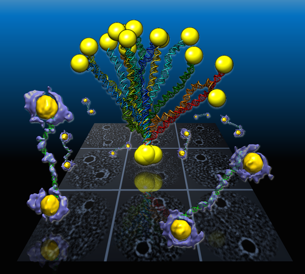
COP, a stable tetramer (a polymer derived from four identical single molecule) in isolation, interacts with C60 (fullerene) molecules via a surface-binding site and further self-assembles into a co-crystalline array called C60Sol–COP (credit: Kook-Han Kim et al./Nature Communications)

Grigoryan and his colleagues show that that their artificial protein organizes a fullerene into a lattice called C60Sol–COP. COP, a protein that is a stable tetramer (a polymer derived from four identical single molecules), interacted with fullerene molecules via a surface-binding site and further self-assembled into an ordered crystalline superstructure. Interestingly, the superstructure exhibits high charge conductance, whereas both the protein-alone crystal and amorphous C60 are electrically insulating.

Grigoryan says that if we learn to do the programmable self-assembly of precisely organized molecular building blocks more generally, it will lead to a range of new materials with properties such as higher strength, lighter weight, and greater chemical reactivity, resulting in a host of applications, from medicine to energy and electronics.

Fullerenes are currently used in nanotechnology because of their high heat resistance and electrical superconductivity (when doped), but the molecule has been difficult to organize in useful ways.

* The study also included researchers from Dartmouth College, Sungkyunkwan University, the New Jersey Institute of Technology, the National Institute of Science Education and Research, the University of California-San Francisco, the University of Pennsylvania, and the Institute for Basic Science.


Abstract of Protein-directed self-assembly of a fullerene crystal

Learning to engineer self-assembly would enable the precise organization of molecules by design to create matter with tailored properties. Here we demonstrate that proteins can direct the self-assembly of buckminsterfullerene (C60) into ordered superstructures. A previously engineered tetrameric helical bundle binds C60 in solution, rendering it water soluble. Two tetramers associate with one C60, promoting further organization revealed in a 1.67-Å crystal structure. Fullerene groups occupy periodic lattice sites, sandwiched between two Tyr residues from adjacent tetramers. Strikingly, the assembly exhibits high charge conductance, whereas both the protein-alone crystal and amorphous C60 are electrically insulating. The affinity of C60 for its crystal-binding site is estimated to be in the nanomolar range, with lattices of known protein crystals geometrically compatible with incorporating the motif. Taken together, these findings suggest a new means of organizing fullerene molecules into a rich variety of lattices to generate new properties by design.

How to make the world’s fastest flexible silicon transistor

World’s fastest silicon-based flexible transistors, shown here on a plastic substrate (credit: Jung-Hun Seo/UW–Madison)

A team headed by University of Wisconsin—Madison engineers has fabricated a flexible transistor that operates at a record 38 gigahertz, but may be able to operate at 110 gigahertz.

The process could allow manufacturers to easily and cheaply fabricate high-performance transistors with wireless capabilities, using a radical fabrication method based on huge rolls of flexible plastic.

The new transistor can also transmit data or transfer power wirelessly, which could unlock advances in a whole host of applications ranging from wearable electronics to sensors.

Low-cost radical method uses less energy, achieves higher transistor density

The researchers’ nanoscale fabrication method (based on a simple, low-cost process called nanoimprint lithography) replaces conventional lithographic approaches — which use light and chemicals to pattern flexible transistors — overcoming such limitations as light diffraction, imprecision that leads to short circuits of different contacts, and the need to fabricate the circuitry in multiple passes.

The researchers — led by Zhenqiang (Jack) Ma, the Lynn H. Matthias Professor in Engineering and Vilas Distinguished Achievement Professor in electrical and computer engineering, and research scientist Jung-Hun Seo —  published details of the advance Wednesday April 20 in an open-access paper in the journal Scientific Reports.

With a unique, three-dimensional current-flow pattern, the high-performance transistor consumes less energy and operates more efficiently. And because the researchers’ method enables them to slice much narrower trenches than conventional fabrication processes can, it also could enable semiconductor manufacturers to squeeze an even greater number of transistors onto an electronic device.

Ultimately, says Ma, because the mold can be reused, the method could easily scale for use in a technology called roll-to-roll processing (think of a giant, patterned rolling pin moving across sheets of plastic the size of a tabletop), and that would allow semiconductor manufacturers to repeat their pattern and mass-fabricate many devices on a roll of flexible plastic.

“Nanoimprint lithography addresses future applications for flexible electronics,” says Ma, whose work was supported by the Air Force Office of Scientific Research. “We don’t want to make them the way the semiconductor industry does now. Our step, which is most critical for roll-to-roll printing, is ready.”

The process

  1. Using low-temperature processes, the researchers patterned the transistor circuitry using nanoimprint lithography.
  2. Using selective doping, the researchers introduced impurities into materials in precise locations to enhance their properties — in this case, electrical conductivity. Currently, the dopant sometimes merges into areas of the material it shouldn’t, causing what is known as the “short channel” effect. The researchers took an unconventional approach: They blanketed their single crystalline silicon with a dopant, rather than selectively doping it.
  3. They added a light-sensitive material, or photoresist layer, and used a technique called electron-beam lithography — which uses a focused beam of electrons to create shapes as narrow as 10 nanometers wide — on the photoresist to create a reusable mold of the nanoscale patterns they desired. They applied the mold to an ultrathin, very flexible silicon membrane to create a photoresist pattern.
  4. They finished with a dry-etching process — essentially, a nanoscale knife — that cut precise, nanometer-scale trenches in the silicon following the patterns in the mold, and added wide gates, which function as switches, atop the trenches.

Additional authors are at UW–Madison, the University of Michigan, the University of Texas at Arlington, and the University of California, Berkeley.


Abstract of Fast Flexible Transistors with a Nanotrench Structure

The simplification of fabrication processes that can define very fine patterns for large-area flexible radio-frequency (RF) applications is very desirable because it is generally very challenging to realize submicron scale patterns on flexible substrates. Conventional nanoscale patterning methods, such as e-beam lithography, cannot be easily applied to such applications. On the other hand, recent advances in nanoimprinting lithography (NIL) may enable the fabrication of large-area nanoelectronics, especially flexible RF electronics with finely defined patterns, thereby significantly broadening RF applications. Here we report a generic strategy for fabricating high-performance flexible Si nanomembrane (NM)-based RF thin-film transistors (TFTs), capable of over 100 GHz operation in theory, with NIL patterned deep-submicron-scale channel lengths. A unique 3-dimensional etched-trench-channel configuration was used to allow for TFT fabrication compatible with flexible substrates. Optimal device parameters were obtained through device simulation to understand the underlying device physics and to enhance device controllability. Experimentally, a record-breaking 38 GHz maximum oscillation frequency fmax value has been successfully demonstrated from TFTs with a 2 μm gate length built with flexible Si NM on plastic substrates.

A battery you never have to replace

Top: Schematic diagram of all-nanowire-based capacitor (similar to a battery), using gold-manganese dioxide conductors and PMMA gel layer. Bottom: photograph of the capacitor containing 750 parallel nanowire loops patterned onto a glass microscope slide. (credit: Mya Le Thai/ACS Energy Lett.)

University of California, Irvine researchers have invented a new nanowire-based battery material that can be recharged hundreds of thousands of times, moving us closer to a battery that would never require replacement.

It could lead to commercial batteries with greatly lengthened lifespans for computers, smartphones, appliances, cars, and spacecraft.

The design is based on nanowires, which are highly conductive and feature a large surface area for the storage and transfer of electrons.

Currently, nanowires are extremely fragile and don’t hold up well to repeated discharging and recharging (cycling). In a typical lithium-ion battery, they expand and grow brittle, which leads to cracking.

UCI researchers have solved this problem by coating a gold nanowire in a manganese dioxide shell and encasing the assembly in an electrolyte made of a Plexiglas-like gel. The liquid electrolyte is replaced with a poly(methyl methacrylate) (PMMA) gel electrolyte. The combination is reliable and resistant to failure.

The study leader, UCI doctoral candidate Mya Le Thai, cycled the testing electrode up to 200,000 times over three months without detecting any loss of capacity or power and without fracturing any nanowires. The findings were published Wednesday Apr. 20 in an open-access paper in the American Chemical Society’s Energy Letters.

“Mya was playing around, and she coated this whole thing with a very thin gel layer and started to cycle it,” said senior author Reginald Penner, chair of UCI’s chemistry department. “She discovered that just by using this gel, she could cycle it hundreds of thousands of times without losing any capacity. That was crazy, because these things typically die in dramatic fashion after 5,000 or 6,000 or 7,000 cycles at most.”

The researchers think the gel plasticizes the metal oxide in the battery and gives it flexibility, preventing cracking.

“The coated electrode holds its shape much better, making it a more reliable option,” Thai said. “This research proves that a nanowire-based battery electrode can have a long lifetime and that we can make these kinds of batteries a reality.”


Abstract of 100k Cycles and Beyond: Extraordinary Cycle Stability for MnO2 Nanowires Imparted by a Gel Electrolyte

We demonstrate reversible cycle stability for up to 200 000 cycles with 94–96% average Coulombic efficiency for symmetrical δ-MnO2 nanowire capacitors operating across a 1.2 V voltage window in a poly(methyl methacrylate) (PMMA) gel electrolyte. The nanowires investigated here have a Au@δ-MnO2 core@shell architecture in which a central gold nanowire current collector is surrounded by an electrodeposited layer of δ-MnO2 that has a thickness of between 143 and 300 nm. Identical capacitors operating in the absence of PMMA (propylene carbonate (PC), 1.0 M LiClO4) show dramatically reduced cycle stabilities ranging from 2000 to 8000 cycles. In the liquid PC electrolyte, the δ-MnO2 shell fractures, delaminates, and separates from the gold nanowire current collector. These deleterious processes are not observed in the PMMA electrolyte.

Ultrathin organic material enhances e-skin displays

Top left: System outline of a blood oxygen level monitor. Top right: Red and green polymer light-emitting diodes (PLEDs) are directed to shine into the finger. Reflected light from inside the finger is caught by an ultraflexible organic photodetector. This reflected light provides a measure of blood oxygen and pulse rate. Bottom: The output of the sensor can be shown on a PLED display. (credit: Someya Laboratory)

University of Tokyo researchers have developed technology to enable creation of electronic skin (e-skin) displays of blood oxygen level, e-skin heart rate sensors for medical, athletic uses, and other applications.

To serve as a demo, they’ve created an ultrathin, ultraflexible, protective layer and created an air-stable, organic light-emitting diode (OLED) display.

For use in electronic devices integrated into the human body, wearable electronics need to be thin and flexible to minimize impact where they attach to the body.

But most devices developed so far have required millimeter-scale-thickness glass or plastic substrates with limited flexibility, and micrometer-scale thin flexible organic devices have not been stable enough to survive in air.

The research group of Professor Takao Someya and Dr. Tomoyuki Yokota at the University of Tokyo’s Graduate School of Engineering has now developed a high-quality protective film less than two micrometers thick that enables the production of ultrathin, ultraflexible, high-performance wearable electronic displays and other devices.

The group developed the protective film by alternating layers of inorganic (Silicon Oxynitrite) and organic (Parylene) material. The protective film prevented passage of oxygen and water vapor in the air, extending device lifetimes from the few hours seen in prior research to several days. In addition, the research group was able to attach transparent indium tin oxide (ITO) electrodes to an ultrathin substrate without damaging it, making the e-skin display possible.

Using the new protective layer and ITO electrodes, the research group created polymer light-emitting diodes (PLEDs) and organic photodetectors (OPDs). These were thin enough to be attached to the skin and flexible enough to distort and crumple in response to body movement.

The PLEDs were just three micrometers thick and more than six times more efficient than previously reported ultrathin PLEDs. This reduced heat generation and power consumption, making them particularly suitable for direct attachment to the body for medical applications such as displays for blood oxygen concentration or pulse rate. The research group also combined red and green PLEDs with a photodetector to demonstrate a blood oxygen sensor.

In addition to medical uses, Someya sees this technology as a kind of ultra mood ring. “The advent of mobile phones has changed the way we communicate. While these communication tools are getting smaller and smaller, they are still discrete devices that we have to carry with us,” he says. “What would the world be like if we had displays that could adhere to our bodies and even show our emotions or level of stress or unease? They might enhance the way we interact with those around us or add a whole new dimension to how we communicate.”


Someya Laboratory | The red seven-segment PLED display in operation on the back of a hand.

Abstract of Ultraflexible organic photonic skin

Thin-film electronics intimately laminated onto the skin imperceptibly equip the human body with electronic components for health-monitoring and information technologies. When electronic devices are worn, the mechanical flexibility and/or stretchability of thin-film devices helps to minimize the stress and discomfort associated with wear because of their conformability and softness. For industrial applications, it is important to fabricate wearable devices using processing methods that maximize throughput and minimize cost. We demonstrate ultraflexible and conformable three-color, highly efficient polymer light-emitting diodes (PLEDs) and organic photodetectors (OPDs) to realize optoelectronic skins (oe-skins) that introduce multiple electronic functionalities such as sensing and displays on the surface of human skin. The total thickness of the devices, including the substrate and encapsulation layer, is only 3 μm, which is one order of magnitude thinner than the epidermal layer of human skin. By integrating green and red PLEDs with OPDs, we fabricate an ultraflexible reflective pulse oximeter. The device unobtrusively measures the oxygen concentration of blood when laminated on a finger. On-skin seven-segment digital displays and color indicators can visualize data directly on the body.

Turning hands and packages into displays

The SkinHaptics device sends ultrasound waves through the hand, focused at a precise point on the palm. (credit: Sri Subramanian / University of Sussex)

Imagine using your hand as an interactive touch-screen display. Sounds like science fiction, but Nokia Research Centre and the European Research Council have funded a study, led by the University of Sussex, to develop such a device, which could be used as a display for the next generation of smartwatches and other smart devices.

Called SkinHaptics, the device (still in the lab) sends ultrasonic pulses to your palm from the back of your hand, creating tactile sensations (similar to the iPhone 6s and Apple Watch “3D Touch” feature, which senses the amount of pressure your finger applies to the screen and can trigger various actions).

SkinHaptics ultrasound transmitter (left) and display (right) (credit: University of Sussex)

SkinHaptics is based on haptics, the science of applying touch sensation and control to interaction with computers and technology. It uses “time-reversal” processing, make the waves converge and become more targeted as they travel through the hand (rather than being dispersed), and ending at a precise point on the palm.

Professor Sriram Subramanian, who leads the research team at the University of Sussex, says technologies will need to engage other senses, such as touch, as we enter what designers are calling an “eye-free” age of technology. “If you imagine you are on your bike and want to change the volume control on your smartwatch, the interaction space on the watch is very small. So companies are looking at how to extend this space to the hand of the user.”

The findings were presented at the IEEE Haptics Symposium 2016 in Philadelphia.


Interact Lab | SkinHaptics: Ultrasound Focused in the Hand Creates Tactile Sensations

Package displays

In another innovative display concept, scientists at the University of Sheffield and technology company Novalia have developed technology for affixing an interactive display to packaging to display a promotion or an instructional label, for example.

This technology could be used in greetings cards or on products that allow a customer to receive a simple message or even ask questions.

(a) Schematic of the capacitive touch-pad array, electrical circuit and LED array. (b) Photo of the integrated electronic system on the printed paper substrate. (credit: University of Sheffield)

In a paper published in the IEEE Journal of Display Technology, the team explains that the process involves printing electronic tracks onto paper, using a low-cost conductive graphite ink, to create capacitive touch pads and then affixing low-cost CMOS electronics and a polymer LED display to the paper, using an adhesive that conducts electricity.

The scientists also designed and constructed a touch-pad keyboard on paper that allows a user to selectively turn LEDs in the display on or off. The process could potentially be printed on other surfaces.

The research has been funded by the Engineering and Physical Sciences Research Council (EPSRC).


Abstract of SkinHaptics: Ultrasound Focused in the Hand Creates Tactile Sensations

Recent developments in on-body interfaces have extended the interaction space of physical devices to the skin of our hands. While these interfaces can easily project graphical elements on the bare hand, they cannot give tactile feedback. Here we present a technology that could help to expand the output capability of on-body interfaces to provide tactile feedback without restricting the skin as an interaction surface. SkinHaptics works by focusing ultrasound in the hand using a phased array of ultrasound transmitters and the acoustic time reversal signal processing technique. We present experimental results that show that this device can steer and focus ultrasound on the skin through the hand, which provides the basis for the envisioned technology. We then present results of a study that show that the focused energy can create sensations that are perceived under the skin and in the hand. We demonstrate the potential of SkinHaptics and discuss how our proof-of-concept device can be scaled beyond the prototype.

Abstract of Polymer Light Emitting Diodes Powered via Paper-mounted Electronics

We have interfaced an array of polymer light emitting diodes (OLEDs) fabricated onto a glass substrate to a sheet of paper via a pressure sensitive conducting adhesive. By screen-printing a series of capacitive touch pads and connecting tracks onto paper using a low-cost conductive graphite ink, we are able to drive individual pixels in the OLED array via CMOS-based electronics that are also attached to the paper. Three AA batteries are used to power the CMOS electronics, touch-pads and the OLED array, with pixels in the array operating at a brightness of up to 210 cd/m2. The work highlights a practical interface between plastic- and paper-based electronics.

​Clothes that receive and transmit digital information

Researchers at The Ohio State University are developing embroidered antennas and circuits with 0.1 mm precision — the perfect size to integrate electronic components such as communication devices, sensors, and computer memory devices into clothing.  (credit: Photo by Jo McCulty, courtesy of The Ohio State University)

Ohio State University researchers have taken a key step in the design of  “functional textiles” — clothes that gather, store, or transmit digital information. They’ve developed a breakthrough method of weaving electronic components into fabric with 0.1mm precision — small enough to integrate components such as sensors and computer memory devices into clothing.

Imagine shirts that act as antennas for your smart phone or tablet, workout clothes that monitor your fitness level, sports equipment that monitors athletes’ performance, a bandage that tells your doctor how well the tissue beneath is healing, or a flexible fabric cap that senses or stimulates activity in the brain (eliminating restrictive tethered external wiring on the patient’s body).

“A revolution is happening in the textile industry,” said John Volakis, director of the ElectroScience Laboratory and the Roy & Lois Chope Chair Professor of Electrical Engineering at Ohio State. “We believe that functional textiles are an enabling technology for communications and sensing — and one day, even medical applications like imaging and health monitoring.”

Recently, he and research scientist Asimina Kiourti refined their patented fabrication method to create prototype wearables at a fraction of the cost and in half the time compared to two years ago. They published the new results in the journal IEEE Antennas and Wireless Propagation Letters.

Cell-phone antennas

Asimina Kiourti, a research scientist at The Ohio State University, demonstrates the embroidery technique she and John Volakis invented for integrating electronics into clothing (photo credit: Jo McCulty/The Ohio State University)

In Volakis’ lab, the functional textiles, also called “e-textiles,” are created in part on a typical tabletop sewing machine. Like other modern sewing machines, it embroiders thread into fabric automatically based on a pattern loaded from a computer file. The researchers substitute the thread with fine silver metal wires that, once embroidered, feel the same as traditional thread to the touch.

“We started with a technology that is very well known — machine embroidery — and we asked: how can we functionalize embroidered shapes? How do we make them transmit signals at useful frequencies, like for cell phones or health sensors?” Volakis said. “Now, for the first time, we’ve achieved the accuracy of printed metal circuit boards, so our new goal is to take advantage of the precision to incorporate receivers and other electronic components.”

Broadband antenna constructed from multiple embroidered geometric shapes, each resonating at a different frequency (photo credit: Jo McCulty/The Ohio State University)

The shape of the embroidery determines the frequency of operation of the antenna or circuit, explained Kiourti. The shape of one broadband antenna, for instance, consists of more than half a dozen interlocking geometric shapes, each a little bigger than a fingernail, that form an intricate circle a few inches across. Each piece of the circle transmits energy at a different frequency, so that they cover a broad spectrum of energies when working together — achieving a “broadband” capability of the antenna for cell phone and Internet access.

In another design, tests showed that an embroidered spiral antenna (top photo) measuring approximately six inches across transmitted signals at frequencies of 1 to 5 GHz with near-perfect efficiency,  well-suited to broadband Internet and cellular communication.


Proposed embroidery process to achieve 0.1mm geometrical precision (credit: Asimina Kiourti et al./IEEE Antennas Wireless Propag. Lett.)

On problem they had was that fine wires couldn’t provide as much surface conductivity as thick wires. So they had to find a way to work the fine thread into embroidery densities and shapes that would boost the surface conductivity and, thus, the antenna/sensor performance.

The new threads have a 0.1-mm diameter, made with only seven filaments. Each filament is copper at the center, enameled with pure silver. They purchase the wire by the spool at a cost of 3 cents per foot; Kiourti estimated that embroidering a single broadband antenna like the one mentioned above consumes about 10 feet of thread, for a material cost of around 30 cents per antenna. That’s 24 times less expensive than when Volakis and Kiourti created similar antennas in 2014.

In part, the cost savings comes from using less thread per embroidery. The researchers previously had to stack the thicker thread in two layers, one on top of the other, to make the antenna carry a strong enough electrical signal. But by refining the technique that she and Volakis developed, Kiourti was able to create the new, high-precision antennas in only one embroidered layer of the finer thread. So now the process takes half the time: only about 15 minutes for the broadband antenna mentioned above.

She’s also incorporated some techniques common to microelectronics manufacturing to add parts to embroidered antennas and circuits. One prototype antenna looks like a spiral and can be embroidered into clothing to improve cell phone signal reception. Another prototype, a stretchable antenna with an integrated RFID (radio-frequency identification) chip embedded in rubber, takes the applications for the technology beyond clothing — for tires, in this case.

The work fits well with Ohio State’s role as a founding partner of the Advanced Functional Fabrics of America Institute, a national manufacturing resource center for industry and government. The new institute, which joins some 50 universities and industrial partners, was announced earlier this month by U.S. Secretary of Defense Ashton Carter.

Syscom Advanced Materials in Columbus provided the threads used in Volakis and Kiourti’s initial work. The finer threads used in this study were purchased from Swiss manufacturer Elektrisola. The research is funded by the National Science Foundation, and Ohio State will license the technology for further development.


Abstract of Fabrication of Textile Antennas and Circuits With 0.1 mm Precision

We present a new selection of E-fibers (also referred to as E-threads) and associated embroidery process. The new E-threads and process achieve a geometrical precision down to 0.1 mm. Thus, for the first time, accuracy of typical printed circuit board (PCB) prototypes can be achieved directly on textiles. Compared to our latest embroidery approach, the proposed process achieves: 1) 3 × higher geometrical precision; 2) 24 × lower fabrication cost; 3) 50% less fabrication time; and 4) equally good RF performance. This improvement was achieved by employing a new class of very thin, 7-filament, Elektrisola E-threads ( diameter ≈ 0.12 mm, almost 2 × thinner than before). To validate our approach, we “printed” and tested a textile spiral antenna operating between 1-5 GHz. Measurement results were in good agreement with simulations. We envision this textile spiral to be integrated within a cap and unobtrusively acquire neuropotentials from wireless fully-passive brain implants. Overall, the proposed embroidery approach brings forward new possibilities for a wide range of applications.

‘Breakthrough Starshot’ aims to reach Alpha Centauri 20 years after launch

Alpha Centauri (credit: ESO Online Digitized Sky Survey)

Internet investor and science philanthropist Yuri Milner and physicist Stephen Hawking announced Tuesday a $100 million research and engineering program, Breakthrough Starshot, aiming to demonstrate proof of concept for light-propelled “nanocrafts” that could travel to Alpha Centauri, our nearest star system.

The nanocrafts would fly at 20 percent of light speed and capture images of possible planets and other scientific data, arriving in just over 20 years after their launch.

“Earth is a wonderful place, but it might not last forever,” said Hawking. “Sooner or later, we must look to the stars. Breakthrough Starshot is a very exciting first step on that journey.”

Breakthrough Starshot program

L-R) Yuri Milner, Breakthrough Prize and DST Global Founder; Stephen Hawking, CH, CBE, FRS, Dennis Stanton Avery and Sally Tsui Wong-Avery Director of Research, University of Cambridge; Freeman Dyson, Emeritus Professor, Princeton Institute for Advanced Study; Ann Druyan, Producer, Co-Founder and CEO of Cosmos Studios; Avi Loeb, Frank B. Baird, Jr. Professor of Science at Harvard University; Mae Jamison, Nasa Astronaut, Principal 100 Year Starship Foundation; and Peter Worden, Chairman, Breaktrough Prize Foundation, Former NASA Director speak on stage as Yuri Milner And Stephen Hawking host press conference to announce Breakthrough Starshot, a new space exploration initiative, at One World Observatory on April 12, 2016 in New York City. (Photo by Bryan Bedder/Getty Images for Breakthrough Prize Foundation)

The Breakthrough Starshot program will be led by Pete Worden, the former director of NASA AMES Research Center, and advised by a committee of world-class scientists and engineers. The board will consist of Stephen Hawking, Yuri Milner, and Mark Zuckerberg.

Nanocrafts

Nanocraft, comprising Lightsail and StarChip powered by Light Beamer (credit: Breakthrough Initiatives)

The Alpha Centauri star system is 25 trillion miles (4.37 light years) away. With today’s fastest spacecraft, it would take about 30,000 years to get there. The program aims to establish whether a gram-scale nanocraft on a sail pushed by a light beam can fly more than 1,000 times faster.

Nanocrafts are gram-scale robotic spacecrafts, comprising:

Starchip (credit: Breakthrough Initiatives)

Starchip: a gram-scale wafer carrying cameras, photon thrusters, power supply, navigation, and communication equipment, and constituting a fully functional space probe.

Lightsail (credit: Breakthrough Initiatives)

Lightsail: Advances in nanotechnology are producing increasingly thin and lightweight materials, promising to enable the fabrication of meter-scale sails no more than a few hundred atoms thick and at gram-scale mass.

Light Beamer (credit: Breakthrough Initiatives)

Light Beamer. The rising power and falling cost of lasers has led to significant advances in light-beaming technology. Phased arrays of lasers (the “light beamer”) could potentially be scaled up to the 100 gigawatt level.

Breakthrough Starshot aims to bring economies of scale to the astronomical scale. The StarChip can be mass-produced at the cost of an iPhone and be sent on missions in large numbers to provide redundancy and coverage. The light beamer is modular and scalable. Once it is assembled and the technology matures, the cost of each launch is expected to fall to a few hundred thousand dollars.


Breakthrough Starshot

Path to the stars

The research and engineering phase is expected to last a number of years. Following that, development of the ultimate mission to Alpha Centauri would require a budget comparable to the largest current scientific experiments, and would involve building a ground-based kilometer-scale light beamer at high altitude in dry conditions, powered by a few gigawatt hours of energy per launch.

The plan is to launching a “mothership” carrying thousands of nanocrafts to a high-altitude orbit, taking advantage of adaptive optics technology in real time to compensate for atmospheric effects. Focusing the light beam on the lightsail would accelerate individual nanocrafts to the target speed within minutes.

The goal is to capture images of a planet and other scientific data and transmitting them back to Earth using a compact on-board laser communications system, using the same light beamer that launched the nanocrafts to receive data from them over 4 years later.

The organizers acknowledge that these and other system requirements represent significant engineering challenges, but are based on technology either already available or likely to be attainable in the near future under reasonable assumptions, the organizers say.

Kilometer-scale telescope

The proposed light propulsion system is at a scale that calls for global cooperation and support. Clearance for launches would be required from all the appropriate government and international organizations.

As the technology required for interstellar travel matures, a number of additional opportunities will emerge, including contributions to solar system exploration, using the light beamer as a kilometer-scale telescope for astronomical observations, and detection of Earth-crossing asteroids at large distances.

Astronomers estimate that there is a reasonable chance of an Earth-like planet existing in the “habitable zones” of Alpha Centauri’s three-star system. A number of scientific instruments, ground-based and space-based, are being developed and enhanced, which will soon identify and characterize planets around nearby stars. A separate Breakthrough Initiative will support some of these projects.

Getting it off the ground

The Breakthrough Starshot initiative is based entirely on research in the public domain. It will be dedicated to full transparency and open access, and open to experts in all relevant fields as well as the public to contribute ideas through its online forum.  The initiative will establish a research grant program, and will make available other funding to support relevant scientific and engineering research and development.

“We take inspiration from Vostok, Voyager, Apollo. and the other great missions,” said Pete Worden. “It’s time to open the era of interstellar flight, but we need to keep our feet on the ground to achieve this.”

First transistors made entirely of nanocrystal ‘inks’ in simplified process

Because this process works at relatively low temperatures, many transistors can be made on a flexible backing at once. (credit: University of Pennsylvania)

University of Pennsylvania engineers have developed a simplified new approach for making transistors by sequentially depositing their components in the form of liquid nanocrystal “inks.” The new process open the door for transistors and other electronic components to be built into flexible or wearable applications. It also avoids the highly complex current process for creating transistors, which requires high-temperature, high-vacuum equipment. Also, the new lower-temperature process is compatible with a wide array of materials and can be applied to larger areas.

Transistors patterned on plastic backing

The researchers’ nanocrystal-based field effect transistors were patterned onto flexible plastic backings using spin coating, but could eventually be constructed by additive manufacturing systems, like 3D printers.

Published in the journal Science,  the study was lead by Cherie Kagan, the Stephen J. Angello Professor in the School of Engineering and Applied Science, and Ji-Hyuk Choi, then a member of her lab, now a senior researcher at the Korea Institute of Geoscience and Mineral Resources. Researchers at Korea University Korea’s Yonsei University were also involved.

Kagan’s group developed four nanocrystal inks that comprise the transistor, then deposited them on a flexible backing. (credit: University of Pennsylvania)

The researchers began by dispersing a specific type of nanocrystals in a liquid, creating nanocrystal inks. They developed a library of four of these inks: a conductor (silver), an insulator (aluminum oxide), a semiconductor (cadmium selenide), and a conductor combined with a dopant (a mixture of silver and indium). (“Doping” the semiconductor layer of a transistor with impurities controls whether the device creates a positive or negative charge.)

“These materials are colloids just like the ink in your inkjet printer,” Kagan said, “but you can get all the characteristics that you want and expect from the analogous bulk materials, such as whether they’re conductors, semiconductors or insulators.” Although the electrical properties of several of these nanocrystal inks had been independently verified, they had never been combined into full devices. “Our question was whether you could lay them down on a surface in such a way that they work together to form functional transistors.”

Laying down patterns in layers

Such a process entails layering or mixing them in precise patterns.

First, the conductive silver nanocrystal ink was deposited from liquid on a flexible plastic surface that was treated with a photolithographic mask, then rapidly spun to draw it out in an even layer. The mask was then removed to leave the silver ink in the shape of the transistor’s gate electrode.

The researchers followed that layer by spin-coating a layer of the aluminum oxide nanocrystal-based insulator, then a layer of the cadmium selenide nanocrystal-based semiconductor and finally another masked layer for the indium/silver mixture, which forms the transistor’s source and drain electrodes. Upon heating at relatively low temperatures, the indium dopant diffused from those electrodes into the semiconductor component.

“The trick with working with solution-based materials is making sure that, when you add the second layer, it doesn’t wash off the first, and so on,” Kagan said. “We had to treat the surfaces of the nanocrystals, both when they’re first in solution and after they’re deposited, to make sure they have the right electrical properties and that they stick together in the configuration we want.”

Because this entirely ink-based fabrication process works at lower temperatures than existing vacuum-based methods, the researchers were able to make several transistors on the same flexible plastic backing at the same time.

The inks’ specialized surface chemistry allowed them to stay in configuration without losing their electrical properties. (credit: University of Pennsylvania)

“Making transistors over larger areas and at lower temperatures have been goals for an emerging class of technologies, when people think of the Internet of things, large area flexible electronics and wearable devices,” Kagan said. “We haven’t developed all of the necessary aspects so they could be printed yet, but because these materials are all solution-based, it demonstrates the promise of this materials class and sets the stage for additive manufacturing.”

Because this entirely ink-based fabrication process works at lower temperatures than existing vacuum-based methods, the researchers were able to make several transistors on the same flexible plastic backing at the same time.

3D-printing transistors for wearables

“This is the first work,” Choi said, “showing that all the components, the metallic, insulating, and semiconducting layers of the transistors, and even the doping of the semiconductor, could be made from nanocrystals.”

“Making transistors over larger areas and at lower temperatures have been goals for an emerging class of technologies, when people think of the Internet of things, large area flexible electronics and wearable devices,” Kagan said. “We haven’t developed all of the necessary aspects so they could be printed yet, but because these materials are all solution-based, it demonstrates the promise of this materials class and sets the stage for additive manufacturing.”

The research was supported by the National Science Foundation, the U.S. Department of Energy, the Office of Naval Research, and the Korea Institute of Geoscience and Mineral Resources funded by the Ministry of Science, ICT, and Future Planning of Korea.


Abstract of Exploiting the colloidal nanocrystal library to construct electronic devices

Synthetic methods produce libraries of colloidal nanocrystals with tunable physical properties by tailoring the nanocrystal size, shape, and composition. Here, we exploit colloidal nanocrystal diversity and design the materials, interfaces, and processes to construct all-nanocrystal electronic devices using solution-based processes. Metallic silver and semiconducting cadmium selenide nanocrystals are deposited to form high-conductivity and high-mobility thin-film electrodes and channel layers of field-effect transistors. Insulating aluminum oxide nanocrystals are assembled layer by layer with polyelectrolytes to form high–dielectric constant gate insulator layers for low-voltage device operation. Metallic indium nanocrystals are codispersed with silver nanocrystals to integrate an indium supply in the deposited electrodes that serves to passivate and dope the cadmium selenide nanocrystal channel layer. We fabricate all-nanocrystal field-effect transistors on flexible plastics with electron mobilities of 21.7 square centimeters per volt-second.

Berkeley Lab captures first high-res 3D images of DNA segments

In a Berkeley Lab-led study, flexible double-helix DNA segments (purple, with green DNA models) connected to gold nanoparticles (yellow) are revealed from the 3D density maps reconstructed from individual samples using a Berkeley Lab-developed technique called individual-particle electron tomography (IPET). Projections of the structures are shown in the green background grid. (credit: Berkeley Lab)

An international research team working at the Lawrence Berkeley National Laboratory (Berkeley Lab) has captured the first high-resolution 3D images of double-helix DNA segments attached at either end to gold nanoparticles — which could act as building blocks for molecular computer memory and electronic devices (see World’s smallest electronic diode made from single DNA molecule), nanoscale drug-delivery systems, and as markers for biological research and for imaging disease-relevant proteins.

The researchers connected coiled DNA strands between polygon-shaped gold nanoparticles and then reconstructed 3D images, using a cutting-edge electron microscope technique coupled with a protein-staining process and sophisticated software that provided structural details at the scale of about 2 nanometers.

“We had no idea about what the double-strand DNA would look like between the gold nanoparticles,” said Gang “Gary” Ren, a Berkeley Lab scientist who led the research. “This is the first time for directly visualizing an individual double-strand DNA segment in 3D,” he said.

The results were published in an open-access paper in the March 30 edition of Nature Communications.

The method developed by this team, called individual-particle electron tomography (IPET), had earlier captured the 3-D structure of a single protein that plays a key role in human cholesterol metabolism. By grabbing 2D images of an object from different angles, the technique allows researchers to assemble a 3D image of that object.

The team has also used the technique to uncover the fluctuation of another well-known flexible protein, human immunoglobulin 1, which plays a role in the human immune system.


Berkeley Lab | 3-D Reconstructions of Double strand DNA and Gold Nanoparticle Structures

For this new study of DNA nanostructures, Ren used an electron-beam study technique called cryo-electron microscopy (cryo-EM) to examine frozen DNA-nanogold samples, and used IPET to reconstruct 3-D images from samples stained with heavy metal salts. The team also used molecular simulation tools to test the natural shape variations (“conformations”) in the samples, and compared these simulated shapes with observations.

First visualization of DNA strand dynamics without distorting x-ray crystallography

Ren explained that the naturally flexible dynamics of samples, like a man waving his arms, cannot be fully detailed by any method that uses an average of many observations.

A popular way to view the nanoscale structural details of delicate biological samples is to form them into crystals and zap them with X-rays, but that destroys their natural shape, especially fir the DNA-nanogold samples in this study, which the scientists say are incredibly challenging to crystallize. Other common research techniques may require a collection of thousands of near-identical objects, viewed with an electron microscope, to compile a single, averaged 3-D structure. But an averaged 3D image may not adequately show the natural shape fluctuations of a given object.

The samples in the latest experiment were formed from individual polygon gold nanostructures, measuring about 5 nanometers across, connected to single DNA-segment strands with 84 base pairs. Base pairs are basic chemical building blocks that give DNA its structure. Each individual DNA segment and gold nanoparticle naturally zipped together with a partner to form the double-stranded DNA segment with a gold particle at either end.


Berkeley Lab | These views compare the various shape fluctuations obtained from different samples of the same type of double-helix DNA segment (DNA renderings in green, 3D reconstructions in purple) connected to gold nanoparticles (yellow).

The samples were flash-frozen to preserve their structure for study with cryo-EM imaging. The distance between the two gold nanoparticles in individual samples varied from 20 to 30 nanometers, based on different shapes observed in the DNA segments.

Researchers used a cryo-electron microscope at Berkeley Lab’s Molecular Foundry for this study. They collected a series of tilted images of the stained objects, and reconstructed 14 electron-density maps that detailed the structure of individual samples using the IPET technique.

Sub-nanometer images next

Ren said that the next step will be to work to improve the resolution to the sub-nanometer scale.

“Even in this current state we begin to see 3-D structures at 1- to 2-nanometer resolution,” he said. “Through better instrumentation and improved computational algorithms, it would be promising to push the resolution to that visualizing a single DNA helix within an individual protein.”

In future studies, researchers could attempt to improve the imaging resolution for complex structures that incorporate more DNA segments as a sort of “DNA origami,” Ren said. Researchers hope to build and better characterize nanoscale molecular devices using DNA segments that can, for example, store and deliver drugs to targeted areas in the body.

“DNA is easy to program, synthesize and replicate, so it can be used as a special material to quickly self-assemble into nanostructures and to guide the operation of molecular-scale devices,” he said. “Our current study is just a proof of concept for imaging these kinds of molecular devices’ structures.”

The team included researchers at UC Berkeley, the Kavli Energy NanoSciences Institute at Berkeley Lab and UC Berkeley, and Xi’an Jiaotong University in China. This work was supported by the National Science Foundation, DOE Office of Basic Energy Sciences, National Institutes of Health, the National Natural Science Foundation of China, Xi’an Jiaotong University in China, and the Ministry of Science and Technology in China. View more about Gary Ren’s research group here.


Abstract of Three-dimensional structural dynamics and fluctuations of DNA-nanogold conjugates by individual-particle electron tomography

DNA base pairing has been used for many years to direct the arrangement of inorganic nanocrystals into small groupings and arrays with tailored optical and electrical properties. The control of DNA-mediated assembly depends crucially on a better understanding of three-dimensional structure of DNA-nanocrystal-hybridized building blocks. Existing techniques do not allow for structural determination of these flexible and heterogeneous samples. Here we report cryo-electron microscopy and negative-staining electron tomography approaches to image, and three-dimensionally reconstruct a single DNA-nanogold conjugate, an 84-bp double-stranded DNA with two 5-nm nanogold particles for potential substrates in plasmon-coupling experiments. By individual-particle electron tomography reconstruction, we obtain 14 density maps at ~2-nm resolution. Using these maps as constraints, we derive 14 conformations of dsDNA by molecular dynamics simulations. The conformational variation is consistent with that from liquid solution, suggesting that individual-particle electron tomography could be an expected approach to study DNA-assembling and flexible protein structure and dynamics.

World’s smallest electronic diode made from single DNA molecule

By inserting a small “coralyne” molecule into DNA, scientists were able to create a single-molecule diode (connected here by two gold electrodes), which can be used as an active element in future nanoscale circuits. The diode circuit symbol is shown on the left. (credit: University of Georgia and Ben-Gurion University)

Nanoscale electronic components can be made from single DNA molecules, as researchers at the University of Georgia and at Ben-Gurion University in Israel have demonstrated, using a single molecule of DNA to create the world’s smallest diode.

DNA double helix with base pairs (credit: National Human Genome Research Institute)

A diode is a component vital to electronic devices that allows current to flow in one direction but prevents its flow in the other direction. The development could help stimulate development of DNA components for molecular electronics.

As noted in an open-access Nature Chemistry paper published this week, the researchers designed a 11-base-pair (bp) DNA molecule and inserted a small molecule named coralyne into the DNA.*

They found, surprisingly, that this caused the current flowing through the DNA to be 15 times stronger for negative voltages than for positive voltages, a necessary feature of a diode.

Electronic elements 1,00o times smaller than current components

“Our discovery can lead to progress in the design and construction of nanoscale electronic elements that are at least 1,000 times smaller than current components,” says the study’s lead author, Bingqian Xu an associate professor in the UGA College of Engineering and an adjunct professor in chemistry and physics.

The research team plans to enhance the performance of the molecular diode and construct additional molecular devices, which may include a transistor (similar to a two-layer diode, but with one additional layer).

A theoretical model developed by Yanantan Dubi of Ben-Gurion University indicated the diode-like behavior of DNA originates from the bias voltage-induced breaking of spatial symmetry inside the DNA molecule after the coralyne is inserted.

The research is supported by the National Science Foundation.

*“We prepared the DNA–coralyne complex by specifically intercalating two coralyne molecules into a custom-designed 11-base-pair (bp) DNA molecule (5′-CGCGAAACGCG-3′) containing three mismatched A–A base pairs at the centre,” according to the authors.

UPDATE April 6, 2016 to clarify the coralyne intercalation (insertion) into the DNA molecule.


Abstract of Molecular rectifier composed of DNA with high rectification ratio enabled by intercalation

The predictability, diversity and programmability of DNA make it a leading candidate for the design of functional electronic devices that use single molecules, yet its electron transport properties have not been fully elucidated. This is primarily because of a poor understanding of how the structure of DNA determines its electron transport. Here, we demonstrate a DNA-based molecular rectifier constructed by site-specific intercalation of small molecules (coralyne) into a custom-designed 11-base-pair DNA duplex. Measured current–voltage curves of the DNA–coralyne molecular junction show unexpectedly large rectification with a rectification ratio of about 15 at 1.1 V, a counter-intuitive finding considering the seemingly symmetrical molecular structure of the junction. A non-equilibrium Green’s function-based model—parameterized by density functional theory calculations—revealed that the coralyne-induced spatial asymmetry in the electron state distribution caused the observed rectification. This inherent asymmetry leads to changes in the coupling of the molecular HOMO−1 level to the electrodes when an external voltage is applied, resulting in an asymmetric change in transmission.