Experiments show magnetic chips could dramatically increase computing’s energy efficiency

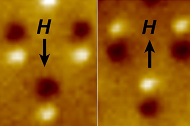
Magnetic microscope image of three nanomagnetic computer bits. Each bit is a tiny bar magnet only 90 nanometers long. The image hows a bright spot at the “North” end and a dark spot at the “South” end of the magnet. The “H” arrow shows the direction of magnetic field applied to switch the direction of the magnets. (credit: Jeongmin Hong et al./Science Advances)

UC Berkeley engineers have shown for the first time that magnetic chips can actually operate at the lowest fundamental energy dissipation theoretically possible under the laws of thermodynamics. That means dramatic reductions in power consumption are possible — down to as little as one-millionth the amount of energy per operation used by transistors in modern computers.

The findings were published Mar. 11 an open-access paper in the peer-reviewed journal Science Advances.

This is critical at two ends of the size scale: for mobile devices, which demand powerful processors that can run for a day or more on small, lightweight batteries; and on an industrial scale, as computing increasingly moves into “the cloud,” where the electricity demands of the giant cloud data centers are multiplying, collectively taking an increasing share of the country’s — and world’s — electrical grid.

“The biggest challenge in designing computers and, in fact, all our electronics today is reducing their energy consumption,” aid senior author Jeffrey Bokor, a UC Berkeley professor of electrical engineering and computer sciences and a faculty scientist at the Lawrence Berkeley National Laboratory.

Lowering energy use is a relatively recent shift in focus in chip manufacturing after decades of emphasis on packing greater numbers of increasingly tiny and faster transistors onto chips to keep up with Moore’s law.

“Making transistors go faster was requiring too much energy,” said Bokor, who is also the deputy director the Center for Energy Efficient Electronics Science, a Science and Technology Center at UC Berkeley funded by the National Science Foundation. “The chips were getting so hot they’d just melt.”

So researchers have been turning to alternatives to conventional transistors, which currently rely upon the movement of electrons to switch between 0s and 1s. Partly because of electrical resistance, it takes a fair amount of energy to ensure that the signal between the two 0 and 1 states is clear and reliably distinguishable, and this results in excess heat.

Nanomagnetic computing: how low can you get?

The UC Berkeley team used an innovative technique to measure the tiny amount of energy dissipation that resulted when they flipped a nanomagnetic bit. The researchers used a laser probe to carefully follow the direction that the magnet was pointing as an external magnetic field was used to rotate the magnet from “up” to “down” or vice versa.

They determined that it only took 15 millielectron volts of energy — the equivalent of 3 zeptojoules — to flip a magnetic bit at room temperature, effectively demonstrating the Landauer limit (the lowest limit of energy required for a computer operation). *

This is the first time that a practical memory bit could be manipulated and observed under conditions that would allow the Landauer limit to be reached, the authors said. Bokor and his team published a paper in 2011 that said this could theoretically be done, but it had not been demonstrated until now.

While this paper is a proof of principle, he noted that putting such chips into practical production will take more time. But the authors noted in the paper that “the significance of this result is that today’s computers are far from the fundamental limit and that future dramatic reductions in power consumption are possible.”

The National Science Foundation and the U.S. Department of Energy supported this research.

* The Landauer limit was named after IBM Research Lab’s Rolf Landauer, who in 1961 found that in any computer, each single bit operation must expend an absolute minimum amount of energy. Landauer’s discovery is based on the second law of thermodynamics, which states that as any physical system is transformed, going from a state of higher concentration to lower concentration, it gets increasingly disordered. That loss of order is called entropy, and it comes off as waste heat. Landauer developed a formula to calculate this lowest limit of energy required for a computer operation. The result depends on the temperature of the computer; at room temperature, the limit amounts to about 3 zeptojoules, or one-hundredth the energy given up by a single atom when it emits one photon of light.


Abstract of Experimental test of Landauer’s principle in single-bit operations on nanomagnetic memory bits

Minimizing energy dissipation has emerged as the key challenge in continuing to scale the performance of digital computers. The question of whether there exists a fundamental lower limit to the energy required for digital operations is therefore of great interest. A well-known theoretical result put forward by Landauer states that any irreversible single-bit operation on a physical memory element in contact with a heat bath at a temperature Trequires at least kBT ln(2) of heat be dissipated from the memory into the environment, where kB is the Boltzmann constant. We report an experimental investigation of the intrinsic energy loss of an adiabatic single-bit reset operation using nanoscale magnetic memory bits, by far the most ubiquitous digital storage technology in use today. Through sensitive, high-precision magnetometry measurements, we observed that the amount of dissipated energy in this process is consistent (within 2 SDs of experimental uncertainty) with the Landauer limit. This result reinforces the connection between “information thermodynamics” and physical systems and also provides a foundation for the development of practical information processing technologies that approach the fundamental limit of energy dissipation. The significance of the result includes insightful direction for future development of information technology.

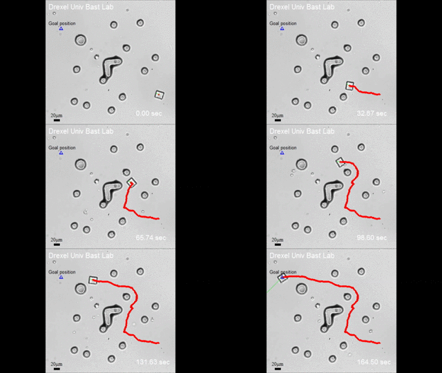
Electrical control of bacteria-powered microrobots

Electric fields help microscopic bacteria-powered robots detect obstacles in their environment and navigate around them to get to their destination. (credit: Drexel University)

Drexel University engineers have developed a method for using electric fields to help microscopic bacteria-powered robots detect obstacles in their environment and navigate around them. Uses include delivering medication, manipulating stem cells to direct their growth, or building a microstructure, for example.

The method is a follow-up to a 2014 report that presented a way to use the flagellated bacteria Serratia marcescens and an electric field to make a microrobot mobile. These bacteria possess a negative charge, which means they can be manipulated, in this case, with two perpendicular electric fields that turn the fluid into an electrified grid.

Serratia marcescens bacteria are the perfect candidate for use in driving microrobots because they have a natural negative charge, which means they can be manipulated with an electric field, and their flagella reduce friction while helping the robot move in a fluid environment. (credit: Drexel University)

By running a series of tests using charged particles, the team realized how the electric field changed when it encountered insulator objects. “The electric field was distorted near the corners of the obstacle,” the authors write. “Particles that passed by the first corner of the obstacles also had affected trajectories even though they had a clear space ahead to pass; this is due to the distorted electric field.”

They used this deformation in the field as input data for their steering algorithm; the robots are using electric fields both as a mode of transportation and as a means of navigation. The algorithm also uses image-tracking from a microscope-mounted camera to locate the initial starting point of the robot and its ultimate destination.

“With this level of control and input from the environment we can program the microrobot to make a series of value judgments during its journey that affect its path,” said MinJun Kim, PhD, a professor in the College of Engineering and director of Drexel’s Biological Actuation, Sensing & Transport (BAST) Lab. “If, for instance, we want the robot to avoid as many obstacles as possible, regardless of the distance traveled. Or we could set it to take the most direct, shortest route to the destination — even if it’s through the obstacles.”

The next step for Kim’s lab is to develop a system consisting of multiple bacteria-powered microrobots that can manipulate multiple live cells in vitro.

The research was recently published in IEEE Transactions on Robotics.


Abstract of Electric Field Control of Bacteria-Powered Microrobots Using a Static Obstacle Avoidance Algorithm

A bacteria-powered microrobot (BPM) is a hybrid robotic system consisting of an SU-8 microstructure with active surfaces or bacterial carpets, in which massive arrays of biomolecular flagellar motors work cooperatively. This paper suggests an obstacle-avoidance method based on a BPM’s response to electric fields. The negatively charged bacteria enable the BPM to follow electric fields. In our previous demonstration of the single BPM controllability, we observed a vast change in the control dynamics when obstructions distorted the applied electric field and affected BPM steering and control. In this paper, we demonstrate an obstacle avoidance method that takes the electric field distortion into account to navigate a BPM through multiple static obstacles in real time. We used an artificial potential field and configuration space in our algorithm to generate an objective function for the electric field distortion and collision around/with obstacles, respectively. In addition, finite-element modeling through COMSOL Multiphysics engineering software was used to simulate charged-particle trajectories in a distorted electric field. Finally, we describe the feasibility of our proposed obstacle avoidance approach through experiments and compared these data with simulation results.

Using machine learning to rationally design future electronics materials

A schematic diagram of machine learning for materials discovery (credit: Chiho Kim, Ramprasad Lab, UConn)

Replacing inefficient experimentation, UConn researchers have used machine learning to systematically scan millions of theoretical compounds for qualities that would make better materials for solar cells, fibers, and computer chips.

Led by UConn materials scientist Ramamurthy ‘Rampi’ Ramprasad, the researchers set out to determine which polymer atomic configurations make a given polymer a good electrical conductor or insulator, for example.

A polymer is a large molecule made of many repeating building blocks. The most familiar example is plastics. What controls a polymer’s properties is mainly how the atoms in the polymer connect to each other. Polymers can also have diverse electronic properties. For example, they can be very good insulators or good conductors. And what controls all these properties is mainly how the atoms in the polymer connect to each other.

But with at least 95 stable elements, the number of possible combinations is astronomical. So they pared down the problem to a manageable subset. Many polymers are made of building blocks containing just a few atoms. They look like this:

Polyurea, a common plastic. In this diagram, N is nitrogen, H hydrogen, and O oxygen. R stands in for any number of chemicals that could slightly alter the polymer, but the repeating NH-O-NH-O is the basic structure. Most polymers look like that, made of carbon (C), H, N and O, with a few other elements thrown in occasionally. (credit: Yikrazuul/public domain)

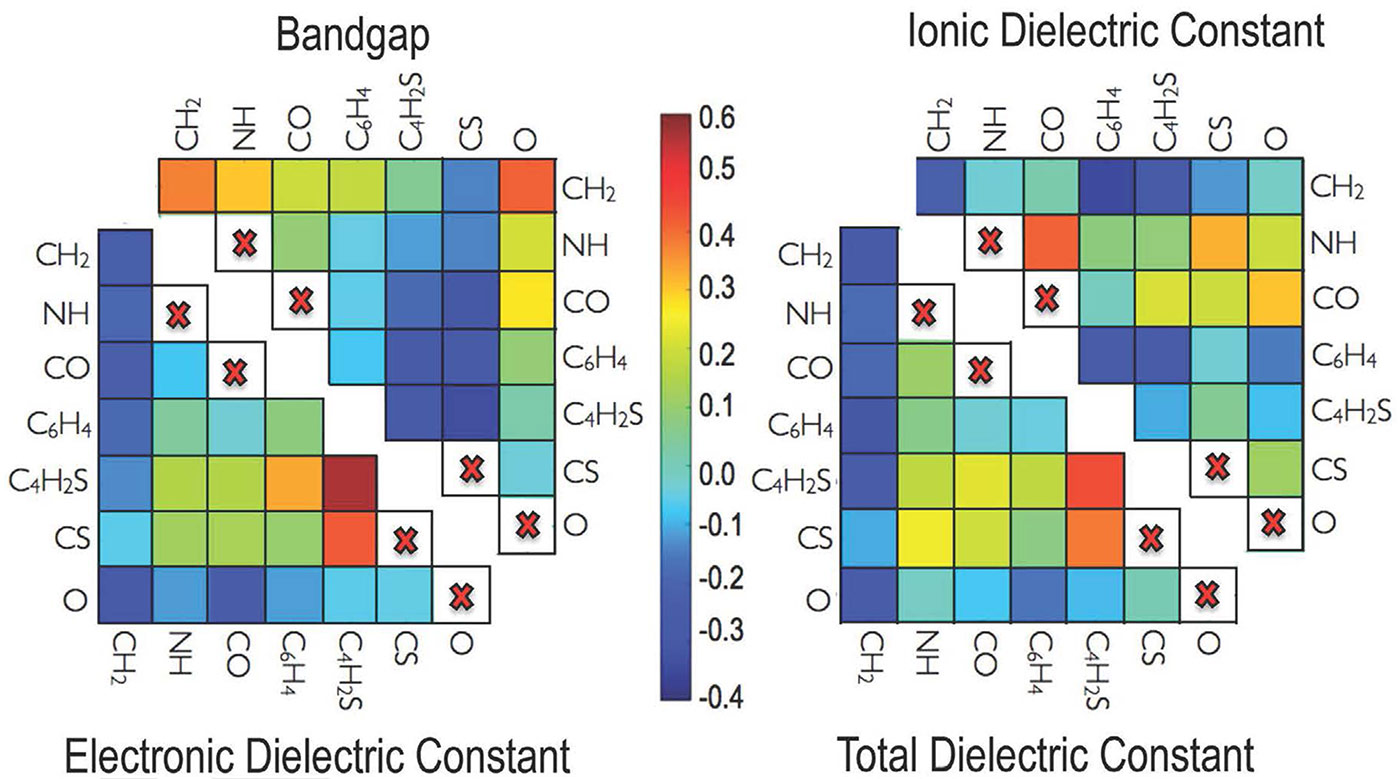
For their project, Ramprasad’s group looked at polymers made of just seven building blocks: CH2, C6H4, CO, O, NH, CS, and C4H2S. These are found in common plastics such as polyethylene, polyesters, and polyureas. An enormous variety of polymers could theoretically be constructed using just these building blocks; Ramprasad’s group decided at first to analyze just 283, each composed of a repeated four-block unit.

They started from basic quantum mechanics, and calculated the three-dimensional atomic and electronic structures of each of those 283 four-block polymers (calculating the position of every electron and atom in a molecule with more than two atoms takes a powerful computer a significant chunk of time, which is why they did it for only 283 molecules).

Calculating key electronic properties

(credit: UConn)

Once they had the three-dimensional structures, they could calculate what they really wanted to know: each polymer’s properties.

  1. Ramprasad’s group calculated the band gap, which is the amount of energy it takes for an electron in the polymer to break free of its home atom and travel around the material; and the dielectric constant, which is a measure of the effect an electric field can have on the polymer. These properties translate to how much electric energy each polymer can store in itself.
  2. They then defined each polymer as a string of numbers, a sort of numerical fingerprint. Since there are seven possible building blocks, there are seven possible numbers, each indicating how many of each block type are contained in that polymer.
  3. But a simple number string like that doesn’t give enough information about the polymer’s structure, so they added a second string of numbers that tell how many pairs there are of each combination of building blocks, such as NH-O or C6H4-CS.
  4. Then they added a third string that described how many triples, like NH-O-CH2, there were. They arranged these strings as a three-dimensional matrix, which is a convenient way to describe such strings of numbers in a computer.
  5. Then they let the computer go to work. Using the library of 283 polymers they had laboriously calculated using quantum mechanics, the machine compared each polymer’s numerical fingerprint to its band gap and dielectric constant, and gradually ‘learned’ which building block combinations were associated with which properties. It could even map those properties onto a two-dimensional matrix of the polymer building blocks.
  6. Once the machine learned which atomic building block combinations gave which properties, it could accurately evaluate the band gap and dielectric constant for any polymer made of any combination of those seven building blocks, using just the numerical fingerprint of its structure.

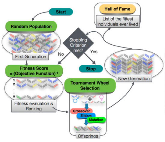
Flow chart of the steps involved in the genetic algorithm (GA) approach, leading to direct design of polymers (credit: Arun Mannodi-Kanakkithodi et al/Scientific Reports)

Validating predictions

Many of the predictions of quantum mechanics and the machine learning scheme have been validated by Ramprasad’s UConn collaborators, who actually made several of the novel polymers and tested their properties.

The group published a paper on their polymer work in an open-access paper in Scientific Reports on Feb. 15; and another paper that utilizes machine learning in a different manner, namely, to discover laws that govern dielectric breakdown of insulators, will be published in a forthcoming issue of Chemistry of Materials.

You can see the predicted properties of every polymer Ramprasad’s group has evaluated in their online data vault, Khazana, which also provides their machine learning apps to predict polymer properties on the fly. They are also uploading data and the machine learning tools from their Chemistry of Materials work, and from an additional recent article published in Scientific Reports on Jan. 19 on predicting the band gap of perovskites, inorganic compounds used in solar cells, lasers, and light-emitting diodes.

Ramprasad’s work is aligned with a larger U.S. White House initiative called the Materials Genome Initiative. Much of Ramprasad’s work described here was funded by grants from the Office of Naval Research, as well as from the U.S. Department of Energy.


Abstract of Machine Learning Strategy for Accelerated Design of Polymer Dielectrics

The ability to efficiently design new and advanced dielectric polymers is hampered by the lack of sufficient, reliable data on wide polymer chemical spaces, and the difficulty of generating such data given time and computational/experimental constraints. Here, we address the issue of accelerating polymer dielectrics design by extracting learning models from data generated by accurate state-of-the-art first principles computations for polymers occupying an important part of the chemical subspace. The polymers are ‘fingerprinted’ as simple, easily attainable numerical representations, which are mapped to the properties of interest using a machine learning algorithm to develop an on-demand property prediction model. Further, a genetic algorithm is utilised to optimise polymer constituent blocks in an evolutionary manner, thus directly leading to the design of polymers with given target properties. While this philosophy of learning to make instant predictions and design is demonstrated here for the example of polymer dielectrics, it is equally applicable to other classes of materials as well.

Are you ready for soft, morphing, crawling robots with glowing skin displays?

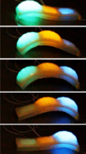
Multi-pixel electroluminescent displays in various states of deformation and illumination (credit: C. Larson et al./Science)

Your future robot or mobile device could have soft, morphable, stretchable “skin” that displays information, according to research by Cornell University engineers. Imagine a health-care robot that displays your blood glucose level and oxygenation, and even your mood — perhaps also your remote physician’s face in 3D.

“When robots become more and more a part of our lives, the ability for them to have an emotional connection with us will be important,” says research team leader Rob Shepherd, an assistant professor of mechanical and aerospace engineering.

Soft robots are currently in use for safe human robot interaction, but they can’t stretch continuously or dynamically display information on their body; and in most cases, can’t sense external and internal stimuli. So the engineers have developed octopus-inspired electroluminescent “skin” that stretches to more than six times its original size, and can also change shape and color.

An undulating gait produced by pressurizing the chambers in sequence along the length of the crawler (credit: C. Larson et al./Science)

The new technology uses a “hyper-elastic light-emitting capacitor” (HLEC), consisting of layers of transparent hydrogel electrodes sandwiching an insulating elastomer (a polymer with viscoelasticity, meaning it has both viscosity and elasticity) sheet.

The elastomer changes luminance and capacitance (the ability to store an electrical charge) when stretched, rolled, and otherwise deformed.

The HLEC skin also endows soft robots with the ability to sense their actuated state and environment and communicate optically — and (for small robots) even crawl.

The engineers created a prototype crawling soft robot, using three of the six-layer HLEC panels bound together. The top four layers made up the illuminated skin and the bottom two served as pneumatic actuators. The chambers were alternately inflated and deflated; the resulting curvature created an undulating, walking motion.

It could also make for a fun pet, we’re guessing.

The team’s research was published in the March 3 online edition of the journal Science. It was supported by a grant from the Army Research Office, a 2015 award from the Air Force Office of Scientific Research, and two grants from the National Science Foundation.

Cornell University | Electroluminescent Skin Demonstration


Abstract of Highly stretchable electroluminescent skin for optical signaling and tactile sensing

Cephalopods such as octopuses have a combination of a stretchable skin and color-tuning organs to control both posture and color for visual communication and disguise. We present an electroluminescent material that is capable of large uniaxial stretching and surface area changes while actively emitting light. Layers of transparent hydrogel electrodes sandwich a ZnS phosphor-doped dielectric elastomer layer, creating thin rubber sheets that change illuminance and capacitance under deformation. Arrays of individually controllable pixels in thin rubber sheets were fabricated using replica molding and were subjected to stretching, folding, and rolling to demonstrate their use as stretchable displays. These sheets were then integrated into the skin of a soft robot, providing it with dynamic coloration and sensory feedback from external and internal stimuli.

Amputee feels texture with a ‘bionic’ fingertip

An amputee feels texture in real time: Signals from sensors in an artificial fingertip are converted to neural-like spikes and delivered to nerves in the upper arm. (credit: Ecole polytechnique fédérale de Lausanne)

Amputee Dennis Aabo Sørensen is the first person in the world to recognize texture (smoothness vs. roughness) using an artificial “bionic” fingertip surgically connected to nerves in his upper arm. The experimental system was developed by EPFL (Ecole polytechnique fédérale de Lausanne) and SSSA (Scuola Superiore Sant’Anna).

“The stimulation felt almost like what I would feel with my hand,” says Sørensen. “I felt the texture sensations at the tip of the index finger of my phantom hand.”

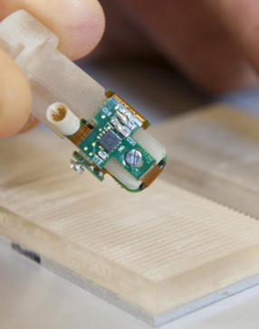
Bionic fingertip electronics and plastic gratings with rough and smooth textures (credit: Hillary Sanctuary/EPFL)

As a test, a machine controlled the movement of the fingertip over different pieces of plastic engraved with different patterns, smooth or rough, as sensors generated an electrical signal. This signal was translated into a series of electrical spikes, imitating the language of the nervous system, then delivered to the nerves.

But how does this sensation relate to the feeling of touch from a real finger? The scientists tested that by comparing brain-wave activity of amputees to non-amputees. The brain scans were similar.

“This study provides additional evidence that research in neuroprosthetics can contribute to [understanding] neuronal mechanisms of the human sense of touch,” says Calogero Oddo of the BioRobotics Institute of SSSA. “It will also be translated to other applications, such as artificial touch in robotics for surgery, rescue, and manufacturing.”

The research is described in an open-access paper on the journal e-Life. It was carried out in collaboration with Università di Pisa, IRCCS San Raffaele Pisana, Università Cattolica del Sacro Cuore, and Università Campus Biomedico.

The work was partly supported by EU Grants TIME, NEBIAS and NANOBIOTOUCH; by the ENABLE project, funded by the Wyss Center for Bio and Neuroengineering; by the Swiss National Competence Center in Research in Robotics; and by Italian grants NEMESIS (funded by the Italian Ministry of Health), PRIN/HandBot (funded by the Italian Ministry of Research), and PPR2 (funded by the National Institute for Insurance against Industrial Injuries).


Abstract of Intraneural stimulation elicits discrimination of textural features by artificial fingertip in intact and amputee humans

Restoration of touch after hand amputation is a desirable feature of ideal prostheses. Here, we show that texture discrimination can be artificially provided in human subjects by implementing a neuromorphic real-time mechano-neuro-transduction (MNT), which emulates to some extent the firing dynamics of SA1 cutaneous afferents. The MNT process was used to modulate the temporal pattern of electrical spikes delivered to the human median nerve via percutaneous microstimulation in four intact subjects and via implanted intrafascicular stimulation in one transradial amputee. Both approaches allowed the subjects to reliably discriminate spatial coarseness of surfaces as confirmed also by a hybrid neural model of the median nerve. Moreover, MNT-evoked EEG activity showed physiologically plausible responses that were superimposable in time and topography to the ones elicited by a natural mechanical tactile stimulation. These findings can open up novel opportunities for sensory restoration in the next generation of neuro-prosthetic hands.

The technology to deliver this sophisticated tactile information was developed by Silvestro Micera and his team at  together with Calogero Oddo and his team at SSSA.

Stretchable, flexible ‘meta-skin’ cloaks objects from radar at a range of frequencies

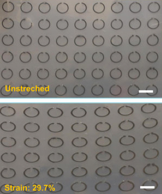
Flexible, stretchable, and frequency-tunable “meta-skin” can trap radar waves and cloak objects from radar detection (scale bars: 5 mm) (credit: Siming Yang et al./Scientific Reports)

Iowa State University engineers have developed a new flexible, stretchable, and  tunable “meta-skin” (metamaterial) “invisibility cloak” that uses rows of small liquid-metal devices to cloak an object from radar over a wide range of frequencies — and possibly at visible or infrared light ranges in the future.

First wraparound meta-skin (credit: Siming Yang et al./Scientific Reports)

The  skin has rows of split ring resonators embedded inside layers of silicone sheets. The resonators are filled with galinstan, a metal alloy that’s liquid at room temperature. That allows for stretching and flexing the polymer meta-skin, enabling it to be tuned to reduce reflection at a wide range of radar frequencies, unlike previous metamaterials.

Applications could include sub-wavelength imaging (of smaller objects), electromagnetic frequency tuning, shielding (from interference or detection), and scattering suppression (allowing a signal to be sent in specific directions rather than scattered).

Unlike conventional metamaterials, meta-skin can be conformed to curved and irregular surfaces.

The split-ring resonators used here are small rings with an outer radius of 2.5 millimeters and a thickness of half a millimeter. They have a 1 millimeter gap, essentially creating a small, curved segment of liquid wire.

The rings create electric inductors and the gaps create electric capacitors. Together they create a tuned resonator that can trap and suppress radar waves at a specific frequency. Stretching the meta-skin changes the size of the liquid metal rings inside and lowers the frequency the devices suppress.

Tests showed radar suppression was about 75 percent in the frequency range of 8 to 10 gigahertz in the experiment, according to the paper. When objects are wrapped in the meta-skin, the radar waves were suppressed in all incident directions and observation angles.

The open-access journal Scientific Reports recently reported the discovery online.

“The long-term goal is to shrink the size of these devices,” said senior author and associate professor Liang Dong, allowing for use with higher-frequency electromagnetic waves such as visible or infrared light. That would require advanced nanomanufacturing technologies and appropriate structural modifications, Dong noted.

The National Science Foundation and the China Scholarship Council partially supported the project.


Abstract of From Flexible and Stretchable Meta-Atom to Metamaterial: A Wearable Microwave Meta-Skin with Tunable Frequency Selective and Cloaking Effects

This paper reports a flexible and stretchable metamaterial-based “skin” or meta-skin with tunable frequency selective and cloaking effects in microwave frequency regime. The meta-skin is composed of an array of liquid metallic split ring resonators (SRRs) embedded in a stretchable elastomer. When stretched, the meta-skin performs as a tunable frequency selective surface with a wide resonance frequency tuning range. When wrapped around a curved dielectric material, the meta-skin functions as a flexible “cloaking” surface to significantly suppress scattering from the surface of the dielectric material along different directions. We studied frequency responses of multilayer meta-skins to stretching in a planar direction and to changing the spacing between neighboring layers in vertical direction. We also investigated scattering suppression effect of the meta-skin coated on a finite-length dielectric rod in free space. This meta-skin technology will benefit many electromagnetic applications, such as frequency tuning, shielding, and scattering suppression.

Stretchable electronics that can quadruple in length

Stretchable biphasic gold–gallium thin films. Scale bar: 5 mm; Inset scale bar: 500 micrometers. (credit: Arthur Hirsch et al./Advanced Materials)

EPFL researchers have developed films with conductive tracks just several hundreds of nanometers thick that can be bent and stretched up to four times their original length. They could be used in artificial skin, connected clothing, and on-body sensors.

Instead of bring printed on a board, the tracks are almost as flexible as rubber and can be stretched up to four times their original length and in all directions a million times without cracking or interrupting their conductivity. The material could be used to make circuits that can be twisted and stretched — ideal for artificial skin on prosthetics or robotic machines.

It could also be integrated into fabric and used in connected clothing. And because it follows the shape and movements of the human body, it could be used for sensors designed to monitor particular biological functions.

The films use an alloy of gallium to achieve a liquid state at room temperature and gold to ensures the gallium remains homogeneous, preventing it from separating into droplets. The invention is described in an article published today in the journal Advanced Materials.


École polytechnique fédérale de Lausanne (EPFL) | Stretchable electronics that quadruple in length


Abstract of Intrinsically Stretchable Biphasic (Solid–Liquid) Thin Metal Films

Stretchable biphasic conductors are formed by physical vapor deposition of gallium onto an alloying metal film. The properties of the photolithography-compatible thin metal films are highlighted by low sheet resistance (0.5 Ω sq−1) and large stretchability (400%). This novel approach to deposit and pattern liquid metals enables extremely robust, multilayer and soft circuits, sensors, and actuators.

Better memory through electricity

Transient increase in intracellular calcium ions during tDCS initiates molecular cascades leading to improved memory and brain plasticity* (credit: Maria Vittoria Podda et al./Scientific Reports)

Researchers at Catholic University Medical School in Rome have boosted the memory and mental performance of laboratory mice by transcranial Direct Current Stimulation (tDCS) and identified the molecular trigger for the improvement.

A noninvasive technique for brain stimulation, tDCS is applied using two small electrodes placed on the scalp, delivering short bursts of low-intensity electrical currents.

After exposing the mice to single 20-minute tDCS sessions, the researchers saw signs of improved memory and brain plasticity (the ability to form new connections between neurons when learning new information) in the hippocampus (a region of the brain critical to memory processing and storage), which lasted at least a week.

This boost was demonstrated by the enhanced performance of the mice during tests requiring them to navigate a water maze and distinguish between known and unknown objects.

Molecular trigger identified

The researchers also identified the molecular trigger behind the bolstered memory and plasticity: increased production of brain-derived neurotrophic factor (BDNF), a protein essential to brain growth that is synthesized naturally by neurons and is crucial to neuronal development and specialization.

The study was published in Nature Scientific Reports and sponsored by the Office of Naval Research (ONR) Global.

“In addition to potentially enhancing task performance for Sailors and Marines,” said ONR Global Commanding Officer Capt. Clark Troyer, “understanding how this technique works biochemically may lead to advances in the treatment of conditions like post-traumatic stress disorder, depression, and anxiety, which affect learning and memory in otherwise healthy individuals.”

The research may also have potential to strengthen learning and memory in both healthy people and those with cognitive deficits such as Alzheimer’s. “We already have promising results in animal models of Alzheimer’s disease,” said Claudio Grassi, PhD., who leads the research team.

Although tDCS has been used for years to treat patients suffering from conditions such as stroke, depression and bipolar disorder, there are few studies supporting a direct link between tDCS and improved plasticity, making Grassi’s work unique.

* Transient increase in intracellular Ca2+ during tDCS initiates molecular cascades leading to persistent changes in chromatin structure of brain-derived neurotrophic factor (BDNF). These include the phosphorylation of CREB, its binding to BDNF promoter I and recruitment of CREB/CREB-binding protein (CBP). CBP, in turn, promotes H3 acetylation at lysine 9 (H3K9ac) acetylation of BDNF (specifically at promoter I). As a result, stimuli such as long-term potentiation (LTP) induction protocol in slices or learning and memory in vivo are more effective in promoting transcription of BDNF previously primed by anodal tDCS.


Abstract of Anodal transcranial direct current stimulation boosts synaptic plasticity and memory in mice via epigenetic regulation of Bdnf expression

The effects of transcranial direct current stimulation (tDCS) on brain functions and the underlying molecular mechanisms are yet largely unknown. Here we report that mice subjected to 20-min anodal tDCS exhibited one-week lasting increases in hippocampal LTP, learning and memory. These effects were associated with enhanced: i) acetylation of brain-derived neurotrophic factor (Bdnf) promoter I; ii) expression of Bdnfexons I and IX; iii) Bdnf protein levels. The hippocampi of stimulated mice also exhibited enhanced CREB phosphorylation, pCREB binding to Bdnf promoter I and recruitment of CBP on the same regulatory sequence. Inhibition of acetylation and blockade of TrkB receptors hindered tDCS effects at molecular, electrophysiological and behavioral levels. Collectively, our findings suggest that anodal tDCS increases hippocampal LTP and memory via chromatin remodeling of Bdnf regulatory sequences leading to increased expression of this gene, and support the therapeutic potential of tDCS for brain diseases associated with impaired neuroplasticity.

‘Fingerprinting’ and neural nets could help protect power grid, other industrial systems

Electrical substation (credit: Fitrah Hamid, Georgia Tech)

Georgia Tech researchers have developed a device fingerprinting technique that could improve the security of the electrical grid and other industrial systems.

“The stakes are extremely high; the systems are very different from home or office computer networks,” said Raheem Beyah, an associate professor in the School of Electrical and Computer Engineering at the Georgia Institute of Technology.

The networked systems controlling the U.S. electrical grid and other industrial systems, carried out over supervisory control and data acquisition (SCADA) protocols, often lack the ability to run modern encryption and authentication systems. The legacy systems connected to them were never designed for networked security, Beyah said. Because they are distributed around the country, often in remote areas, the systems are also difficult to update using the “patching” techniques common in computer networks.

Fingerprinting to detect false data or commands

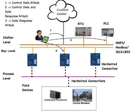
Points of attack in a power substation network (credit: David Formby et al./Network and Distributed System Security Symposium)

Which is why Beyah and his team have developed “fingerprinting techniques” to protect various operations of the power grid to prevent or minimize spoofing of packets that could be injected to produce false data or false control commands into the system. “This is the first technique that can passively fingerprint different devices that are part of critical infrastructure networks,” he said. “We believe it can be used to significantly improve the security of the grid and other networks.”

For instance, control devices used in the power grid produce signals that are distinctive because of their unique physical configurations and compositions. Security devices listening to signals traversing the grid’s control systems can differentiate between these legitimate devices and signals produced by equipment that’s not part of the system.

Devices such as circuit breakers and electrical protection systems can also be told to open or close remotely, and they then report on the actions they’ve taken. The time required to open a breaker or a valve is determined by the physical properties of the device. If an acknowledgement arrives too soon after the command is issued — less time than it would take for a breaker or valve to open, for instance — the security system could suspect spoofing, Beyah explained.

To develop the device fingerprints, the researchers have built computer models of utility grid devices to understand how they operate. Information to build the models came from “black box” techniques — watching the information that goes into and out of the system — and “white box” techniques using schematics or physical access to the systems and unique signatures that indicates the identity of specific devices, or device type, or associated actions.

The researchers used supervised learning techniques when a list of IP addresses and corresponding device types were available; and unsupervised learning when not available, with performance nearly as high as the supervised learning methods.

The researchers have demonstrated the technique on two electrical substations, and plan to continue refining it until it becomes close to 100 percent accurate. Their current technique addresses the protocol used for more than half of the devices on the electrical grid, and future work will include examining application of the method to other protocols.

Other vulnerable systems

Beyah believes the approach could have broad application to securing industrial control systems used in manufacturing, oil and gas refining, wastewater treatment and other industries where they use devices with measurable physical properties. Beyond industrial controls, the principle could also apply to the Internet of Things (IoT), where the devices being controlled have specific signatures related to switching them on and off.

“All of these IoT devices will be doing physical things, such as turning your air-conditioning on or off,” Beyah said. “There will be a physical action occurring, which is similar to what we have studied with valves and actuators.”

The research, reported February 23 at the Network and Distributed System Security Symposium in San Diego, was supported in part by the National Science Foundation (NSF). The approach has been successfully tested in two electrical substations.


Abstract of Who’s in Control of Your Control System? Device Fingerprinting for Cyber-Physical Systems

Industrial control system (ICS) networks used in critical infrastructures such as the power grid present a unique set of security challenges. The distributed networks are difficult to physically secure, legacy equipment can make cryptography and regular patches virtually impossible, and compromises can result in catastrophic physical damage. To address these concerns, this research proposes two device type fingerprinting methods designed to augment existing intrusion detection methods in the ICS environment. The first method measures data response processing times and takes advantage of the static and low-latency nature of dedicated ICS networks to develop accurate fingerprints, while the second method uses the physical operation times to develop a unique signature for each device type. Additionally, the physical fingerprinting method is extended to develop a completely new class of fingerprint generation that requires neither prior access to the network nor an example target device. Fingerprint classification accuracy is evaluated using a combination of a real world five month dataset from a live power substation and controlled lab experiments. Finally, simple forgery attempts are launched against the methods to investigate their strength under attack.

Quantum dot solids: a new era in electronics?

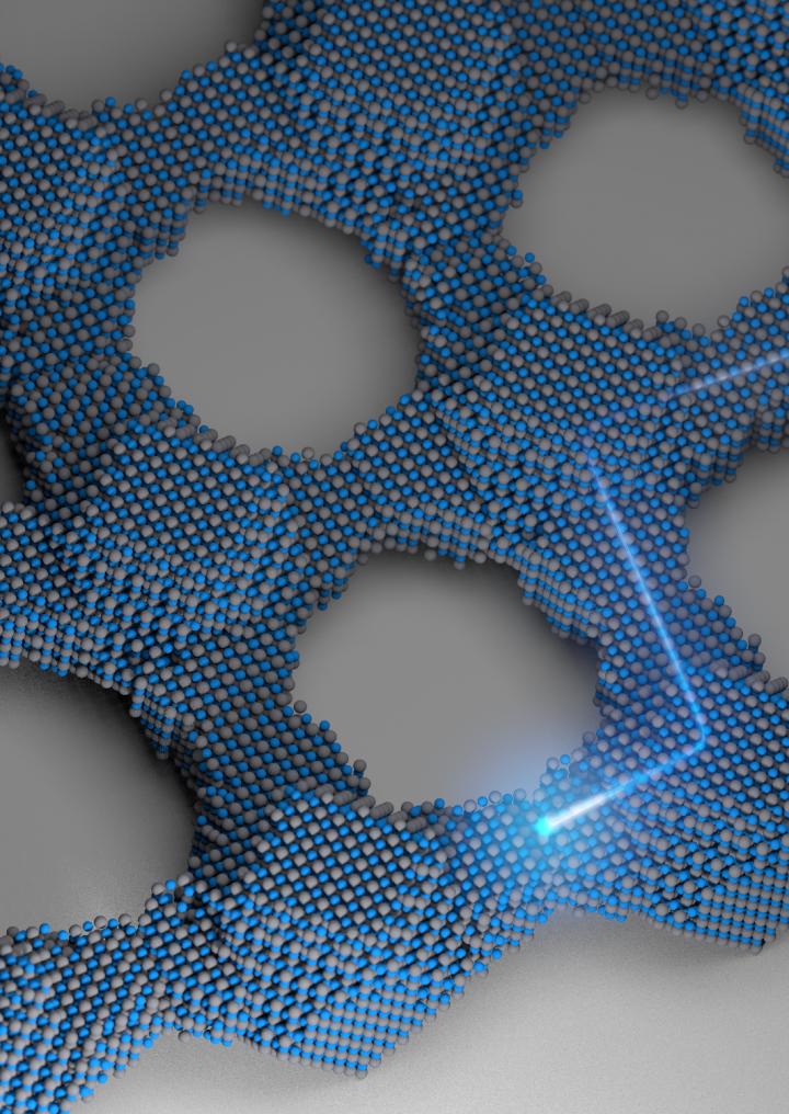
Connecting the dots: Playing ‘LEGO’ at the atomic scale to build atomically coherent quantum dot solids (credit: Kevin Whitham, Cornell University)

Just as the single-crystal silicon wafer forever changed the nature of communication 60 years ago, Cornell researchers hope their work with quantum dot solids — crystals made out of crystals — can help usher in a new era in electronics.

The team has fashioned two-dimensional superstructures out of single-crystal building blocks. Using a pair of chemical processes, the lead-selenium nanocrystals are synthesized into larger crystals, then fused together to form atomically coherent square superlattices.


Cornell University | Quantum dot solids

The difference between these and previous crystalline structures is the atomic coherence of each 5-nanometer crystal (a nanometer is one-billionth of a meter). They’re not connected by a substance between each crystal — they’re connected to each other directly. The electrical properties of these superstructures are potentially superior to existing semiconductor nanocrystals, with anticipated applications in energy absorption and light emission.

“As far as level of perfection, in terms of making the building blocks and connecting them into these superstructures, that is probably as far as you can push it,” said Tobias Hanrath, associate professor in the Robert Frederick Smith School of Chemical and Biomolecular Engineering, referring to the atomic-scale precision of the process.

The Hanrath group’s paper, “Charge transport and localization in atomically coherent quantum dot solids,” is published in this month’s issue of Nature Materials.

The strong coupling of the nanocrystals leads to formation of energy bands that can be manipulated based on the crystals’ makeup, and could be the first step toward discovering and developing other artificial materials with controllable electronic structure.

The structure of the Hanrath group’s superlattice, while superior to ligand-connected nanocrystal solids, still has multiple sources of disorder due to the fact that all nanocrystals are not identical. This creates defects, which limit electron wave function.

This work made use of the Cornell Center for Materials Research, which is supported by the National Science Foundation through its Materials Research Science and Engineering Center program. X-ray scattering was conducted at the Cornell High Energy Synchrotron Source, which is supported by the NSF and the National Institutes of Health.


Abstract of Charge transport and localization in atomically coherent quantum dot solids

Epitaxial attachment of quantum dots into ordered superlattices enables the synthesis of quasi-two-dimensional materials that theoretically exhibit features such as Dirac cones and topological states, and have major potential for unprecedented optoelectronic devices. Initial studies found that disorder in these structures causes localization of electrons within a few lattice constants, and highlight the critical need for precise structural characterization and systematic assessment of the effects of disorder on transport. Here we fabricated superlattices with the quantum dots registered to within a single atomic bond length (limited by the polydispersity of the quantum dot building blocks), but missing a fraction (20%) of the epitaxial connections. Calculations of the electronic structure including the measured disorder account for the electron localization inferred from transport measurements. The calculations also show that improvement of the epitaxial connections will lead to completely delocalized electrons and may enable the observation of the remarkable properties predicted for these materials.