UCSD spinoffs create lab-quality portable 64-channel BCI headset

A dry-electrode, portable 64-channel wearable EEG headset (credit: Jacobs School of Engineering/UC San Diego)

The first dry-electrode, portable 64-channel wearable brain-computer interface (BCI) has been developed by bioengineers and cognitive scientists associated with UCSD Jacobs School.

The system is comparable to state-of-the-art equipment found in research laboratories, but with portability, allowing for tracking brain states throughout the day and augmenting the brain’s capabilities, the researchers say. Current BCI devices require gel-based electrodes or fewer than 64 channels.

The dry EEG sensors are easier to apply than wet sensors, while still providing high-density/low-noise brain activity data, according to the researchers. The headset includes a Bluetooth transmitter, eliminating the usual array of wires. The system also includes a sophisticated software suite for data interpretation and analysis for applications including research, neuro-feedback, and clinical diagnostics.
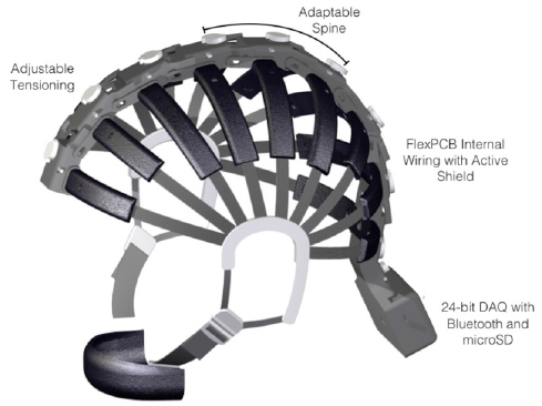
Cognionics HD-72 64-channel mobile EEG system (credit: Cognionics)

“This is going to take neuroimaging to the next level by deploying on a much larger scale,” including use in homes and even while driving, said Mike Yu Chi, a Jacobs School alumnus and CTO of Cognionics who led the team that developed the headset.

The researchers also envision a future when neuroimaging can be used to bring about new therapies for neurological disorders. “We will be able to prompt the brain to fix its own problems,” said Gert Cauwenberghs, a bioengineering professor at the Jacobs School and a principal investigator on a National Science Foundation grant. “We are trying to get away from invasive technologies, such as deep brain stimulation and prescription medications, and instead start up a repair process by using the brain’s synaptic plasticity.”

“In 10 years, using a brain-machine interface might become as natural as using your smartphone is today, said Tim Mullen, a UC San Diego alumnus, lead author on the study and a former researcher at the Swartz Center for Computational Neuroscience at UC San Diego.

The researchers from the Jacobs School of Engineering and Institute for Neural Computation at UC San Diego detailed their findings in an article of the Special Issue on Wearable Technologies published recently in IEEE Transactions on Biomedical Engineering.

EEG headset
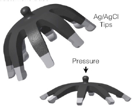
The innovative dry electrodes developed by the researchers eliminate the complexity and mess of affixing gel electrodes. By using silver/silver chloride tips, along with associated electronics and special headset mechanical construction, the dry electrodes reduce electrical noise and can be conveniently used through hair. (credit: Tim R. Mullen et al./IEEE Transactions on Biomedical Engineering)

For this vision of the future to become a reality, sensors will need to become not only wearable but also comfortable, and algorithms for data analysis will need to be able to cut through noise to extract meaningful data. The EEG headset developed by Chi and his team has an octopus-like shape, in which each arm is elastic, so that it fits on many different kinds of head shapes. The sensors at the end of each arm are designed to make optimal contact with the scalp while adding as little noise in the signal as possible.

The researchers spent four years perfecting the sensors’ materials. The sensors are designed to work on a subject’s hair. The material allows the sensors to remain flexible and durable while still conducting high-quality signals, thanks to a silver/silver-chloride coating. The design includes shielding from interference from electrical equipment and other electronics. The researchers also developed sensors intended for direct application to the scalp.

Software and data analysis

In the study, the data that the headset captured were analyzed with software developed by Mullen and Christian Kothe, another former researcher at the Swartz Center for Computational Neuroscience.

First, brain signals needed to be separated from noise in the EEG data. The tiny electrical currents originating from the brain are often contaminated by high-amplitude artifacts generated when subjects move, speak, or even blink. The researchers designed an algorithm that separates the EEG data in real-time into different components that are statistically unrelated to one another.

The algorithm then compares these elements with clean data obtained, for instance, when a subject is at rest. Abnormal data are labeled as noise and discarded. “The algorithm attempts to remove as much of the noise as possible while preserving as much of the brain signal as possible,” said Mullen.

The researchers were also able to track, in real time, how signals from different areas of the brain interact with one another, building an ever-changing network map of brain activity. They then used machine learning to connect specific network patterns in brain activity to cognition and behavior.

Future plans

Mullen’s start-up, Qusp, has developed NeuroScale, a cloud-based software platform that provides continuous real-time interpretation of brain and body signals through an Internet application program interface (API). The goal is to enable brain-computer interface and advanced signal processing methods to be easily integrated with various everyday applications and wearable devices.

“A Holy Grail in our field is to track meaningful changes in distributed brain networks at the ‘speed of thought’,” Mullen said. “We’re closer to that goal, but we’re not quite there yet.”

Cognionics is selling the headset to research groups, especially for use in neuro-feedback. Next steps include improving the headset’s performance while subjects are moving. The device can reliably capture signals while subjects walk but less so during more strenuous activities such as running. Electronics also need improvement to function for longer time periods — days and even weeks instead of hours.

The ultimate goal is to get the headset into the clinic to help diagnose a range of conditions, such as strokes and seizures, says Chi.

These researchers’ development and testing projects have been funded in part by a five-year Emerging Frontiers of Research Innovation grant from the National Science Foundation, DARPA, and the Army Research Laboratory (Aberdeen, MD) Collaborative Technology Alliance (CTA).


Abstract of Real-time neuroimaging and cognitive monitoring using wearable dry EEG

Goal: We present and evaluate a wearable high-density dry-electrode EEG system and an open-source software framework for online neuroimaging and state classification. Methods: The system integrates a 64-channel dry EEG form factor with wireless data streaming for online analysis. A real-time software framework is applied, including adaptive artifact rejection, cortical source localization, multivariate effective connectivity inference, data visualization, and cognitive state classification from connectivity features using a constrained logistic regression approach (ProxConn). We evaluate the system identification methods on simulated 64-channel EEG data. Then, we evaluate system performance, using ProxConn and a benchmark ERP method, in classifying response errors in nine subjects using the dry EEG system. Results: Simulations yielded high accuracy (AUC = 0.97 ± 0.021) for real-time cortical connectivity estimation. Response error classification using cortical effective connectivity [short-time directdirected transfer function (sdDTF)] was significantly above chance with similar performance (AUC) for cLORETA (0.74 ± 0.09) and LCMV (0.72 ± 0.08) source localization. Cortical ERPbased classification was equivalent to ProxConn for cLORETA (0.74 ± 0.16) butsignificantlybetterforLCMV (0.82 ± 0.12). Conclusion: We demonstrated the feasibility for real-time cortical connectivity analysis and cognitive state classification from highdensity wearable dry EEG. Significance: This paper is the first validated application of these methods to 64-channel dry EEG. This study addresses a need for robust real-time measurement and interpretation of complex brain activity in the dynamic environment of the wearable setting. Such advances can have broad impact in research, medicine, and brain-computer interfaces. The pipelines are made freely available in the open-source SIFT and BCILAB toolboxes.

A battery that shuts down at high temperatures and restarts when it cools

Stanford researchers have developed a thin polyethylene film that prevents a lithium-ion battery from overheating, then restarts the battery when it cools. The film is embedded with spiky nanoparticles of graphene-coated nickel. (credit: Zheng Chen)

Stanford researchers have invented a lithium-ion battery that shuts down before overheating to prevent the battery fires that have plagued laptops, hoverboards and other electronic devices. The battery restarts immediately when the temperature cools.

The design is an enhancement of a wearable sensor that monitors human body temperature invented by Zhenan Bao, a professor of chemical engineering at Stanford. The sensor is made of a plastic material embedded with tiny particles of nickel with nanoscale spikes protruding from their surface. For the battery experiment, the researchers coated the spiky nickel particles with graphene, an atom-thick layer of carbon, and embedded the particles in a thin film of elastic polyethylene.

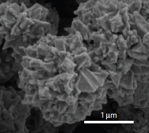
SEM image of conductive spiky graphene-coated nickel nanoparticles (credit: Zheng Chen et al./Nature Energy)

To conduct electricity, the spiky particles have to physically touch one another. But during thermal expansion, polyethylene stretches. That causes the particles to spread apart, making the film non-conductive so that electricity can no longer flow through the battery. When the battery cools, the polyethylene shrinks, bringing the particles in contact again and causing the battery to generate power.

The new battery design has up to 10,000 times higher temperature sensitivity than previous switch devices, and the temperature range can be adjusted by changing the particle density or type of polymer.

“We’ve designed the first battery that can be shut down and revived over repeated heating and cooling cycles without compromising performance,” says Bao. The new battery is described in a study published today (Jan. 11) in the new journal Nature Energy.


Delvon Simmons | My hover board on fire

A typical lithium-ion battery today consists of two electrodes and a liquid or gel electrolyte that carries charged particles between them. Puncturing, shorting or overcharging the battery generates heat. If the temperature reaches about 300 degrees Fahrenheit (150 degrees Celsius), the electrolyte could catch fire and trigger an explosion, as some hoverboard users have recently discovered.

The research was supported by the SLAC National Accelerator Laboratory and the Precourt Institute for Energy at Stanford.

Stanford Precourt Institute for Energy | A lithium-ion battery that shuts down before overheating, then restarts immediately when the temperature cools.


Abstract of  Fast and reversible thermoresponsive polymer switching materials for safer batteries

Safety issues have been a long-standing obstacle impeding large-scale adoption of next-generation high-energy-density batteries. Materials solutions to battery safety management are limited by slow response times and small operating voltage windows. Here we report a fast and reversible thermoresponsive polymer switching material that can be incorporated inside batteries to prevent thermal runaway. This material consists of electrochemically stable graphene-coated spiky nickel nanoparticles mixed in a polymer matrix with a high thermal expansion coefficient. The as-fabricated polymer composite films show high electrical conductivity of up to 50 S per cm at room temperature. Importantly, the conductivity decreases within 1 s by seven to eight orders of magnitude on reaching the transition temperature and spontaneously recovers at room temperature. Batteries with this self-regulating material built in the electrode can rapidly shut down under abnormal conditions such as overheating and shorting, and are able to resume their normal function without performance compromise or detrimental thermal runaway. Our approach offers 1,000–10,000 times higher sensitivity towards temperature changes than previous switching devices.

‘Solar thermal fuel’ polymer film can harvest sunlight by day, release heat on-demand

“Solar thermal fuel” polymer film comprising three distinct layers with tunable thickness (4 to 5 microns for each) (credit: Courtesy of the researchers)

MIT researchers have developed a new transparent polymer film that can store solar energy during the day and release it later as heat, whenever needed. The material could be applied to many different surfaces, such as window glass or clothing.

The new material solves a problem with renewable solar energy: the Sun is not available at night or on stormy days. Most solutions have focused on storing and recovering solar energy as electricity or other forms. The new finding could provide a highly efficient method for storing the sun’s energy through a chemical storage system, which can retain the energy indefinitely in a stable molecular configuration and release it later as heat.

Storing-releasing heat as molecular configurations

The finding, by a research team headed by MIT professor Jeffrey Grossman, is described in a paper in the journal Advanced Energy Materials.

A spin-coating process enables the solar thermal fuel polymer material to deposit from solution. The film can then be readily charged with ultraviolet light. This process can be extended to a variable-thickness layer-by-layer process. (credit: Courtesy of the researchers)

The key is an azobenzene molecule that can remain stable in either of two different configurations: charged and uncharged. When exposed to sunlight, the energy of the light kicks the molecules into their “charged” configuration, and they can stay that way for long periods. Then, when triggered by a very specific temperature or other stimulus, the molecules snap back to their original shape, giving off a burst of heat in the process.

Built-in windshield de-icing

The platform for testing macroscopic heat release. A heating element (bottom) is used to provide sufficient energy to trigger the solar thermal fuel materials, while an infrared camera (yellow circles) monitors the temperature. The charged film (right) releases heat enabling a higher temperature relative to the uncharged film (left). (credit: Courtesy of the researchers)

The “solar thermal fuel” material is highly transparent, which could make it useful for de-icing car windshields, says Grossman, the Morton and Claire Goulder and Family Professor in Environmental Systems and a professor of materials science and engineering.

While many cars already have fine heating wires embedded in rear windows for that purpose, anything that blocks the view through the front window is forbidden by law, even thin wires.

But a transparent film made of the new material, sandwiched between two layers of glass — as is currently done with bonding polymers to prevent pieces of broken glass from flying around in an accident — could provide the same de-icing effect without any blockage. German auto company BMW, a sponsor of this research, is interested in that potential application, Grossman says.

With such a window, energy would be stored in the polymer every time the car sits out in the sunlight. Then, “when you trigger it,” using just a small amount of heat that could be provided by a heating wire or puff of heated air, “you get this blast of heat,” Grossman says.

“We did tests to show you could get enough heat to drop ice off a windshield.” Accomplishing that, he explains, doesn’t require that all the ice actually be melted, just that the ice closest to the glass melts enough to provide a layer of water that releases the rest of the ice to slide off by gravity or be pushed aside by the windshield wipers.

The team is continuing to work on improving the film’s properties, Grossman says, improving its transparency and temperature increase (from 10 degrees Celsius above the surrounding temperature — sufficient for the ice-melting application — to 20 degrees). The new polymer could also significantly reduce electrical drain for heating and de-icing in electric cars, he says.

The work was supported by a NSERC Canada Banting Fellowship and by BMW.


Abstract of Solid-State Solar Thermal Fuels for Heat Release Applications

Closed cycle systems offer an opportunity for solar energy harvesting and storage all within the same material. Photon energy is stored within the chemical conformations of molecules and is retrieved by a triggered release in the form of heat. Until now, such solar thermal fuels (STFs) have been largely unavailable in the solid-state, which would enable them to be utilized for a multitude of applications. A polymer STF storage platform is synthesized employing STFs in the solid-state. This approach enables uniform films capable of appreciable heat storage of up to 30 Wh kg−1 and that can withstand temperature of up to 180 °C. For the first time a macroscopic energy release is demonstrated using spatial infrared heat maps with up to a 10 °C temperature change. These findings pave the way for developing highly efficient and high energy density STFs for applications in the solid-state.

An 18-inch video display you can roll up like a newspaper

(credit: LG)

LG is creating a buzz at CES with its concept demo of the world’s first display that can be rolled up like a newspaper.

LG says they’re aiming for 4K-quality 55-inch screens (the prototype resolution is 1,200 by 810 pixels), BBC reports.

The trick:  switching from LED to thinner, more-flexible OLED technology (organic light-emitting diodes), allowing for a 2.57 millimeter-thin display. One limitation: the screen can’t be flattened.

What this design might be useful for in the future is not clear, but experts suggest the technology could soon be used on smartphones and in-car screens that curve around a vehicle’s interior, Daily Mail notes.

LG is also displaying a 55-inch double-sided display that’s as thin as a piece of paper and shows different video images on each side, and two 65-inch “extreme-curve” TVs that bend inwards and outwards.

CNET CES Videos

Optoelectronic microprocessors shown to dramatically reduce chips’ power consumption

Researchers have produced a working optoelectronic chip that computes electronically but uses light to move information. The chip has 850 optical components and 70 million transistors, which, while significantly less than the billion-odd transistors of a typical microprocessor, is enough to demonstrate all the functionality that a commercial optical chip would require. (credit: Glenn J. Asakawa)

Rsearchers at MIT, the University of California at Berkeley, and the University of Colorado have produced a working optoelectronic microprocessor, which computes electronically but uses light to move information — using only processes found in existing microchip fabrication facilities.

Optical communication could dramatically reduce chips’ power consumption, which is essential to maintaining the steady increases in computing power that we’ve come to expect.

Demonstrating that optical chips can be built with no alteration to existing semiconductor manufacturing processes should make optical communication more attractive to the computer industry. But it also makes an already daunting engineering challenge even more difficult.

“You have to use new physics and new designs to figure out how you take ingredients and process recipes that are used to make transistors, and use those to make photodetectors, light modulators, waveguides, optical filters, and optical interfaces,” says MIT professor of electrical engineering Rajeev Ram, referring to the optical components necessary to encode data onto different wavelengths of light, transmit it across a chip, and then decode it.

Powering down

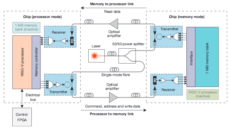
Block diagram of the optical memory system. The system uses one chip acting as the processor and the other acting as memory, connected by a full-duplex optical link with a round-trip distance of 20 m by fiber. PD, photodetector.

The chip has 850 optical components and 70 million transistors, which, while significantly less than the billion-odd transistors of a typical microprocessor, is enough to demonstrate all the functionality that a commercial optical chip would require. In tests, the researchers found that the performance of their transistors was virtually indistinguishable from that of all-electronic computing devices built in the same facility.*

Computer chips are constantly shipping data back and forth between logic circuits and memory, and today’s chips cannot keep the logic circuits supplied with enough data to take advantage of their ever-increasing speed. Boosting the bandwidth of the electrical connections between logic and memory would require more power, and that would raise the chips’ operating temperatures to unsustainable levels.

Optical data connections are, in principle, much more energy efficient. And unlike electrical connections, their power requirements don’t increase dramatically with distance. So optical connections could link processors that were meters rather than micrometers apart, with little loss in performance.

The new paper “certainly is an important result,” says Jagdeep Shah, a researcher at the U.S. Department of Defense’s Institute for Defense Analyses who, as a program director at the Defense Advanced Research Project Agency, initiated the program that sponsored the researchers’ work. “It is not at the megascale yet, and there are steps that need to be taken in order to get there. But this is a good step in that direction.”

“I think that the [chipmaker] GlobalFoundries process was an industry-standard 45-nanometer design-rule process,” Shah adds. “I don’t think that there need be any concern that there’s any foundry that can’t make these things.”

The paper in Nature describing the new chip has 22 co-authors.

* One of the difficulties in using transistor-manufacturing processes to produce optical devices is that transistor components are intended to conduct electricity, at least some of the time. But conductivity requires free charge carriers, which tend to absorb light particles, limiting optical transmission.

Computer chips, however, generally use both negative charge carriers — electrons — and positive charge carriers — “holes,” or the absence of an electron where one would be expected. “That means that somewhere in there, there should be some way to block every kind of [carrier] implant that they’re doing for every layer,” Ram explains. “We just had to figure out how we do that.”

In an optoelectronic chip, at some point, light signals have to be converted to electricity. But contact with metal also interferes with optical data transmission. The researchers found a way to pattern metal onto the inner ring of a donut-shaped optical component called a ring resonator. The metal doesn’t interact with light traveling around the resonator’s outer ring, but when a voltage is applied to it, it can either modify the optical properties of the resonator or register changes in a data-carrying light signal, allowing it to translate back and forth between optical and electrical signals.

On the new chip, the researchers demonstrated light detectors built from these ring resonators that are so sensitive that they could get the energy cost of transmitting a bit of information down to about a picojoule, or one-tenth of what all-electronic chips require, even over very short distances.

The researchers’ chip was manufactured by GlobalFoundries, a semiconductor manufacturing company that uses a silicon-on-insulator process, meaning that in its products, layers of silicon are insulated by layers of glass. The researchers build their waveguides — the optical components that guide light — atop a thin layer of glass on a silicon wafer. Then they etch away the silicon beneath them. The difference in refractive index — the degree to which a material bends light — between the silicon and the glass helps contain light traveling through the waveguides.


Abstract of Single-chip microprocessor that communicates directly using light

Data transport across short electrical wires is limited by both bandwidth and power density, which creates a performance bottleneck for semiconductor microchips in modern computer systems—from mobile phones to large-scale data centres. These limitations can be overcome by using optical communications based on chip-scale electronic–photonic systems enabled by silicon-based nanophotonic devices. However, combining electronics and photonics on the same chip has proved challenging, owing to microchip manufacturing conflicts between electronics and photonics. Consequently, current electronic–photonic chips are limited to niche manufacturing processes and include only a few optical devices alongside simple circuits. Here we report an electronic–photonic system on a single chip integrating over 70 million transistors and 850 photonic components that work together to provide logic, memory, and interconnect functions. This system is a realization of a microprocessor that uses on-chip photonic devices to directly communicate with other chips using light. To integrate electronics and photonics at the scale of a microprocessor chip, we adopt a ‘zero-change’ approach to the integration of photonics. Instead of developing a custom process to enable the fabrication of photonics, which would complicate or eliminate the possibility of integration with state-of-the-art transistors at large scale and at high yield, we design optical devices using a standard microelectronics foundry process that is used for modern microprocessors. This demonstration could represent the beginning of an era of chip-scale electronic–photonic systems with the potential to transform computing system architectures, enabling more powerful computers, from network infrastructure to data centres and supercomputers.

Algorithm turns smartphones into 3-D scanners

Structured light 3-D scanning normally requires a projector and camera to be synchronized. A new technique eliminates the need for synchronization, which makes it possible to do structured light scanning with a smartphone. (credit: Taubin Lab/Brown University)

An algorithm developed by Brown University researchers my help bring high-quality 3-D depth-scanning capability to standard commercial digital cameras and smartphones.

“The 3-D scanners on the market today are either very expensive or unable to do high-resolution image capture, so they can’t be used for applications where details are important,” said Gabriel Taubin, a professor in Brown’s School of Engineering — like 3-D printing.

Most of the high-quality 3-D scanners capture images using a technique known as structured light. A projector casts a series of light patterns on an object, while a camera captures images of the object. The way these patterns deform when striking surfaces allows the structured-light 3-D scanner to calculate the depth and surface configurations of the objects in the scene, creating a 3-D image.

No sync required

The limitation with current 3-D depth scanners is that the pattern projector and the camera have to precisely synchronized, which requires specialized and expensive hardware.

The problem in trying to capture 3-D images without synchronization is that the projector could switch from one pattern to the next while the image is in the process of being exposed. As a result, the captured images are mixtures of two or more patterns. A second problem is that most modern digital cameras use a rolling shutter mechanism. Rather than capturing the whole image in one snapshot, cameras scan the field either vertically or horizontally, sending the image to the camera’s memory one pixel row at a time. As a result, parts of the image are captured a slightly different times, which also can lead to mixed patterns.

The fix

The algorithm Taubin and his students have developed enables the structured light technique to be done without synchronization between projector and camera. That means an off-the-shelf camera can be used with an untethered (unconnected by a wire) structured light flash. The camera just needs to have the ability to capture uncompressed images in burst mode (several successive frames per second), which many DSLR cameras and smartphones can do.

After the camera captures a burst of images, the algorithm calibrates the timing of the image sequence using the binary information embedded in the projected pattern. Then it goes through the images, pixel by pixel, to assemble a new sequence of images that captures each pattern in its entirety. Once the complete pattern images are assembled, a standard structured light 3D reconstruction algorithm can be used to create a single 3-D image of the object or space.

The researchers presented a paper describing the algorithm last month at the SIGGRAPH Asia computer graphics conference. In their paper, the researchers showed that the technique works just as well as synchronized structured light systems. During testing, the researchers used a fairly standard structured light projector, but the team envisions working to develop a structured light flash that could eventually be used as an attachment to any camera.

Northwestern University engineers have developed another inexpensive solution to the problem (see A fast, high-quality, inexpensive 3-D camera), but it uses a proprietary 3-D capture camera instead of an existing smartphone.


Abstract of Unsynchronized structured light

Various Structured Light (SL) methods are used to capture 3D range images, where a number of binary or continuous light patterns are sequentially projected onto a scene of interest, while a digital camera captures images of the illuminated scene. All existing SL methods require the projector and camera to be hardware or software synchronized, with one image captured per projected pattern. A 3D range image is computed from the captured images. The two synchronization methods have disadvantages, which limit the use of SL methods to niche industrial and low quality consumer applications. Unsynchronized Structured Light (USL) is a novel SL method which does not require synchronization of pattern projection and image capture. The light patterns are projected and the images are captured independently, at constant, but possibly different, frame rates. USL synthesizes new binary images as would be decoded from the images captured by a camera synchronized to the projector, reducing the subsequent computation to standard SL. USL works both with global and rolling shutter cameras. USL enables most burst-mode-capable cameras, such as modern smartphones, tablets, DSLRs, and point-and-shoots, to function as high quality 3D snapshot cameras. Beyond the software, which can run in the devices, a separate SL Flash, able to project the sequence of patterns cyclically, during the acquisition time, is needed to enable the functionality.

Microfluidic biochip for simple, fast, low-cost blood cell counts

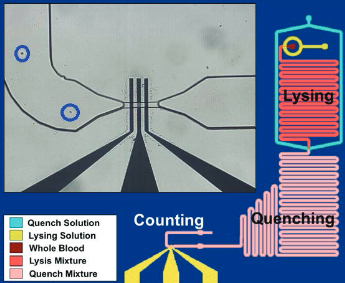
Schematic of the leukocyte counting chip with lysing, quenching, and counter modules shown in different colors. The insert (upper left) is an enlarged view of the platinum microfabricated electrodes (yellow). (credit: U. Hassan et al./TECHNOLOGY)

A microfluidic biosensor that can count red blood cells, platelets, and white blood cells electrically using just one drop of blood (11 microL) has been developed by University of Illinois at Urbana-Champaign (UIUC) researchers, replacing the standard hematology analyzer, a large, expensive lab device that requires trained technicians and physical sample transportation.

The new biosensor can electrically count the different types of blood cells based on their size and membrane properties. To count leukocyte and its differentials, red blood cells are selectively lysed and the remaining white blood cells were individually counted. Specific cells like neutrophils are counted using multi-frequency analysis, which probe the membrane properties of the cells.

The device, which will use credit-card-size disposable cartridges, requires minimal or no experience.  It is expected to find uses in hospitals at the bedside, private clinics, retail clinics, and the developing world.

Patients can perform the test at home in under 20 minutes and share the results with their primary care physicians electronically, reducing the cost of the test to less than $10, compared to $100 or more currently, says UIUc Professor Rashid Bashir, principal investigator.


The research appears in the December 2015 issue of the journal TECHNOLOGY


Abstract of A microfluidic biochip for complete blood cell counts at the point-of-care

Complete blood cell counts (CBCs) are one of the most commonly ordered and informative blood tests in hospitals. The results from a CBC, which typically include white blood cell (WBC) counts with differentials, red blood cell (RBC) counts, platelet counts and hemoglobin measurements, can have implications for the diagnosis and screening of hundreds of diseases and treatments. Bulky and expensive hematology analyzers are currently used as a gold standard for acquiring CBCs. For nearly all CBCs performed today, the patient must travel to either a hospital with a large laboratory or to a centralized lab testing facility. There is a tremendous need for an automated, portable point-of-care blood cell counter that could yield results in a matter of minutes from a drop of blood without any trained professionals to operate the instrument. We have developed microfluidic biochips capable of a partial CBC using only a drop of whole blood. Total leukocyte and their 3-part differential count are obtained from 10 μL of blood after on-chip lysing of the RBCs and counting of the leukocytes electrically using microfabricated platinum electrodes. For RBCs and platelets, 1 μL of whole blood is diluted with PBS on-chip and the cells are counted electrically. The total time for measurement is under 20 minutes. We demonstrate a high correlation of blood cell counts compared to results acquired with a commercial hematology analyzer. This technology could potentially have tremendous applications in hospitals at the bedside, private clinics, retail clinics and the developing world.

AI ‘alarmists’ nominated for 2015 ‘Luddite Award’

An 1844 engraving showing a post-1820s Jacquard loom (credit: public domain/Penny Magazine)

The Information Technology and Innovation Foundation (ITIF) today (Dec. 21) announced 10 nominees for its 2015 Luddite Award. The annual “honor” recognizes the year’s most egregious example of a government, organization, or individual stymieing the progress of technological innovation.

ITIF also opened an online poll and invited the public to help decide the “winner.” The result will be announced in late January.

The nominees include (in no specific order):

1. Alarmists, including respected luminaries such as Elon Musk, Stephen Hawking, and Bill Gates, touting an artificial- intelligence apocalypse.

2. Advocates, including Hawking and Noam Chomsky, seeking a ban on “killer robots.”

3. Vermont and other states limiting automatic license plate readers.

4. Europe, China, and others choosing taxi drivers over car-sharing passengers.

5. The U.S. paper industry opposing e-labeling.

6. California’s governor vetoing RFID tags in driver’s licenses.

7. Wyoming effectively outlawing citizen science.

8. The Federal Communications Commission limiting broadband innovation.

9. The Center for Food Safety fighting genetically improved food.

10. Ohio and other states banning red light cameras.

‘Paranoia about evil machines’

(credit: Paramount Pictures)

“Just as Ned Ludd wanted to smash mechanized looms and halt industrial progress in the 19th century, today’s neo-Luddites want to foil technological innovation to the detriment of the rest of society,” said Robert D. Atkinson, ITIF’s founder and president.

“If we want a world in which innovation thrives, then everyone’s New Year’s resolution should be to replace neo-Luddism with an attitude of risk-taking and faith in the future.”

Atkinson notes that “paranoia about evil machines has swirled around in popular culture for more than 200 years, and these claims continue to grip the popular imagination, in no small part because these apocalyptic ideas are widely represented in books, movies, and music.

“The last year alone saw blockbuster films with a parade of digital villains, such as Avengers: Age of Ultron, Ex Machina, and Terminator: Genisys.”

He also cites statements in Oxford professor Nick Bostrom’s book Superintelligence: Paths, Dangers, Strategies, “reflecting the general fear that ‘superintelligence’ in machines could outperform ‘the best human minds in every field, including scientific creativity, general wisdom and social skills.’ Bostrom argues that artificial intelligence will advance to a point where its goals are no longer compatible with that of humans and, as a result, superintelligent machines will seek to enslave or exterminate us.”

“Raising such sci-fi doomsday scenarios just makes it harder for the public, policymakers,  and scientists to support more funding for AI research, Atkinson concludes. “Indeed, continuing the negative campaign against artificial intelligence could potentially dry up funding for AI research, other than money for how to control, rather than enable AI. What legislator wants to be known as ‘the godfather of the technology that destroyed the human race’?”

Not mentioned in the ITIF statement is the recently announced non-profit “OpenAI” research company founded by Elon Musk and associates, committing $1 billion toward their goal to advance digital intelligence in the way that is most likely to benefit humanity as a whole.”

The 2014 Luddite Award winners

The winners last year: the states of Arizona, Michigan, New Jersey, and Texas, for taking action to prevent Tesla from opening stores in their states to sell cars directly to consumers. Other nominees included:

  • National Rifle Association (NRA) for its opposition to smart guns
  • “Stop Smart Meters” Seeks To Stop Smart Innovation in Meters and Cars
  • Free Press Lobbies for Rules to Stop Innovation in Broadband Networks
  • The Media and Pundits Claiming That “Robots” Are Killing Jobs.


Mystery material stuns scientists

How does water on the surface of this bizarre material control UV light emission and also its conductivity? (credit: Mohammad A. Islam et al./Nano Letters)

In a remarkable chance landmark discovery, a team of researchers at four universities has discovered a mysterious material that emits ultraviolet light and has insulating, electrical conducting, semiconducting, superconducting, and ferromagnetic properties — all controlled by surface water.

It happened while the researchers were studying a sample of lanthanum aluminate film on a strontinum titanate crystal. The sample mysteriously began to glow, emitting intense levels of ultraviolet light from its interior. After carefully reproducing the experimental conditions, they tracked down the unlikely switch that turns UV light on or off: surface water moisture.

The team of researchers from Drexel University, the University of Pennsylvania, the University of California at Berkeley, and Temple University also found that the interface between the materials’ two layers of electrical insulators also had an unusual electrical conducting state that, like UV, could also be altered by the water on the surface. On top of that, the material also exhibited superconducting, ferromagnetic ordering, and photoconductive properties.

Even weirder, “we can also make [the effects] stronger by increasing the distance between the molecules and surface and the buried interface, by using thicker films for example,” said Drexel College of Engineering Professor Jonathan E. Spanier.

Calling in the theorists

Puzzled, the researchers turned to their theory collaborators on the team: Penn’s Andrew M. Rappe, Fenggong Wang, and Diomedes Saldana-Grego.

“Dissociation of water fragments on the oxide surface releases electrons that move to the buried interface, cancelling out the ionic charges,” Wang said. “This puts all the light emission at the same energy, giving the observed sharp photoluminescence.”

According to Rappe, this is the first report of the introduction of molecules to the surface controlling the emission of light — of any color — from a buried solid-surface interface. “The mechanism of a molecule landing and reacting, called dissociative chemisorption, as a way of controlling the onset and suppression of light is unlike any other previously reported,” Saldana-Grego added.

The team recently published its findings in the American Chemical Society journal Nano Letters.

Multiple personality

“We suspect that the material could be used for simple devices like transistors and [chemical] sensors,” said Mohammad Islam, an assistant professor from the State University of New York at Oswego, who was on Spanier’s team when he was at Drexel.

“By strategically placing molecules on the surface, the UV light could be used to relay information — much the way computer memory uses a magnetic field to write and rewrite itself, but with the significant advantage of doing it without an electric current. The strength of the UV field also varies with the proximity of the water molecule; this suggests that the material could also be useful for detecting the presence of chemical agents.”


Abstract of Surface Chemically Switchable Ultraviolet Luminescence from Interfacial Two-Dimensional Electron Gas

We report intense, narrow line-width, surface chemisorption-activated and reversible ultraviolet (UV) photoluminescence from radiative recombination of the two-dimensional electron gas (2DEG) with photoexcited holes at LaAlO3/SrTiO3. The switchable luminescence arises from an electron transfer-driven modification of the electronic structure via H-chemisorption onto the AlO2-terminated surface of LaAlO3, at least 2 nm away from the interface. The control of the onset of emission and its intensity are functionalities that go beyond the luminescence of compound semiconductor quantum wells. Connections between reversible chemisorption, fast electron transfer, and quantum-well luminescence suggest a new model for surface chemically reconfigurable solid-state UV optoelectronics and molecular sensing.

When wearable electronics devices disappear into clothes

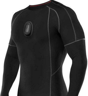
The Athos Upper Body Package includes 14 built in sensors for real-time muscle and heart rate data. (credit: Athos)

Wearables will “disappear” in 2016, predicts New Enterprise Associates venture capital partner Rick Yang, cited in a Wednesday (Dec. 16) CNBC article — integrated “very directly into your everyday life, into your existing fashion sense to the extent that nobody knows you’re wearing a wearable,” he said.

For example, Athos makes smart workout clothes embedded with inconspicuous technology that tracks muscle groups, heart, and breathing rates, he noted.

But taking that next step in wearable technology means ditching bulky, clothes-deforming batteries. Supercapacitors (see “Flexible 3D graphene supercapacitors may power portables and wearables“), as discussed on KurzweilAI, are a perfect match for that. They work like tiny batteries, but unlike batteries, they can be rapidly charged and deliver more power quickly in a smaller space.

They’re a lot smaller and thinner than batteries. But still too bulky.

Weaving electronics into fabrics

Enter Case Western Reserve University researchers, who announced Wednesday that have developed flexible wire-shaped microsupercapacitors that can be embedded as microscopic-sized wires directly in fabrics. These provide three times higher capacitance than previous attempts to create microsupercapacitors, the researchers say.*

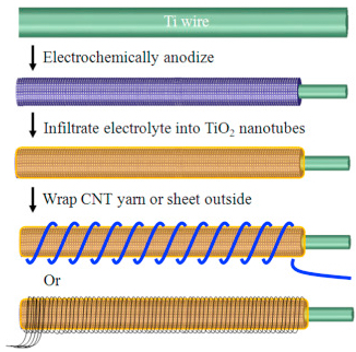
Wearable wires (credit: Tao Chen, Liming Dai/Energy Storage Materials)

In this new design, the modified titanium wire is coated with a solid electrolyte made of polyvinyl alcohol and phosphoric acid. The wire is then wrapped with either yarn or a sheet made of aligned carbon nanotubes, which serves as the second electrode.

The titanium oxide nanotubes, which are semiconducting, separate the two active portions of the electrodes, preventing a short circuit.

“They’re very flexible, so they can be integrated into fabric or textile materials,” said Liming Dai, the Kent Hale Smith Professor of Macromolecular Science and Engineering. “They can be a wearable, flexible power source for wearable electronics and also for self-powered biosensors or other biomedical devices, particularly for applications inside the body.”

The scientists published their research on the microsupercapacitor in the journal Energy Storage Materials this week. The study builds on earlier carbon-based supercapacitors.

Conductive inks

An article just published in Chemical & Engineering News (C&EN) profiles textiles printed with such stretchable embedded wiring and electronic sensors, which can transmit data wirelessly and withstand washing.

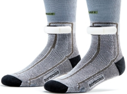
Smart socks (credit: Sensoria)

For example, “smart socks” incorporate stretchable silver-based conductive yarns that connect their sensors to a magnetic Bluetooth electronic anklet that transmits data to a mobile app to keep track of foot landings, cadence, and time on the ground.

The data are intended to help runners improve their form and performance. Two pairs of socks and an anklet cost $200.

C&EN also highlights another key technology: conductive inks, which are used by BeBop Sensors in a design for a thin shoe insole integrated with piezoresistive-fabric sensors and silicon-based electronics, which are capable of measuring a wearer’s foot pressure.

They’ve also developed a conceptual design for a car steering wheel cover that senses driver alertness and weight-lifting gloves that sense weight and load distribution between hands.

Mounir Zok, senior sports technologist for the U.S. Olympic Committee dates the beginning of wearable technology to 2002, when relatively small electronic devices first began to replace the probes, electrodes, and masks that athletes wore while tethered to monitoring equipment in training labs, C&EN notes.

Devices to measure heart rate, power, cadence, and speed can lead to improved performance for athletes, Zok explained. Many of the first wearable devices designed for track and field were cumbersome and interfered with performance. But the smaller, more flexible, less power-hungry devices available today are helping Zok and his colleagues better monitor athletic improvements.

* In a lab experiment, the microsupercapactitor was able to store 1.84 milliFarads per micrometer. Energy density was 0.16 x 10⁻³ milliwatt-hours per cubic centimeter and power density .01 milliwatt per cubic centimeter.


Abstract of Flexible and wearable wire-shaped microsupercapacitors based on highly aligned titania and carbon nanotubes

Wire-shaped devices, such as solar cells and supercapacitors, have attracted great attentions due to their unique structure and promise to be integrated into textiles as portable energy source. To date, most reported wire-shaped supercapacitors were developed based on carbon nanomaterial-derived fiber electrodes whereas titania was much less used, though with excellent pseudocapacitvie properties. In this work, we used a titanium wire sheathed with radially aligned titania nanotubes as one of the electrodes to construct all-solid-state microsupercapacitors, in which the second electrode was carbon nanotube fiber or sheet. The capacitance of the resulting microsupercapacitor with a CNT sheet electrode (1.84 mF cm−2) is about three time of that for the corresponding device with the second electrode based on a single CNT yarn. The unique wire-shaped structure makes it possible for the wire-shaped microsupercapacitors to be woven into various textiles and connected in series or parallel to meet a large variety of specific energy demands.