New microscope creates near-real-time videos of nanoscale processes


MIT | Microscope creates near-real-time videos of nanoscale processes

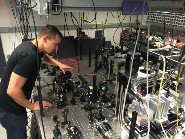
MIT engineers have designed an atomic force microscope (AFM) that scans images 2,000 times faster than existing commercial models. Operating at near-real-time-video speed, it can capture structures as small as a fraction of a nanometer from single strands of DNA down to individual hydrogen bonds.

Existing AFMs have similar spatial resolution but function at slow speeds.

In one dramatic demonstration of the instrument’s capabilities (see video), the researchers scanned a 70- by-70-micrometers sample of calcite as it was first immersed in deionized water and later exposed to sulfuric acid. Over a period of several seconds, the team observed the acid eating away at the calcite, expanding existing nanometer-sized pits in the material that quickly merged and led to a layer-by-layer removal of calcite along the material’s crystal pattern.
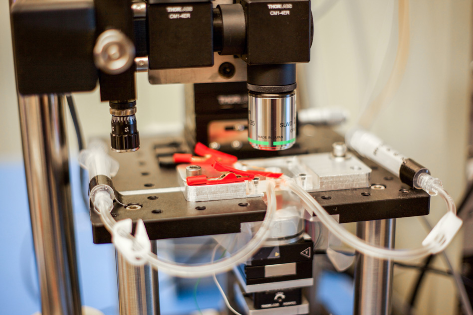
The new MIT high-speed microscope produces images of chemical processes taking place at the nanoscale at a rate that is close to real-time video. This closeup shot of the microscope shows transparent tubes used to inject various liquids into the imaging environment. This liquid can be water, acid, buffer solution for live bacteria, cells, or electrolytes in an electrochemical process. Researchers use one as an inlet and the other as an outlet to circulate and refresh the solutions throughout the experiment. (credit: Jose-Luis Olivares/MIT)

Kamal Youcef-Toumi, a professor of mechanical engineering at MIT, says the instrument’s sensitivity and speed will enable scientists to watch atomic-sized processes play out as high-resolution “movies” for the first time.

“People can see, for example, condensation, nucleation, dissolution, or deposition of material, and how these happen in real-time — things that people have never seen before,” Youcef-Toumi says. “This is fantastic to see these details emerging. And it will open great opportunities to explore all of this world that is at the nanoscale.”
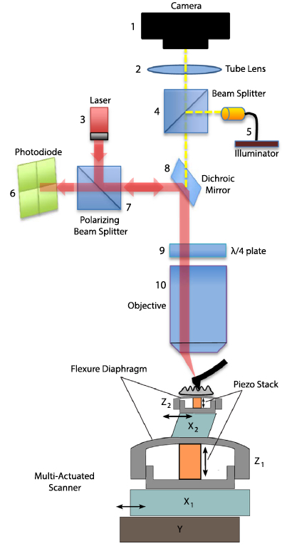
A schematic of the AFM (credit: I. Soltani Bozchalooi et al./Ultramicroscopy)

The group’s design and images, which are based on the PhD work of Iman Soltani Bozchalooi, now a postdoc in the Department of Mechanical Engineering, are published in the journal Ultramicroscopy.

Atomic force microscopes typically scan samples using an ultrafine probe, or needle, that skims along the surface of a sample, tracing its topography, similarly to how a blind person reads Braille. Samples sit on a movable platform, or scanner, that moves the sample laterally and vertically beneath the probe.

Because AFMs scan incredibly small structures, the instruments have to work slowly, line by line, to avoid any sudden movements that could alter the sample or blur the image. Such conventional microscopes typically scan only about one to two lines per second.

To speed up the scanning process, scientists have built platforms that scan samples more quickly, but over a smaller area, and the platforms don’t allow scientists to zoom out to see a wider view or study larger features.

Synchronized Scanners

The main innovation of the new design is a multi-actuated scanner. The sample platform incorporates both a smaller, speedier scanner and a larger, slower scanner for every direction, which work together as one system to scan a wide 3-D region at high speed.

The microscope operates at about eight to 10 frames per second and can scan across hundreds of microns and image features that are several microns high.

“We want to go to real video, which is at least 30 frames per second,” Youcef-Toumi says. “Hopefully we can work on improving the instrument and controls so that we can do video-rate imaging while maintaining its large range and keeping it user-friendly.”


Abstract of Design and control of multi-actuated atomic force microscope for large-range and high-speed imaging
This paper presents the design and control of a high-speed and large-range atomic force microscopy (AFM). A multi-actuation scheme is proposed where several nano-positioners cooperate to achieve the range and speed requirements. A simple data-based control design methodology is presented to effectively operate the AFM scanner components. The proposed controllers compensate for the coupled dynamics and divide the positioning responsibilities between the scanner components. As a result, the multi-actuated scanner behavior is equivalent to that of a single XYZ positioner with large range and high speed. The scanner of the designed AFM is composed of five nano-positioners, features 6 μm out-of-plane and 120 μm lateral ranges and is capable of high-speed operation. The presented AFM has a modular design with laser spot size of 3.5 μm suitable for small cantilever, an optical view of the sample and probe, a conveniently large waterproof sample stage and a 20 MHz data throughput for high resolution image acquisition at high imaging speeds. This AFM is used to visualize etching of calcite in a solution of sulfuric acid. Layer-by-layer dissolution and pit formation along the crystalline lines in a low pH environment is observed in real time.


Abstract of Multi-actuation and PI control: A simple recipe for high-speed and large-range atomic force microscopy

High speed atomic force microscopy enables observation of dynamic nano-scale processes. However, maintaining a minimal interaction force between the sample and the probe is challenging at high speed specially when using conventional piezo-tubes. While rigid AFM scanners are operational at high speeds with the drawback of reduced tracking range, multi-actuation schemes have shown potential for high-speed and large-range imaging. Here we present a method to seamlessly incorporate additional actuators into conventional AFMs. The equivalent behavior of the resulting multi-actuated setup resembles that of a single high-speed and large-range actuator with maximally flat frequency response. To achieve this, the dynamics of the individual actuators and their couplings are treated through a simple control scheme. Upon the implementation of the proposed technique, commonly used PI controllers are able to meet the requirements of high-speed imaging. This forms an ideal platform for retroactive enhancement of existing AFMs with minimal cost and without compromise on the tracking range. A conventional AFM with tube scanner is retroactively enhanced through the proposed method and shows an order of magnitude improvement in closed loop bandwidth performance while maintaining large range. The effectiveness of the method is demonstrated on various types of samples imaged in contact and tapping modes, in air and in liquid.

New transparent metal films may radically reduce costs for smartphone, tablet and TV displays

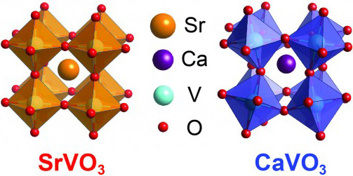
A figure showing the crystal structure of strontium vanadate (orange) and calcium vanadate (blue). The red dots are oxygen atoms arranged in 8 octohedra surrounding a single strontium or calcium atom. Vanadium atoms can be seen inside each octahedron. (credit: Lei Zhang/Penn State)

A new material that is both highly transparent and electrically conductive could make large screen displays, smart windows, touch screens, and solar cells more affordable and efficient, according to materials scientists and engineers at Penn State who have discovered just such a material.

Indium tin oxide (ITO), the transparent conductor that is now used for more than 90 percent of the display market, has been the dominant material for the past 60 years. But in the last decade, the price of indium has increased dramatically. Displays and touchscreen modules have become a main cost driver in mobile devices, such as smartphones and tablets, making up close to 40 percent of the cost.

As as result, while memory chips and processors get cheaper, smartphone and tablet displays get more expensive from generation to generation. Manufacturers have searched for a possible ITO replacement, but until now, nothing has matched ITO’s combination of optical transparency, electrical conductivity, and ease of fabrication.

New display materials

In a paper appearing Tuesday (Dec 15) online in Nature Materials, Roman Engel-Herbert, assistant professor of materials science and engineering, and his team report a new design strategy that approaches the problem from a different angle.

The researchers use thin (10 nanometer) films of an unusual class of materials called correlated metals in which the electrons flow like a liquid. In most conventional metals, such as copper, gold, aluminum or silver, electrons flow like a gas; in correlated metals, such as strontium vanadate and calcium vanadate, they move like a liquid. These correlated metals show a high optical transparency despite their high, metal-like conductivity.

“We are trying to make metals transparent by changing the effective mass of their electrons,” Engel-Herbert says. “We are doing this by choosing materials in which the electrostatic interaction between negatively charged electrons is very large compared to their kinetic energy. As a result of this strong electron correlation effect, electrons ‘feel’ each other and behave like a liquid rather than a gas of non-interacting particles. This electron liquid is still highly conductive, but when you shine light on it, it becomes less reflective, thus much more transparent.”

Less than 5 percent of the cost of current display materials

Currently, indium costs around $750 per kilogram, whereas strontium vanadate and calcium vanadate are made from elements with orders of magnitude higher abundance in the earth’s crust. Vanadium sells for around $25 a kilogram, less than 5 percent of the cost of indium, while strontium is even cheaper than vanadium.

“Our correlated metals work really well compared to ITO. Now, the question is how to implement these new materials in a large scale manufacturing process. From what we understand right now, there is no reason that strontium vanadate could not replace ITO in the same equipment currently used in industry,” says Engel-Herbert.

Along with display technologies, Engel-Herbert and his group plan to combine their new materials with a promising type of solar cell that uses a class of materials called organic perovskites. Developed only within the last half dozen years, these materials outperform commercial silicon solar cells but still require an inexpensive transparent conductor. Strontium vanadate, also a perovskite, has a compatible structure that makes this an interesting possibility for future inexpensive, high-efficiency solar cells.

The Office of Naval Research, the National Science Foundation, and the Department of Energy funded this work.


Abstract of Correlated metals as transparent conductors

The fundamental challenge for designing transparent conductors used in photovoltaics, displays and solid-state lighting is the ideal combination of high optical transparency and high electrical conductivity. Satisfying these competing demands is commonly achieved by increasing carrier concentration in a wide-bandgap semiconductor with low effective carrier mass through heavy doping, as in the case of tin-doped indium oxide (ITO). Here, an alternative design strategy for identifying high-conductivity, high-transparency metals is proposed, which relies on strong electron–electron interactions resulting in an enhancement in the carrier effective mass. This approach is experimentally verified using the correlated metals SrVO3 and CaVO3, which, despite their high carrier concentration (>2.2 × 1022 cm−3), have low screened plasma energies (<1.33 eV), and demonstrate excellent performance when benchmarked against ITO. A method is outlined to rapidly identify other candidates among correlated metals, and strategies are proposed to further enhance their performance, thereby opening up new avenues to develop transparent conductors.

Will this DNA molecular switch replace conventional transistors?

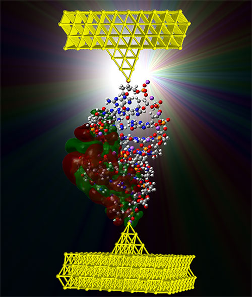
A model of one form of double-stranded DNA attached to two electrodes (credit: UC Davis)

What do you call a DNA molecule that changes between high and low electrical conductance (amount of current flow)?

Answer: a molecular switch (transistor) for nanoscale computing. That’s what a team of researchers from the University of California, Davis and the University of Washington have documented in a paper published in Nature Communications Dec. 9.

“As electronics get smaller they are becoming more difficult and expensive to manufacture, but DNA-based devices could be designed from the bottom-up using directed self-assembly techniques such as ‘DNA origami’,” said Josh Hihath, assistant professor of electrical and computer engineering at UC Davis and senior author on the paper.

DNA origami is the folding of DNA to create two- and three-dimensional shapes at the nanoscale level (see DNA origami articles on KurzweilAI).

Hihath suggests that DNA-based devices may also improve the energy efficiency of electronic circuits, compared to traditional transistors, where power density on-chip has increased as transistors have become miniaturized, limiting further miniaturization.

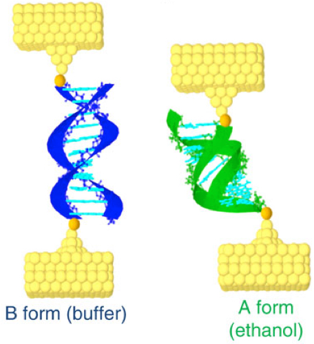
This illustration shows double-stranded DNA in two configurations, B-form (blue) and A-form (green), bound to gold electrodes (yellow). The linkers to the electrodes (either amines or thiols) are shown in orange. (credit: Juan Manuel Artés et al./Nature Communications)

To develop DNA into a reversible switch, the scientists focused on switching between two stable conformations of DNA, known as the A-form and the B-form. In DNA, the B-form is the conventional DNA duplex molecule. The A-form is a more compact version with different spacing and tilting between the base pairs. Exposure to ethanol forces the DNA into the A-form conformation, resulting in increased conductance. Removing the ethanol causes the DNA to switch back to the B-form and return to its original reduced conductance value.

But the authors advise that to develop this finding into a technologically viable platform for electronics will require a great deal of work to overcome two major hurdles: billions of active DNA molecular devices must be integrated into the same circuit, as is done currently in conventional electronics; and scientists must be able to gate specific devices individually in such a large system.


Abstract of Conformational gating of DNA conductance

DNA is a promising molecule for applications in molecular electronics because of its unique electronic and self-assembly properties. Here we report that the conductance of DNA duplexes increases by approximately one order of magnitude when its conformation is changed from the B-form to the A-form. This large conductance increase is fully reversible, and by controlling the chemical environment, the conductance can be repeatedly switched between the two values. The conductance of the two conformations displays weak length dependencies, as is expected for guanine-rich sequences, and can be fit with a coherence-corrected hopping model. These results are supported by ab initio electronic structure calculations that indicate that the highest occupied molecular orbital is more disperse in the A-form DNA case. These results demonstrate that DNA can behave as a promising molecular switch for molecular electronics applications and also provide additional insights into the huge dispersion of DNA conductance values found in the literature.

Skyscraper-style carbon-nanotube chip design ‘boosts electronic performance by factor of a thousand’

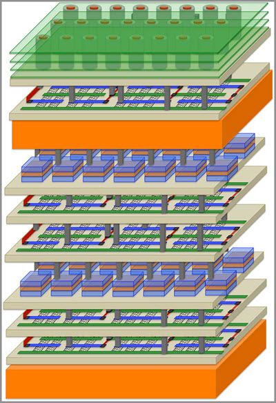
A new revolutionary high-rise architecture for computing (credit: Stanford University)

Researchers at Stanford and three other universities are creating a revolutionary new skyscraper-like high-rise architecture for computing based on carbon nanotube materials instead of silicon.

In Rebooting Computing, a special issue (in press) of the IEEE Computer journal, the team describes its new approach as “Nano-Engineered Computing Systems Technology,” or N3XT.

Suburban-style chip layouts create long commutes and regular traffic jams in electronic circuits, wasting time and energy, they note.

N3XT will break data bottlenecks by integrating processors and memory-like floors in a skyscraper and by connecting these components with millions of “vias,” which play the role of tiny electronic elevators.

The N3XT high-rise approach will move more data, much faster, using far less energy, than would be possible using low-rise circuits, according to the researchers.

Stanford researchers including Associate Professor Subhasish Mitra and Professor H.-S. Philip Wong have “assembled a group of top thinkers and advanced technologies to create a platform that can meet the computing demands of the future,” Mitra says.

“When you combine higher speed with lower energy use, N3XT systems outperform conventional approaches by a factor of a thousand,” Wong claims.

Carbon nanotube transistors

Engineers have previously tried to stack silicon chips but with limited success, the researchers suggest. Fabricating a silicon chip requires temperatures close to 1,800 degrees Fahrenheit, making it extremely challenging to build a silicon chip atop another without damaging the first layer. The current approach to what are called 3-D, or stacked, chips is to construct two silicon chips separately, then stack them and connect them with a few thousand wires.

But conventional 3-D silicon chips are still prone to traffic jams and it takes a lot of energy to push data through what are a relatively few connecting wires.

The N3XT team is taking a radically different approach: building layers of processors and memory directly atop one another, connected by millions of vias that can move more data over shorter distances that traditional wire, using less energy, and immersing computation and memory storage into an electronic super-device.

The key is the use of non-silicon materials that can be fabricated at much lower temperatures than silicon, so that processors can be built on top of memory without the new layer damaging the layer below. As in IBM’s recent chip breakthrough (see “Method to replace silicon with carbon nanotubes developed by IBM Research“), N3XT chips are based on carbon nanotube transistors.

Transistors are fundamental units of a computer processor, the tiny on-off switches that create digital zeroes and ones. CNTs are faster and more energy-efficient than silicon processors, and much thinner. Moreover, in the N3XT architecture, they can be fabricated and placed over and below other layers of memory.

Among the N3XT scholars working at this nexus of computation and memory are Christos Kozyrakis and Eric Pop of Stanford, Jeffrey Bokor and Jan Rabaey of the University of California, Berkeley, Igor Markov of the University of Michigan, and Franz Franchetti and Larry Pileggi of Carnegie Mellon University.

New storage technologies 

Team members also envision using data storage technologies that rely on materials other than silicon. This would allow for the new materials to be manufactured on top of CNTs, using low-temperature fabrication processes.

One such data storage technology is called resistive random-access memory, or RRAM (see “‘Memristors’ based on transparent electronics offer technology of the future“). Resistance slows down electrons, creating a zero, while conductivity allows electrons to flow, creating a one. Tiny jolts of electricity switch RRAM memory cells between these two digital states. N3XT team members are also experimenting with a variety of nanoscale magnetic storage materials.

Just as skyscrapers have ventilation systems, N3XT high-rise chip designs incorporate thermal cooling layers. This work, led by Stanford mechanical engineers Kenneth Goodson and Mehdi Asheghi, ensures that the heat rising from the stacked layers of electronics does not degrade overall system performance.

Mitra and Wong have already demonstrated a working prototype of a high-rise chip. At the International Electron Devices Meeting in December 2014 they unveiled a four-layered chip made up of two layers of RRAM memory sandwiched between two layers of CNTs (see “Stanford engineers invent radical ‘high-rise’ 3D chips“).

In their N3XT paper they ran simulations showing how their high-rise approach was a thousand times more efficient in carrying out many important and highly demanding industrial software applications.


AI will replace smartphones within 5 years, Ericsson survey suggests

(credit: Ericsson ConsumerLab)

Artificial intelligence (AI) interfaces will take over, replacing smartphones in five years, according to a survey of more than 5000 smartphone customers in nine countries by Ericsson ConsumerLab in the fifth edition of its annual trend report, 10 Hot Consumer Trends 2016 (and beyond).

Smartphone users believe AI will take over many common activities, such as searching the net, getting travel guidance, and as personal assistants. The survey found that 44 percent think an AI system would be as good as a teacher and one third would like an AI interface to keep them company. A third would rather trust the fidelity of an AI interface than a human for sensitive matters; and 29 percent agree they would feel more comfortable discussing their medical condition with an AI system.

However, many of the users surveyed find smartphones limited.

Impractical. Constantly having a screen in the palm of your hand is not always a practical solution, such as in driving or cooking.

Battery capacity limits. One in 3 smartphone users want a 7−8 inch screen, creating a battery drain vs. size and weight issue.

Not wearable. 85 percent of the smartphone users think intelligent wearable electronic assistants will be commonplace within 5 years, reducing the need to always touch a screen. And one in two users believes they will be able to talk directly to household appliances.

VR and 3D better. The smartphone users want movies that play virtually around the viewer, virtual tech support, and VR headsets for sports, and more than 50 percent of consumers think holographic screens will be mainstream within 5 years — capabilities not available in a small handheld device. Half of the smartphone users want a 3D avatar to try on clothes online, and 64 percent would like the ability to see an item’s actual size and form when shopping online. Half of the users want to bypass shopping altogether, with a 3D printer for printing household objects such as spoons, toys and spare parts for appliances; 44 percent even want to print their own food or nutritional supplements.

The 10 hot trends for 2016 and beyond cited in the report

  1. The Lifestyle Network Effect. Four out of five people now experience an effect where the benefits gained from online services increases as more people use them. Globally, one in three consumers already participates in various forms of the sharing economy.
  2. Streaming NativesTeenagers watch more YouTube video content daily than other age groups. Forty-six percent of 16-19 year-olds spend an hour or more on YouTube every day.
  3. AI Ends The Screen AgeArtificial intelligence will enable interaction with objects without the need for a smartphone screen. One in two smartphone users think smartphones will be a thing of the past within the next five years.
  4. Virtual Gets RealConsumers want virtual technology for everyday activities such as watching sports and making video calls. Forty-four percent even want to print their own food.
  5. Sensing Homes. Fifty-five percent of smartphone owners believe bricks used to build homes could include sensors that monitor mold, leakage and electricity issues within the next five years. As a result, the concept of smart homes may need to be rethought from the ground up.
  6. Smart CommutersCommuters want to use their time meaningfully and not feel like passive objects in transit. Eighty-six percent would use personalized commuting services if they were available.
  7. Emergency ChatSocial networks may become the preferred way to contact emergency services. Six out of 10 consumers are also interested in a disaster information app.
  8. InternablesInternal sensors that measure well-being in our bodies may become the new wearables. Eight out of 10 consumers would like to use technology to enhance sensory perceptions and cognitive abilities such as vision, memory and hearing.
  9. Everything Gets HackedMost smartphone users believe hacking and viruses will continue to be an issue. As a positive side-effect, one in five say they have greater trust in an organization that was hacked but then solved the problem.
  10. Netizen JournalistsConsumers share more information than ever and believe it increases their influence on society. More than a third believe blowing the whistle on a corrupt company online has greater impact than going to the police.

Source: 10 Hot Consumer Trends 2016. Ericsson ConsumerLab, Information Sharing, 2015. Base: 5,025 iOS/Android smartphone users aged 15-69 in Berlin, Chicago, Johannesburg, London, Mexico City, Moscow, New York, São Paulo, Sydney and Tokyo

Hybrid solid-state chips and biological cells integrated at molecular level

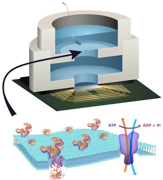
Illustration depicting a biocell attached to a CMOS integrated circuit with a membrane containing sodium-potassium pumps in pores. Energy is stored chemically in ATP molecules. When the energy is released as charged ions (which are then converted to electrons to power the chip at the bottom of the experimental device), the ATP is converted to ADP + inorganic phosphate. (credit: Trevor Finney and Jared Roseman/Columbia Engineering)

Columbia Engineering researchers have combined biological and solid-state components for the first time, opening the door to creating entirely new artificial biosystems.

In this experiment, they used a biological cell to power a conventional solid-state complementary metal-oxide-semiconductor (CMOS) integrated circuit. An artificial lipid bilayer membrane containing adenosine triphosphate (ATP)-powered ion pumps (which provide energy for cells) was used as a source of ions (which were converted to electrons to power the chip).

The study, led by Ken Shepard, Lau Family Professor of Electrical Engineering and professor of biomedical engineering at Columbia Engineering, was published online today (Dec. 7, 2015) in an open-access paper in Nature Communications.

How to build a hybrid biochip

Living systems achieve this functionality with their own version of electronics based on lipid membranes and ion channels and pumps, which act as a kind of “biological transistor.” Charge in the form of ions carry energy and information, and ion channels control the flow of ions across cell membranes.

Solid-state systems, such as those in computers and communication devices, use electrons; their electronic signaling and power are controlled by field-effect transistors.

To build a prototype of their hybrid system, Shepard’s team packaged a CMOS integrated circuit (IC) with an ATP-harvesting “biocell.” In the presence of ATP, the system pumped ions across the membrane, producing an electrical potential (voltage)* that was harvested by the integrated circuit.

“We made a macroscale version of this system, at the scale of several millimeters, to see if it worked,” Shepard notes. “Our results provide new insight into a generalized circuit model, enabling us to determine the conditions to maximize the efficiency of harnessing chemical energy through the action of these ion pumps. We will now be looking at how to scale the system down.”

While other groups have harvested energy from living systems, Shepard and his team are exploring how to do this at the molecular level, isolating just the desired function and interfacing this with electronics. “We don’t need the whole cell,” he explains. “We just grab the component of the cell that’s doing what we want. For this project, we isolated the ATPases because they were the proteins that allowed us to extract energy from ATP.”

The capability of a bomb-sniffing dog, no Alpo required

Next, the researchers plan to go much further, such as recognizing specific molecules and giving chips the potential to taste and smell.

The ability to build a system that combines the power of solid-state electronics with the capabilities of biological components has great promise, they believe. “You need a bomb-sniffing dog now, but if you can take just the part of the dog that is useful — the molecules that are doing the sensing — we wouldn’t need the whole animal,” says Shepard.

The technology could also provide a power source for implanted electronic devices in ATP-rich environments such as inside living cells, the researchers suggest.

*  “In general, integrated circuits, even when operated at the point of minimum energy in subthreshold, consume on the order of 10−2 W mm−2 (or assuming a typical silicon chip thickness of 250 μm, 4 × 10⁻² W mm−3). Typical cells, in contrast, consume on the order of 4 × 10⁻⁶ W mm−3. In the experiment, a typical active power dissipation for the IC circuit was 92.3 nW, and the active average harvesting power was 71.4 fW for the biocell (the discrepancy is managed through duty-cycled operation of the IC).” — Jared M. Roseman et al./Nature Communications


White graphene + graphene –> super-thin, cooler, more flexible electronics

Growth and transfer of 2-D material such as hexagonal boron nitride and graphene was performed by a team that included Yijing Stehle of Oak Ridge National Laboratory. (credit: ORNL)

A new era of electronics and even quantum devices could be ushered in with the fabrication of a virtually perfect single layer of “white graphene,” according to researchers at the Department of Energy’s Oak Ridge National Laboratory.

The material is technically known as hexagonal boron nitride (see “New inventions track greenhouse gas, remediate oil spills“). It is an insulator (instead of a conductor of electricity as with graphene), so it could serve as a 2-D dielectric (insulating material) in electronic devices such as thin-film capacitors.

It also has even better transparency than graphene, making it useful as a substrate and the foundation for the electronics in cell phones, laptops, tablets and many other devices.

“As thin as a piece of paper”

ORNL’s Yijing Stehle, postdoctoral associate and lead author of a paper published in Chemistry of Materials and colleagues are working on combining graphene and boron nitride in a 2-D capacitor and fuel cell prototype that are “super thin” and also transparent.

With their recipe for white graphene, ORNL researchers hope to unleash the full potential of graphene as a conductor. By combining it with white graphene as a substrate, researchers believe they can make thinner, more-flexible multilayer electronic devices.

“Imagine batteries, capacitors, solar cells, video screens and fuel cells as thin as a piece of paper,” she said.

For its part, graphene on a white-graphene substrate also has several thousand times higher electron mobility than using graphene on other substrates. That feature could enable data transfers that are much faster than what is available today.

Cool electronics

A recent theoretical study led by Rice University proposed the use of white graphene to cool electronics (see “Why ‘white graphene’ structures are cool“). Stehle and colleagues have made high-quality layers of hexagonal boron nitride that support that study; they believe the material can be cost-effectively scaled up to large production volumes.

The Rice process consists of standard atmospheric pressure chemical vapor deposition with a similar furnace, temperature and time. But Stehle describes “a more gentle, controllable way to release the reactant into the furnace and figuring out how to take advantage of inner furnace conditions.”

New Mexico State University researchers were also involved in the study, which was supported by the DOE’s Office of Science.


Abstract of Synthesis of Hexagonal Boron Nitride Monolayer: Control of Nucleation and Crystal Morphology

Monolayer hexagonal boron nitride (hBN) attracts significant attention due to the potential to be used as a complementary two-dimensional dielectric in fabrication of functional 2D heterostructures. Here we investigate the growth stages of the hBN single crystals and show that hBN crystals change their shape from triangular to truncated triangular and further to hexagonal depending on copper substrate distance from the precursor. We suggest that the observed hBN crystal shape variation is affected by the ratio of boron to nitrogen active species concentrations on the copper surface inside the CVD reactor. Strong temperature dependence reveals the activation energies for the hBN nucleation process of ∼5 eV and crystal growth of ∼3.5 eV. We also show that the resulting h-BN film morphology is strongly affected by the heating method of borazane precursor and the buffer gas. Elucidation of these details facilitated synthesis of high quality large area monolayer hexagonal boron nitride by atmospheric pressure chemical vapor deposition on copper using borazane as a precursor.

‘Invisible wires’ could improve solar-cell efficiency

Silicon pillars emerge from nanosize holes in a thin gold film. The pillars funnel 97 percent of incoming light to a silicon substrate, a technology that could significantly boost the performance of conventional solar cells. (credit: Vijay Narasimhan, Stanford University)

Stanford scientists have discovered how to make the electrical wiring on top of solar cells nearly invisible to incoming light, using nanosize silicon pillars to hide the wires. The new design could dramatically boost solar-cell efficiency, the researchers suggest.

A solar cell is basically a semiconductor that converts sunlight into electricity, sandwiched between metal contacts that carry the electrical current generated by the cell. But with current designs, the shiny metal wires on top of the cell reflect sunlight away from the semiconductor surface, reducing the cell’s efficiency.

Now Stanford scientists have discovered how to hide the reflective upper contacts, funneling light directly to the semiconductor below by using silicon pillars to redirect the sunlight before it hits the metallic surface.


Stanford University | “Invisible wires” could boost solar-cell efficiency

Besides gold, the nanopillar architecture will  also work with contacts made of silver, platinum, nickel and other metals. In addition to silicon, this new technology can be used with other semiconducting materials for a variety of applications, including photosensors, light-emitting diodes and displays and transparent batteries, as well as solar cells.

The new method aims to improve on a wide variety of methods that have been reported by KurzweilAI.

The findings are published in the journal ACS Nano.


Abstract of Hybrid Metal–Semiconductor Nanostructure for Ultrahigh Optical Absorption and Low Electrical Resistance at Optoelectronic Interfaces

Engineered optoelectronic surfaces must control both the flow of light and the flow of electrons at an interface; however, nanostructures for photon and electron management have typically been studied and optimized separately. In this work, we unify these concepts in a new hybrid metal–semiconductor surface that offers both strong light absorption and high electrical conductivity. We use metal-assisted chemical etching to nanostructure the surface of a silicon wafer, creating an array of silicon nanopillars protruding through holes in a gold film. When coated with a silicon nitride anti-reflection layer, we observe broad-band absorption of up to 97% in this structure, which is remarkable considering that metal covers 60% of the top surface. We use optical simulations to show that Mie-like resonances in the nanopillars funnel light around the metal layer and into the substrate, rendering the metal nearly transparent to the incoming light. Our results show that, across a wide parameter space, hybrid metal–semiconductor surfaces with absorption above 90% and sheet resistance below 20 Ω/□ are realizable, suggesting a new paradigm wherein transparent electrodes and photon management textures are designed and fabricated together to create high-performance optoelectronic interfaces.

Quantum entanglement achieved at room temperature in macroscopic semiconductor wafers

Paul Klimov, a graduate student in the University of Chicago’s Institute for Molecular Engineering, adjusts the intensity of a laser beam during an experiment. (credit: Awschalom Group/University of Chicago)

Researchers in Prof. David Awschalom’s group at the Institute for Molecular Engineering have demonstrated macroscopic entanglement at room temperature and in a small (33 millitesla) magnetic field.

Previously, scientists have overcome the thermodynamic barrier and achieved macroscopic entanglement in solids and liquids by going to ultra-low temperatures (-270 degrees Celsius) and applying huge magnetic fields (1,000 times larger than that of a typical refrigerator magnet) or using chemical reactions.

In an open-access paper published in the Nov. 20 issue of Science Advances, the researchers explain that they used infrared laser light to order (preferentially align) the magnetic states of thousands of electrons and nuclei and then used electromagnetic pulses to entangle them. This procedure caused pairs of electrons and nuclei in a macroscopic 40 micrometer-cubed volume (the volume of a red blood cell) in a silicon carbide (SiC, also known as carborundum) semiconductor wafer to become entangled.

“The ability to produce robust entangled states in an electronic-grade semiconductor at ambient conditions has important implications on future quantum devices,” Awschalom said. In the short term, the research could enable quantum sensors that use entanglement as a resource for beating the sensitivity limit of traditional (non-quantum) sensors and for biological sensing inside a living organism, using entanglement-enhanced magnetic resonance imaging probes, according to the researchers.

They said that it might even be possible in the long term to go from entangled states on the same SiC chip to entangled states across distant SiC chips via macroscopic quantum states, as opposed to single quantum states (in single atoms). Such long-distance entangled states have been proposed for synchronizing global positioning satellites and for communicating information secured from eavesdroppers.

The institute is a partnership of the University of Chicago and and Argonne National Laboratory.


Abstract of Quantum entanglement at ambient conditions in a macroscopic solid-state spin ensemble

Entanglement is a key resource for quantum computers, quantum-communication networks, and high-precision sensors. Macroscopic spin ensembles have been historically important in the development of quantum algorithms for these prospective technologies and remain strong candidates for implementing them today. This strength derives from their long-lived quantum coherence, strong signal, and ability to couple collectively to external degrees of freedom. Nonetheless, preparing ensembles of genuinely entangled spin states has required high magnetic fields and cryogenic temperatures or photochemical reactions. We demonstrate that entanglement can be realized in solid-state spin ensembles at ambient conditions. We use hybrid registers comprising of electron-nuclear spin pairs that are localized at color-center defects in a commercial SiC wafer. We optically initialize 103 identical registers in a 40-μm3 volume (with Embedded Image fidelity) and deterministically prepare them into the maximally entangled Bell states (with 0.88 ± 0.07 fidelity). To verify entanglement, we develop a register-specific quantum-state tomography protocol. The entanglement of a macroscopic solid-state spin ensemble at ambient conditions represents an important step toward practical quantum technology.


New ‘tricorder’ technology might be able to ‘hear’ tumors

Capacitive micromachined ultrasonic detectors used in the experiments, with a detail view of the front and back of one device (credit: Hao Nan et al./Applied Physics Letters)

Stanford electrical engineers have developed an enhancement of technology intended to safely find buried plastic explosives and spot fast-growing tumors, using a combination of microwaves and ultrasound to develop a detector similar to the legendary Star Trek tricorder.

The work, led by Assistant Professor Amin Arbabian and Research Professor Pierre Khuri-Yakub, grows out of DARPA research designed to detect buried plastic explosives, but the researchers said the technology could also provide a new way to detect early stage cancers.

The new work was spurred by a challenge posed by the Defense Advanced Research Projects Agency (DARPA), which sought a system to detect plastic explosives (improvised explosive devices or IEDs) buried underground, which are currently invisible to metal detectors. The detection device could not touch the surface in question, so as not to trigger an explosion.

The engineers developed a system based on the principle that all materials expand and contract when heated, but not at identical rates. In a potential battlefield application, the microwaves would heat the suspect area, causing the muddy ground to absorb energy and expand, and thus squeeze the plastic. Pulsing the microwaves would then generate a series of ultrasound pressure waves that could be detected and interpreted to disclose the presence of buried plastic explosives.

Touchless ultrasound detection

Sound waves propagate differently in solids than air, with a drastic transmission loss occurring when sound jumps from the solid to air. So the Stanford team accommodated for this loss by building highly sensitive capacitive micromachined ultrasonic transducers (CMUTs) that can specifically discern the weaker ultrasound signals that jumped from the solid, through the air, to the detector.

Solving the technical challenges of detecting ultrasound after it left the ground gave the Stanford researchers the experience to take aim at their ultimate goal: Using the device in medical applications without touching the skin.

Schematic of the non-contact thermoacoustic detection setup. H is the thickness of the surrounding packaging material (set to between 1 and 3 cm of water or Agarose), corresponding to the surrounding flesh-like tissue. T is the thickness of the embedded target (Rexolite, in this case, set to 4mm layers and target area of 4 square cm), corresponding to a tumor. In microwave-induced thermoacoustic imaging, the target absorbs a portion of the microwave electromagnetic energy (from the microwave signal generator) based on the the target tissue’s dielectric properties, producing an ultrasonic wave that is then detected by the airborne capacitive micromachined ultrasonic transducers (CMUT). The corresponding data is then captured for use in reconstructing the target image. (credit: Hao Nan et al./Applied Physics Letters)

Arbabian’s team used brief microwave pulses to heat a flesh-like material that had been implanted with a sample “target.” Holding the device at a standoff distance of 30 cm, the material was heated by a mere thousandth of a degree, well within safety limits. Yet even that slight heating caused the material to expand and contract, which, in turn, created ultrasound waves that the Stanford team was able to detect to disclose the location of the  4 square centimeter embedded target, all without touching the “flesh” — just like the Star Trek tricorder.

Prior medical research showed that tumors grow additional blood vessels to nourish their cancerous growth. Like wet ground, blood vessels absorb heat differently than surrounding tissue, so tumors should show up as ultrasound hotspots.

“We think we could develop instrumentation sufficiently sensitive to disclose the presence of tumors, and perhaps other health anomalies, much earlier than current detection systems, non-intrusively and with a handheld portable device,” Arbabian said.

The researchers believe that their microwave and ultrasound detection system will be practical and widely available within 10 to 15 years. It would be more portable and less expensive than other medical imaging devices such as MRI or CT, and safer than X-rays.

The experiments are detailed in Applied Physics Letters and were presented at the International Ultrasonics Symposium in Taipei, Taiwan.


Stanford University | Stanford Engineers Test Tricorder-Like Detector


Abstract of Non-contact thermoacoustic detection of embedded targets using airborne-capacitive micromachined ultrasonic transducers

A radio frequency (RF)/ultrasound hybrid imaging system using airborne capacitive micromachined ultrasonic transducers (CMUTs) is proposed for the remote detection of embedded objects in highly dispersive media (e.g., water, soil, and tissue). RF excitation provides permittivity contrast, and ultra-sensitive airborne-ultrasound detection measures thermoacoustic-generated acoustic waves that initiate at the boundaries of the embedded target, go through the medium-air interface, and finally reach the transducer. Vented wideband CMUTs interface to 0.18 μm CMOS low-noise amplifiers to provide displacement detectionsensitivity of 1.3 pm at the transducer surface. The carefully designed vented CMUT structure provides a fractional bandwidth of 3.5% utilizing the squeeze-film damping of the air in the cavity.