Up to 27 seconds of inattention after talking to your car or smartphone

This graphic shows the mental distraction scores of three smartphone personal assistants and 10 in-vehicle infotainment systems for using voice commands in cars to call contacts, dial phone numbers or change music. The smartphone assistants’ scores were 0.3 points higher than shown if a driver also sent text messages using them. (credit: AAA Foundation for Traffic Safety)

If you think it is okay to talk to your car infotainment system or smartphone while driving or even when stopped at a red light, think again. It takes up to 27 seconds to regain full attention after issuing voice commands, University of Utah researchers found in two new studies for the AAA Foundation for Traffic Safety.

One of the studies showed that it is highly distracting to use hands-free voice commands to dial phone numbers, call contacts, change music, and send texts with Microsoft Cortana, Apple Siri and Google Now smartphone personal assistants.

Mazda 2015 steering wheel and dashboard. Phone calls can be dialed or received via Bluetooth on the steering wheel and the display has multiple screens for phone directory, radio, Sirius XM, and GPS. (credit: Landmark MAZDA)

The other study examined voice-dialing, voice-contact calling, and music selection using in-vehicle information or “infotainment” systems in 10 model-year 2015 vehicles. Three were rated as moderately distracting, six as highly distracting and the system in the 2015 Mazda 6 as very highly distracting.

The research also found that, contrary to what some may believe, practice with voice-recognition systems doesn’t eliminate distraction. The studies also showed older drivers — those most likely to buy autos with infotainment systems — are much more distracted than younger drivers when giving voice commands.

But the most surprising finding was that a driver traveling only 25 mph continues to be distracted for up to 27 seconds after disconnecting from highly distracting phone and car voice-command systems, and up to 15 seconds after disconnecting from the moderately distracting systems. The 27 seconds means a driver traveling 25 mph would cover the length of three football fields before regaining full attention.

“Many of these systems have been put into cars with a voice-recognition system to control entertainment: Facebook, Twitter, Instagram, Snapchat, Facetime, etc. We now are trying to entertain the driver rather than keep the driver’s attention on the road.”

The new AAA reports urge that voice activated, in-vehicle information systems “ought not to be used indiscriminately” while driving, and advise that “caution is warranted” in smart-phone use while driving.

The studies are fifth and sixth since 2013 by University of Utah psychologists and funded by the AAA Foundation for Traffic Safety. AAA formerly was known as the American Automobile Association.  Strayer and Cooper ran the studies with Utah psychology doctoral students Joanna Turrill, James Coleman and Rachel Hopman.

The ratings: In-car systems and smartphone assistants are distracting

The previous Utah-AAA studies devised a five-point scale: 1 mild distraction, 2 moderate distraction, 3 high distraction, 4 very high distraction and 5 maximum distraction. Those studies showed cellphone calls were moderately distracting, with scores of 2.5 for hand-held calls and 2.3 for hands-free calls. Listening to a book on tape rated mild distraction at 1.7. Listening to the radio rated 1.2.

One of the new studies found mild distraction for in-vehicle information systems in the Chevy Equinox with MyLink (2.4), Buick Lacrosse with IntelliLink (2.4) and Toyota 4Runner with Entune (2.9).

High distraction systems were the Ford Taurus with Sync MyFord Touch (3.1), Chevy Malibu with MyLink (3.4), Volkswagen Passat with Car-Net (3.5), Nissan Altima with Nissan Connect (3.7), Chrysler 200c with Uconnect (3.8) and Hyundai Sonata with Blue Link (3.8). The Mazda 6’s Connect system rated very highly distracting (4.6).

In some cases, the same voice-command system (like Chevy MyLink) got different distraction scores in different models – something the researchers speculate is due to varying amounts of road noise and use of different in-vehicle microphones.

The second new study found all three major smartphone personal assistants either highly or very highly distracting. Two scores were given to each voice-based system: A lower number for using voice commands only to make calls or change music when driving — the same tasks done with the in-car systems — and a higher number that also included using smartphones to send texts by voice commands.

In 2013, 3,154 people died and 424,000 others were injured in motor vehicle crashes on U.S. roads involving driver distraction, says the U.S. Department of Transportation.

The study reports, which are listed below, are open-access.

A drug-delivery technique to bypass the blood-brain barrier

Drugs used to treat a variety of central nervous system diseases may be administered through the nose and diffused through an implanted mucosal graft (left, in red) to gain access to the brain. Under normal circumstances, there are multiple layers within the nose that block the access of pharmaceutical agents from getting to the brain, including bone and the dura/arachnoid membrane, which represents part of the blood-brain barrier (top right). After endoscopic skull base surgery (bottom right), all of these layers are removed and replaced with a nasal mucosal graft, which is 1,000 times more porous than the native blood-brain barrier. So these grafts may be used to deliver very large drugs, including proteins, which would otherwise be blocked by the blood-brain barrier. (credit: Garyfallia Pagonis and Benjamin S. Bleier, M.D.)

Researchers at Massachusetts Eye and Ear/Harvard Medical School and Boston University have developed a new technique to deliver drugs across the blood-brain barrier and have successfully tested it in a Parkinson’s mouse model (a line of mice that has been genetically modified to express the symptoms and pathological features of Parkinson’s to various extents).

Their findings, published in the journal Neurosurgery, lend hope to patients with neurological conditions that are difficult to treat due to a barrier mechanism that prevents approximately 98 percent of drugs from reaching the brain and central nervous system.

“Although we are currently looking at neurodegenerative disease, there is potential for the technology to be expanded to psychiatric diseases, chronic pain, seizure disorders, and many other conditions affecting the brain and nervous system down the road,” said senior author Benjamin S. Bleier, M.D., of the department of otolaryngology at Mass. Eye and Ear/Harvard Medical School.

The nasal mucosal grafting solution

Researchers delivered glial derived neurotrophic factor (GDNF), a therapeutic protein in testing for treating Parkinson’s disease, to the brains of mice. They showed that their delivery method was equivalent to direct injection of GDNF, which has been shown to delay and even reverse disease progression of Parkinson’s disease in pre-clinical models.

Once they have finished the treatment, they use adjacent nasal lining to rebuild the hole in a permanent and safe way. Nasal mucosal grafting is a technique regularly used in the ENT (ear, nose, and throat) field to reconstruct the barrier around the brain after surgery to the skull base. ENT surgeons commonly use endoscopic approaches to remove brain tumors through the nose by making a window through the blood-brain barrier to access the brain.

The safety and efficacy of these methods have been well established through long-term clinical outcomes studies in the field, with the nasal lining protecting the brain from infection just as the blood brain barrier has done.

By functionally replacing a section of the blood-brain barrier with nasal mucosa, which is more than 1,000 times more permeable than the native barrier, surgeons could create a “screen door” to allow for drug delivery to the brain and central nervous system.

The technique has the potential to benefit a large population of patients with neurodegenerative disorders, where there is still a specific unmet need for blood-brain-penetrating therapeutic delivery strategies.

The study was funded by The Michael J. Fox Foundation for Parkinson’s Research (MJFF).


Abstract of Heterotopic Mucosal Grafting Enables the Delivery of Therapeutic Neuropeptides Across the Blood Brain Barrier

BACKGROUND: The blood-brain barrier represents a fundamental limitation in treating neurological disease because it prevents all neuropeptides from reaching the central nervous system (CNS). Currently, there is no efficient method to permanently bypass the blood-brain barrier.

OBJECTIVE: To test the feasibility of using nasal mucosal graft reconstruction of arachnoid defects to deliver glial-derived neurotrophic factor (GDNF) for the treatment of Parkinson disease in a mouse model.

METHODS: The Institutional Animal Care and Use Committee approved this study in an established murine 6-hydroxydopamine Parkinson disease model. A parietal craniotomy and arachnoid defect was repaired with a heterotopic donor mucosal graft. The therapeutic efficacy of GDNF (2 [mu]g/mL) delivered through the mucosal graft was compared with direct intrastriatal GDNF injection (2 [mu]g/mL) and saline control through the use of 2 behavioral assays (rotarod and apomorphine rotation). An immunohistological analysis was further used to compare the relative preservation of substantia nigra cell bodies between treatment groups.

RESULTS: Transmucosal GDNF was equivalent to direct intrastriatal injection at preserving motor function at week 7 in both the rotarod and apomorphine rotation behavioral assays. Similarly, both transmucosal and intrastriatal GDNF demonstrated an equivalent ratio of preserved substantia nigra cell bodies (0.79 +/- 0.14 and 0.78 +/- 0.09, respectively, P = NS) compared with the contralateral control side, and both were significantly greater than saline control (0.53 +/- 0.21; P = .01 and P = .03, respectively).

CONCLUSION: Transmucosal delivery of GDNF is equivalent to direct intrastriatal injection at ameliorating the behavioral and immunohistological features of Parkinson disease in a murine model. Mucosal grafting of arachnoid defects is a technique commonly used for endoscopic skull base reconstruction and may represent a novel method to permanently bypass the blood-brain barrier.

Creating an artificial sense of touch by electrical stimulation of the brain

(credit: DARPA)

Neuroscientists in a project headed by the University of Chicago have determined some of the specific characteristics of electrical stimuli that should be applied to the brain to produce different sensations in an artificial upper limb intended to restore natural motor control and sensation in amputees.

The research is part of Revolutionizing Prosthetics, a multi-year Defense Advanced Research Projects Agency (DARPA).

Experimental setup for investigating the ability of monkeys to detect and discriminate trains of electrical pulses delivered to their somatosensory cortex through chronically implanted electrode arrays (credit: Sungshin Kima et al./PNAS)

For this study, the researchers used monkeys, whose sensory systems closely resemble those of humans. They implanted electrodes into the primary somatosensory cortex, the area of the brain that processes touch information from the hand. The animals were trained to perform two perceptual tasks: one in which they detected the presence of an electrical stimulus, and a second task in which they indicated which of two successive stimuli was more intense.

The sense of touch is made up of a complex and nuanced set of sensations, from contact and pressure to texture, vibration and movement. The goal of the research is to document the range, composition and specific increments of signals that create sensations that feel different from each other.

Chronically implanted electrode arrays in a monkey brain. (Left) one 96-electrode array (UEA) was implanted in area 1 (green) of the somatosensory cortex and two 16-electrode arrays (FMA) were implanted in area 3b (yellow). (Center) Colors correspond to the 96 and 16 electrodes. (Right) Colors indicate which electrodes mapped to corresponding hand areas. (credit: Sungshin Kima et al./PNAS)

To achieve that, the researchers manipulated various features of the electrical pulse train, such as its amplitude, frequency, and duration, and noted how the interaction of each of these factors affected the animals’ ability to detect the signal.

Of specific interest were the “just-noticeable differences” (JND),” — the incremental changes needed to produce a sensation that felt different. For instance, at a certain frequency, the signal may be detectable first at a strength of 20 microamps of electricity. If the signal has to be increased to 50 microamps to notice a difference, the JND in that case is 30 microamps.*

“When you grasp an object, for example, you can hold it with different grades of pressure. To recreate a realistic sense of touch, you need to know how many grades of pressure you can convey through electrical stimulation,” said Sliman Bensmaia, PhD, Associate Professor in the Department of Organismal Biology and Anatomy at the University of Chicago and senior author of the study, which was published today (Oct. 26) in the Proceedings of the National Academy of Sciences. “Ideally, you can have the same dynamic range for artificial touch as you do for natural touch.”

“This study gets us to the point where we can actually create real algorithms that work. It gives us the parameters as to what we can achieve with artificial touch, and brings us one step closer to having human-ready algorithms.”

Researchers from the University of Pittsburgh and Johns Hopkins University were also involved in the DARPA-supported study.

* The study also has important scientific implications beyond neuroprosthetics. In natural perception, a principle known as Weber’s Law states that the just-noticeable difference between two stimuli is proportional to the size of the stimulus. For example, with a 100-watt light bulb, you might be able to detect a difference in brightness by increasing its power to 110 watts. The JND in that case is 10 watts. According to Weber’s Law, if you double the power of the light bulb to 200 watts, the JND would also be doubled to 20 watts.

However, Bensmaia’s research shows that with electrical stimulation of the brain, Weber’s Law does not apply — the JND remains nearly constant, no matter the size of the stimulus. This means that the brain responds to electrical stimulation in a much more repeatable, consistent way than through natural stimulation.

“It shows that there is something fundamentally different about the way the brain responds to electrical stimulation than it does to natural stimulation,” Bensmaia said.


Abstract of Behavioral assessment of sensitivity to intracortical microstimulation of primate somatosensory cortex

Intracortical microstimulation (ICMS) is a powerful tool to investigate the functional role of neural circuits and may provide a means to restore sensation for patients for whom peripheral stimulation is not an option. In a series of psychophysical experiments with nonhuman primates, we investigate how stimulation parameters affect behavioral sensitivity to ICMS. Specifically, we deliver ICMS to primary somatosensory cortex through chronically implanted electrode arrays across a wide range of stimulation regimes. First, we investigate how the detectability of ICMS depends on stimulation parameters, including pulse width, frequency, amplitude, and pulse train duration. Then, we characterize the degree to which ICMS pulse trains that differ in amplitude lead to discriminable percepts across the range of perceptible and safe amplitudes. We also investigate how discriminability of pulse amplitude is modulated by other stimulation parameters—namely, frequency and duration. Perceptual judgments obtained across these various conditions will inform the design of stimulation regimes for neuroscience and neuroengineering applications.

A portable paper-smartphone device that analyzes trace pesticides

The prototype smartphone-based pesticide-detection system (credit: Qingsong Mei et al./Biosensors and Bioelectronics)

A new system that may allow people to detect pesticides cheaply and rapidly, combining a paper sensor and an Android program on a smartphone, has been developed by researchers in China and Singapore, according to a new study published in Biosensors and Bioelectronics.

As the potential effects of pesticides on health become clearer, it is increasingly important to be able to detect them in the environment and on foods, but existing gear that purpose is large, expensive, and slow.

Smaller detectors have been developed using paper as a sensor material, but they have not produced strong enough signals for detection. Now researchers at Hefei University of Technology in China and the National University of Singapore have developed a portable smartphone-based detection system using a paper sensor that they say produces signals stronger enough to allow for pesticide detection.

The researchers tested it on thiram, which is used to prevent fungal diseases in seed and crops and an animal repellent to protect fruit trees.

The device uses nanoparticles covered with copper ions that are coated onto paper, causing pesticide molecules to attach to the copper ions. A near-infrared mini-laser shines a light onto the paper, the smartphone detects the absorption spectrum, and an Android app then calculates pesticide concentration, down to 0.1 μM (micromolar) concentration.

The researchers are now developing kits that can multiplex (detect different molecules simultaneously), which would allow for testing food before using it in a meal, for example.

This work was supported by the National Natural Science Foundation of China and the Fundamental Research Funds for the Central Universities.


Abstract of Smartphone based visual and quantitative assays on upconversional paper sensor

The integration of smartphone with paper sensors recently has been gain increasing attentions because of the achievement of quantitative and rapid analysis. However, smartphone based upconversional paper sensors have been restricted by the lack of effective methods to acquire luminescence signals on test paper. Herein, by the virtue of 3D printing technology, we exploited an auxiliary reusable device, which orderly assembled a 980 nm mini-laser, optical filter and mini-cavity together, for digitally imaging the luminescence variations on test paper and quantitative analyzing pesticide thiram by smartphone. In detail, copper ions decorated NaYF4:Yb/Tm upconversion nanoparticles were fixed onto filter paper to form test paper, and the blue luminescence on it would be quenched after additions of thiram through luminescence resonance energy transfer mechanism. These variations could be monitored by the smartphone camera, and then the blue channel intensities of obtained colored images were calculated to quantify amounts of thiram through a self-written Android program installed on the smartphone, offering a reliable and accurate detection limit of 0.1 μM for the system. This work provides an initial demonstration of integrating upconversion nanosensors with smartphone digital imaging for point-of-care analysis on a paper-based platform.

A metamaterial that enhances thermal energy harvesting

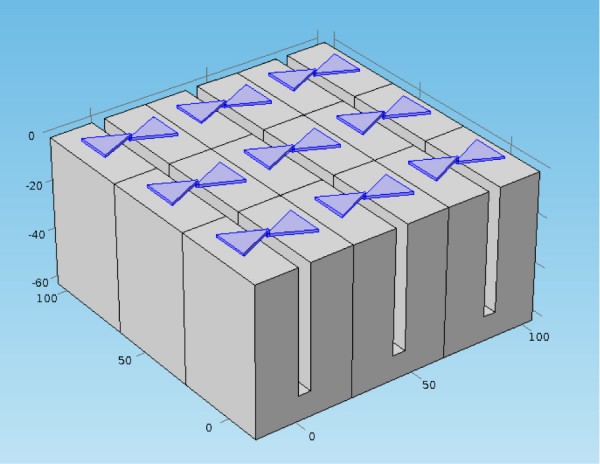
A rectenna metamaterial surface with bow-tie antennas for capture 10,000 to 100,000 times more thermal energy for conversion to DC electricity (credit: Won Park/University of Colorado)

Scientists from the University of Colorado are developing a new type of “rectenna” to efficiently “harvest” thermal emissions (waste heat) radiated from devices (a rectenna converts electromagnetic radiation to DC current).

Currently rectennas work best at low frequencies, but most heat is at higher radiation frequencies — up to the 100 THz (100 trillion cycles per second) range. So Won Park and his colleagues found a way to enhance thermal emission of hot bodies at the lower end of the spectrum (around 1 THz): by manipulating the surface of the object.

A metamaterial for engineering thermal emission

Park’s team uses software to analyze how the nanoscale topology of a surface — its bumps, holes or grooves — changes the way that electromagnetic radiation interacts with the surface. In some instances the geometry supports the formation of a wave of rippling electronic charges, called a plasmon, that hugs the surface.

“We design the surface to support a surface wave, because the presence of the wave offers a new avenue for engineering thermal emission,” Park said. For the case of optimizing thermal energy harvesting, the researchers found they could “spectrally tune” a surface to emit more radiation at 1 THz frequency.

The researchers first optimized the design, which consists of a copper plate with a regular array of tiny holes, using simulations. They then built the design in the lab and confirmed that the plate did indeed produce the type of surface waves predicted by the simulations.

The researchers also used computer modeling to design a bowtie-shaped antenna that would effectively capture the enhanced thermal emission. Simulations predict that an antenna placed near the holey surface could capture 10,000 to 100,000 times more thermal energy than an antenna in open space.

The team is in the process of experimentally testing this prediction and hopes to have new results to report soon. The results will also help the team calculate how rectenna thermal energy harvesting might compare to other ways of harvesting waste heat, such as thermoelectric materials.

The researchers described the system at the AVS 62nd International Symposium and Exhibition in San Jose, Calif. today (Monday, Oct. 19). The research is funded in part by a grant from Redwave Energy Inc.

Artificial ‘skin’ system transmits the pressure of touch

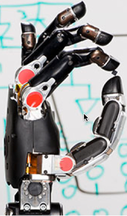
“Gimmie five”: Model robotic hand with artificial mechanoreceptors (credit: Bao Research Group, Stanford University)

Researchers have created a sensory system that mimics the ability of human skin to feel pressure and have transmitted the digital signals from the system’s sensors to the brain cells of mice. These new developments, reported in the October 16 issue of Science, could one day allow people living with prosthetics to feel sensation in their artificial limbs.

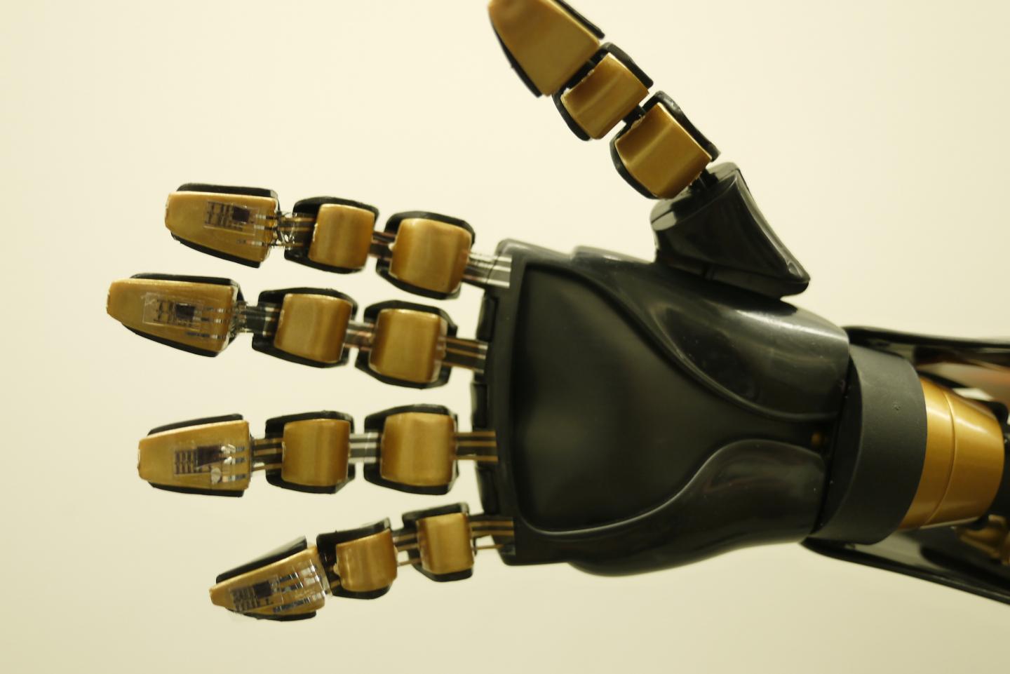
Artificial mechanoreceptors mounted on the fingers of a model robotic hand (credit: Bao Research Group, Stanford University)

The system consists of printed plastic circuits, designed to be placed on robotic fingertips. Digital signals transmitted by the system would increase as the fingertips came closer to an object, with the signal strength growing as the fingertips gripped the object tighter.

How to simulate human fingertip sensations

To simulate this human sensation of pressure, Zhenan Bao of Stanford University and her colleagues developed a number of key components that collectively allow the system to function.

As our fingers first touch an object, how we physically “feel” it depends partially on the mechanical strain that the object exerts on our skin. So the research team used a sensor with a specialized circuit that translates pressure into digital signals.

To allow the sensory system to feel the same range of pressure that human fingertips can, the team needed a highly sensitive sensor. They used carbon nanotubes in formations that are highly effective at detecting the electrical fields of inanimate objects.

Stretchable skin with flexible artificial mechanoreceptors (credit: Bao Research Group, Stanford University)

Bao noted that the printed circuits of the new sensory system would make it easy to produce in large quantities. “We would like to make the circuits with stretchable materials in the future, to truly mimic skin,” Bao said. “Other sensations, like temperature sensing, would be very interesting to combine with touch sensing.”


Abstract of A skin-inspired organic digital mechanoreceptor

Human skin relies on cutaneous receptors that output digital signals for tactile sensing in which the intensity of stimulation is converted to a series of voltage pulses. We present a power-efficient skin-inspired mechanoreceptor with a flexible organic transistor circuit that transduces pressure into digital frequency signals directly. The output frequency ranges between 0 and 200 hertz, with a sublinear response to increasing force stimuli that mimics slow-adapting skin mechanoreceptors. The output of the sensors was further used to stimulate optogenetically engineered mouse somatosensory neurons of mouse cortex in vitro, achieving stimulated pulses in accordance with pressure levels. This work represents a step toward the design and use of large-area organic electronic skins with neural-integrated touch feedback for replacement limbs.

Noninvasive imaging method can look twice as deep inside the living brain

In vivo 1.3-μm VCSEL SS-OCT imaging of a 12-week-old adult mouse with cranial window preparation. (a) Representative OCT image visualizing morphological details of the cerebral cortex and subsequent brain compartments. (b) OCT brain anatomy showing good correlation with photomicrograph of a Nissl-stained histology section of the same strain mouse brain. (credit: Allen Institute for Brain Science/Journal of Biomedical Optics)

University of Washington (UW) researchers have developed a noninvasive light-based imaging technology that can literally see inside the living brain at more than two times the depth, providing a new tool to study how diseases like dementia, Alzheimer’s, and brain tumors change brain tissue over time.

The work was reported Oct. 8 by Woo June Choi and Ruikang Wang of the UW Department of Bioengineering in the Journal of Biomedical Optics, published by SPIE, the international society for optics and photonics.

Noninvasive deep imaging

According to the authors, this new optical coherence tomography (OCT) approach to brain study may allow for examining acute and chronic morphological or functional vascular changes in the deep brain.

OCT is normally used to obtain sub-surface images of biological tissue at about the same resolution as a low-power microscope and can instantly deliver cross-section images of layers of tissue without invasive surgery or ionizing radiation. OCT images are based on light directly reflected from a sub-surface.

Widely used in clinical ophthalmology, OCT has recently been adapted for brain imaging in small animal models. Its application in neuroscience has been limited, however, because conventional OCT technology hasn’t been able to image more than 1 millimeter below the surface of biological tissue.

Portion of schematic of the 1.3-μm vertical cavity surface emitting laser (VCSEL) swept-source optical coherence tomography (SS-OCT) system. FC: optical fiber coupler; BD: dual balanced detector; DAQ: data acquisition. (credit: Woo June Choi and Ruikang K. Wang/Journal of Biomedical Optics)

In the paper, Choi and Wang describe how a new technique called “swept-source OCT” (SS-OCT) powered by a vertical-cavity surface-emitting laser (VCSEL) increases signal sensitivity, extending the imaging depth range to more than 2 millimeters. That may make it possible to do things that have been barely attempted in the OCT community, such as noninvasive imaging of the mouse hippocampus or full-length imaging of a human eye from cornea to retina.

It could also allow researchers to monitor deeper morphological changes caused by diseases such as Alzheimer’s disease and dementia, and even to study the effects of aging on the brain.


Abstract of Swept-source optical coherence tomography powered by a 1.3-μm vertical cavity surface emitting laser enables 2.3-mm-deep brain imaging in mice in vivo

We report noninvasive, in vivo optical imaging deep within a mouse brain by swept-source optical coherence tomography (SS-OCT), enabled by a 1.3-μm vertical cavity surface emitting laser (VCSEL). VCSEL SS-OCT offers a constant signal sensitivity of 105 dB throughout an entire depth of 4.25 mm in air, ensuring an extended usable imaging depth range of more than 2 mm in turbid biological tissue. Using this approach, we show deep brain imaging in mice with an open-skull cranial window preparation, revealing intact mouse brain anatomy from the superficial cerebral cortex to the deep hippocampus. VCSEL SS-OCT would be applicable to small animal studies for the investigation of deep tissue compartments in living brains where diseases such as dementia and tumor can take their toll.

Graphene nano-coils discovered to be powerful natural electromagnets

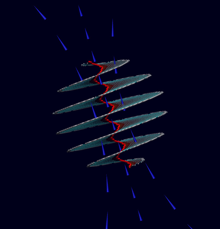
A nano-coil made of graphene could be an effective solenoid/inductor for electronic applications (credit: Yakobson Research Group/Rice University)

Rice University scientists have discovered that a widely used electronic part called a solenoid could be scaled down to nano-size with macro-scale performance.

The secret: a spiral form of atom-thin graphene that, remarkably, can be found in nature, even in common coal, according to Rice theoretical physicist Boris Yakobson and his colleagues.

The researchers determined that when a voltage is applied to such a “nano-coil,” current will flow around the helical path and produce a magnetic field, as it does in macroscale solenoids. The discovery is detailed in a new paper in the American Chemical Society journal Nano Letters.

“Perhaps this might work in reverse here: An electron current, pumped through by the applied voltage, at certain conditions may just cause the graphene spiral to spin, like a fast little electro-turbine,” Yakobson speculated.

Basic solenoid design. A current flowing through the coil generates a magnetic field, which causes a ferromagnetic plunger to be attracted or repelled. (credit: Society of Robots)

Solenoids are components with wires coiled around a metallic core. They produce a magnetic field when carrying current, turning them into electromagnets. These are widespread in electronic and mechanical devices, from circuit boards to transformers to cars.

They also serve as inductors, which are primary components in electric circuits that regulate current (the lump in power cables that feed electronic devices contains an inductor, which blocks RF interference). In their smallest form, inductors are a part of integrated circuits.

Nano-solenoids with a macro punch

While transistors get steadily smaller, basic inductors in electronics have become relatively bulky, said Fangbo Xu, a Rice alumnus and lead author of the paper. “It’s the same inside the circuits,” he said. “Commercial spiral inductors on silicon occupy excessive area. If realized, graphene nano-solenoids could change that.”

The nano-solenoids analyzed through computer models at Rice should be capable of producing powerful magnetic fields of about 1 tesla, about the same as the coils found in typical loudspeakers, according to Yakobson and his team — and about the same field strength as some MRI machines. They found the magnetic field would be strongest in the hollow, nanometer-wide cavity at the spiral’s center.

The spiral form is attributable to a simple topological trick, he said. Graphene is made of hexagonal arrays of carbon atoms. Malformed hexagons known as dislocations along one edge force the graphene to twist around itself, akin to a continuous nanoribbon that mimics a mathematical construct known as a Riemann surface.

The researchers demonstrated theoretically how energy would flow through the hexagons in nano-solenoids with edges in either armchair or zigzag formations. In one case, they determined the performance of a conventional spiral inductor of 205 microns in diameter could be matched by a nano-solenoid just 70 nanometers wide.

Multiple uses

Because graphene has no energy band gap (which gives a material semiconducting properties), electricity should move through without any barriers. But in fact, the width of the spiral and the configuration of the edges — either armchair or zigzag — influences how the current is distributed, and thus its inductive properties.

The researchers suggested it should be possible to isolate graphene screw dislocations from crystals of graphitic carbon (graphene in bulk form), but enticing graphene sheets to grow in a spiral would allow for better control of its properties, Yakobson said.

Xu suggested nano-solenoids may also be useful as molecular relays or switchable traps for magnetic molecules or radicals in chemical probes.

Co-authors are Rice graduate student Henry Yu and alumnus Arta Sadrzadeh. Yakobson is the Karl F. Hasselmann Professor of Materials Science and NanoEngineering and a professor of chemistry.

The research was supported by the Office of Naval Research’s Multidisciplinary University Research Initiative (MURI), the National Science Foundation and the Air Force Office of Scientific Research MURI.

The strongest known permanent-magnet in the world is at the Los Alamos National Laboratory campus of the National High Magnetic Field Laboratory, at 100 tesla. Does that mean 100 of these nanocoils could equal it? Comment below.


Abstract of Surfaces of Carbon as Graphene Nanosolenoids

Traditional inductors in modern electronics consume excessive areas in the integrated circuits. Carbon nanostructures can offer efficient alternatives if the recognized high electrical conductivity of graphene can be properly organized in space to yield a current-generated magnetic field that is both strong and confined. Here we report on an extraordinary inductor nanostructure naturally occurring as a screw dislocation in graphitic carbons. Its elegant helicoid topology, resembling a Riemann surface, ensures full covalent connectivity of all graphene layers, joined in a single layer wound around the dislocation line. If voltage is applied, electrical currents flow helically and thus give rise to a very large (∼1 T at normal operational voltage) magnetic field and bring about superior (per mass or volume) inductance, both owing to unique winding density. Such a solenoid of small diameter behaves as a quantum conductor whose current distribution between the core and exterior varies with applied voltage, resulting in nonlinear inductance.

Moving cooling directly to the chip for denser, longer-life electronics

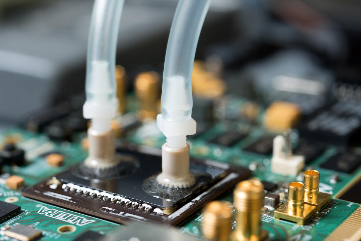
Liquid ports carry cooling water to specially designed passages etched into the backs of FPGA devices to provide more effective cooling. The liquid cooling provides a significant advantage in computing throughput. (credit: Rob Felt/Georgia Tech)

Using microfluidic passages cut directly into the backsides of production field-programmable gate array (FPGA) devices, Georgia Institute of Technology researchers have put liquid cooling where it’s needed the most: a few hundred microns away from where the transistors are operating.

Combined with connection technology that operates through structures in the cooling passages, the new technologies could allow development of denser and more powerful integrated electronic systems that would no longer require heat sinks or cooling fans on top of the integrated circuits.

Working with popular 28-nanometer FPGA devices made by Altera Corp., the researchers demonstrated a monolithically-cooled chip that can operate at temperatures more than 60 percent below those of similar air-cooled chips.

The lower temperatures can also mean longer device life and less current leakage. The cooling comes from simple de-ionized water flowing through microfluidic passages that replace the massive air-cooled heat sinks normally placed on the backs of chips.

Supported by the Defense Advanced Research Projects Agency (DARPA), the research is believed to be the first example of liquid cooling directly on an operating high-performance CMOS chip.

Liquid cooling has been used to address the heat challenges facing computing systems whose power needs have been increasing. However, existing liquid cooling technology removes heat using cold plates externally attached to fully packaged silicon chips — adding thermal resistance and reducing the heat-rejection efficiency.

In multiple tests, a liquid-cooled FPGA was operated using a custom processor architecture provided by Altera. With a water inlet temperature of approximately 20 degrees Celsius and an inlet flow rate of 147 milliliters per minute, the liquid-cooled FPGA operated at a temperature of less than 24 degrees Celsius, compared to an air-cooled device that operated at 60 degrees Celsius.

The research team chose FPGAs for their test because they provide a platform to test different circuit designs, and because FPGAs are common in many market segments, including defense. However, the same technology could also be used to cool CPUs, GPUs and other devices such as power amplifiers, according to the researchers.

In addition to improving overall cooling, the system could reduce hotspots in circuits by applying cooling much closer to the power source. Eliminating the heat sink could also allow more compact packaging of electronic devices.

The cooling research was funded by DARPA’s Microsystems Technology Office, through the ICECOOL program.


Abstract of Embedded Cooling Technologies For Densely Integrated Electronic Systems

In modern integrated systems, interconnect and thermal management technologies have become two major limitations to system performance.  In this paper we present a number of technologies to address these challenges.  First, low-loss polymer-embedded vias are demonstrated in thick wafers compatible with microfluidics.  Next, fluidic I/Os for delivery of fluid to microfluidic heat sinks are demonstrated in assembled 2.5D and 3D stacks.  Next, thermal coupling between dice in 2.5D and 3D systems is explored.  Lastly, the utility of microfluidic cooling is demonstrated through an FPGA, built in a 28nm process, with a monolithically integrated microfluidic heat sink.

Light-controlled ‘quantum Etch-a-Sketch’ could lead to advanced computers and quantum microchips

Artist’s rendition of optically defined quantum circuits in a topological insulator (credit: Peter Allen)

Penn State University and University of Chicago researchers say an accidental discovery of a “quantum Etch-a-Sketch” may lead to a new way to use beams of light to draw and erase quantum circuits, and that could lead to the next generation of advanced computers and quantum microchips.

The new technique is based on “topological insulators” (a material that behaves as an insulator in its interior but whose surface contains conducting states, meaning that electrons can only move along the surface of the material). The electrons in topological insulators have unique quantum properties that many scientists believe will be useful for developing spin-based electronics (such as disk drives) and quantum computers.

However, making even the simplest experimental circuits with topological insulators has proved difficult because traditional semiconductor engineering techniques tend to destroy their fragile quantum properties. Even a brief exposure to air can reduce their quality.

The researchers have now discovered a rewriteable “optical fabrication” process that allows them to “tune” the energy of electrons in these materials using light instead of chemicals — without ever having to touch the material itself. They used this effect to draw and erase one of the central components of a transistor — the p-n junction — in a topological insulator for the first time.

An accidental discovery

Optical fabrication (draw/erase) of a topological insulator (credit: Andrew L. Yeats et al./Science Advances)

Curiously, the scientists made the discovery when they noticed that a particular type of fluorescent light in the lab caused the surface of strontium titanate (the substrate material on which they had grown their samples) to become electrically polarized by ultraviolet light. The room lights happened to emit it at just the right wavelength. It turned out that the electric field from the polarized strontium titanate was leaking into the topological insulator layer, changing its electronic properties.

They found by intentionally focusing beams of light on their samples, they could draw electronic structures that persisted long after the light was removed. “It’s like having a sort of quantum Etch-a-Sketch in our lab,” said said David D. Awschalom, Liew Family Professor and deputy director in the Institute of Molecular Engineering at the University of Chicago. They also found that bright red light counteracted the effect of the ultraviolet light, allowing the researchers to both write (with UV) and erase (with red light).

“Instead of spending weeks in the clean room and potentially contaminating our materials, now we can sketch and measure devices for our experiments in real time,” said Awschalom. “When we’re done, we just erase it and make something else. We can do this in less than a second.”

To test whether the new technique might interfere with the unique properties of topological insulators, the team measured their samples in high magnetic fields. They found promising signatures of an effect called “weak anti-localization,” which arises from quantum interference between the different simultaneous paths that electrons can take through a material when they behave as waves.

To better understand the physics behind the effect, the researchers conducted a number of control measurements, which showed that the optical effect is not unique to topological insulators; it can also act on other materials grown on strontium titanate.

“In a way, the most exciting aspect of this work is that it should be applicable to a wide range of nanoscale materials such as complex oxides, graphene, and transition metal dichalcogenides,” said Awschalom. “It’s not just that it’s faster and easier. This effect could allow electrical tuning of materials in a wide range of optical, magnetic, and spectroscopic experiments where electrical contacts are extremely difficult or simply impossible.”

The research was published October 9, 2015 in an open-access paper in a new AAAS journal, Science Advances.


Abstract of Persistent Optical Gating of a Topological Insulator

The spin-polarized surface states of topological insulators (TIs) are attractive for applications in spintronics and quantum computing. A central challenge with these materials is to reliably tune the chemical potential of their electrons with respect to the Dirac point and the bulk bands. We demonstrate persistent, bidirectional optical control of the chemical potential of (Bi,Sb)2Te3 thin films grown on SrTiO3. By optically modulating a space-charge layer in the SrTiO3 substrates, we induce a persistent field effect in the TI films comparable to electrostatic gating techniques but without additional materials or processing. This enables us to optically pattern arbitrarily shaped p- and n-type regions in a TI, which we subsequently image with scanning photocurrent microscopy. The ability to optically write and erase mesoscopic electronic structures in a TI may aid in the investigation of the unique properties of the topological insulating phase. The gating effect also generalizes to other thin-film materials, suggesting that these phenomena could provide optical control of chemical potential in a wide range of ultrathin electronic systems.