Hybrid bio-robotic system models physics of human leg locomotion

Schematic of bio-robotic modeling system (credit: Benjamin D. Robertson and Gregory S. Sawicki/PNAS)

North Carolina State University (NC State) researchers have developed a bio-inspired system that models how human leg locomotion works, by using a computer-controlled nerve stimulator (acting as the spinal cord) to activate a biological muscle-tendon.

The findings could help design robotic devices that begin to merge human and machine to assist human locomotion, serving as prosthetic systems for people with mobility impairments or exoskeletons for increasing the abilities of able-bodied individuals.

The model is based on the natural spring-like physics (mass, stiffness, and leverage) of the ankle’s primary muscle-tendon unit (using a bullfrog’s muscle). The system used a feedback-controlled servomotor, simulating the inertial/gravitational environment of terrestrial gait.

Tuning for natural resonance

The research showed that the natural resonance* of the system is a likely mechanism behind springy leg behavior during locomotion, according to Gregory Sawicki, associate professor at NC State and University of North Carolina at Chapel Hill Joint Department of Biomedical Engineering. He is also co-author of a paper on the work published in Proceedings of the National Academy of Sciences.

In this case, the electrical system — the body’s nervous system — drives the mechanical system (the leg’s muscle-tendon unit) at a frequency that provides maximum power output.

The researchers found that by matching the stimulation frequency to the natural resonance frequency of the passive biomechanical system, muscle-tendon interactions (resulting in spring-like behavior) occur naturally and do not require closed-loop neural control — simplifying system design.

“In locomotion, resonance comes from tuning the interaction between the nervous system and the leg so they work together,” said Sawicki. “It turns out that if I know the mass, leverage, and stiffness of a muscle-tendon unit, I can tell you exactly how often I should stimulate it to get resonance in the form of spring-like, elastic behavior.”

“In the end, we found that the same simple underlying principles that govern resonance in simple mechanical systems also apply to these extraordinarily complicated physiological systems,” said Temple University post-doctoral researcher Ben Robertson, corresponding author of the paper.

“This outcome points to mechanical resonance as an underlying principle governing muscle-tendon interactions and provides a physiology-based framework for understanding how mechanically simple elastic limb behavior may emerge from a complex biological system comprised of many simultaneously tuned muscle-tendons within the lower limb,” the researchers conclude in the paper.

* NC State biomedical engineer Greg Sawicki likened resonance tuning to interacting with a slinky toy. “When you get it oscillating well, you hardly have to move your hand — it’s the timing of the interaction forces that matters.


Abstract of Unconstrained muscle-tendon workloops indicate resonance tuning as a mechanism for elastic limb behavior during terrestrial locomotion

In terrestrial locomotion, there is a missing link between observed spring-like limb mechanics and the physiological systems driving their emergence. Previous modeling and experimental studies of bouncing gait (e.g., walking, running, hopping) identified muscle-tendon interactions that cycle large amounts of energy in series tendon as a source of elastic limb behavior. The neural, biomechanical, and environmental origins of these tuned mechanics, however, have remained elusive. To examine the dynamic interplay between these factors, we developed an experimental platform comprised of a feedback-controlled servo-motor coupled to a biological muscle-tendon. Our novel motor controller mimicked in vivo inertial/gravitational loading experienced by muscles during terrestrial locomotion, and rhythmic patterns of muscle activation were applied via stimulation of intact nerve. This approach was based on classical workloop studies, but avoided predetermined patterns of muscle strain and activation—constraints not imposed during real-world locomotion. Our unconstrained approach to position control allowed observation of emergent muscle-tendon mechanics resulting from dynamic interaction of neural control, active muscle, and system material/inertial properties. This study demonstrated that, despite the complex nonlinear nature of musculotendon systems, cyclic muscle contractions at the passive natural frequency of the underlying biomechanical system yielded maximal forces and fractions of mechanical work recovered from previously stored elastic energy in series-compliant tissues. By matching movement frequency to the natural frequency of the passive biomechanical system (i.e., resonance tuning), muscle-tendon interactions resulting in spring-like behavior emerged naturally, without closed-loop neural control. This conceptual framework may explain the basis for elastic limb behavior during terrestrial locomotion.

A battery alternative to costly, rare lithium

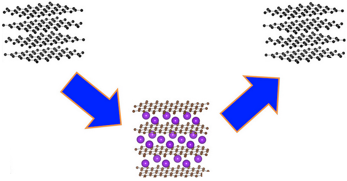
Potassium ions (purple) are compatible with graphite electrodes (black) and can function in a charge-discharge cycle, chemists have now shown (credit: Oregon State University)

Overturning nearly a century of a scientific dogma, Oregon State University chemists have now shown that  potassium could potentially replace rare, costly lithium in a new potassium-ion battery.

“For decades, people have assumed that potassium couldn’t work with graphite or other bulk carbon anodes in a battery,” said Xiulei (David) Ji, the lead author of the study and an assistant professor of chemistry in the College of Science at Oregon State University. “That assumption is incorrect,” he said. “It’s really shocking that no one ever reported on this issue for 83 years.”

The findings are important, the researchers say, because they open some new alternatives for batteries that can work with well-established, inexpensive graphite as the anode (the high-energy reservoir of electrons).

Lithium is quite rare, found in only 0.0017 percent, by weight, of the Earth’s crust. Because of that, it’s comparatively expensive, and also difficult to recycle.

Cost, availability problems with lithium

“The cost-related problems with lithium are sufficient that you won’t really gain much with economies of scale,” Ji said. “With most products, as you make more of them, the cost goes down. With lithium the reverse may be true in the near future. So we have to find alternatives.”

That alternative, he said, may be potassium, which is 880 times more abundant in the Earth’s crust than lithium. The new findings show that it can work effectively with graphite or soft carbon in the anode of an electrochemical battery.

“It’s safe to say that the energy density (amount of electrical power per unit volume) of a potassium-ion battery may never exceed that of lithium-ion batteries,” he said. But potassium-ion batteries may provide a “long cycling life, a high power density [ability to discharge quickly], a lot lower cost, and be ready to take the advantage of the existing manufacturing processes of carbon anode materials.”

Electrical energy storage in batteries is essential not only for consumer products such as cell phones and computers, but also in transportation, industry power backup, micro-grid storage, and for the wider use of renewable energy.

The Journal of the American Chemical Society published the findings from this discovery, which was supported by the U.S. Department of Energy. A patent is pending on the new technology.


Abstract of Carbon Electrodes for K-Ion Batteries

We for the first time report electrochemical potassium insertion in graphite in a nonaqueous electrolyte, which can exhibit a high reversible capacity of 273 mAh/g. Ex situ XRD studies confirm that KC36, KC24, and KC8 sequentially form upon potassiation, whereas depotassiation recovers graphite through phase transformations in an opposite sequence. Graphite shows moderate rate capability and relatively fast capacity fading. To improve the performance of carbon K-ion anodes, we synthesized a nongraphitic soft carbon that exhibits cyclability and rate capability much superior to that of graphite. This work may open up a new paradigm toward rechargeable K-ion batteries.

A realistic bio-inspired robotic finger

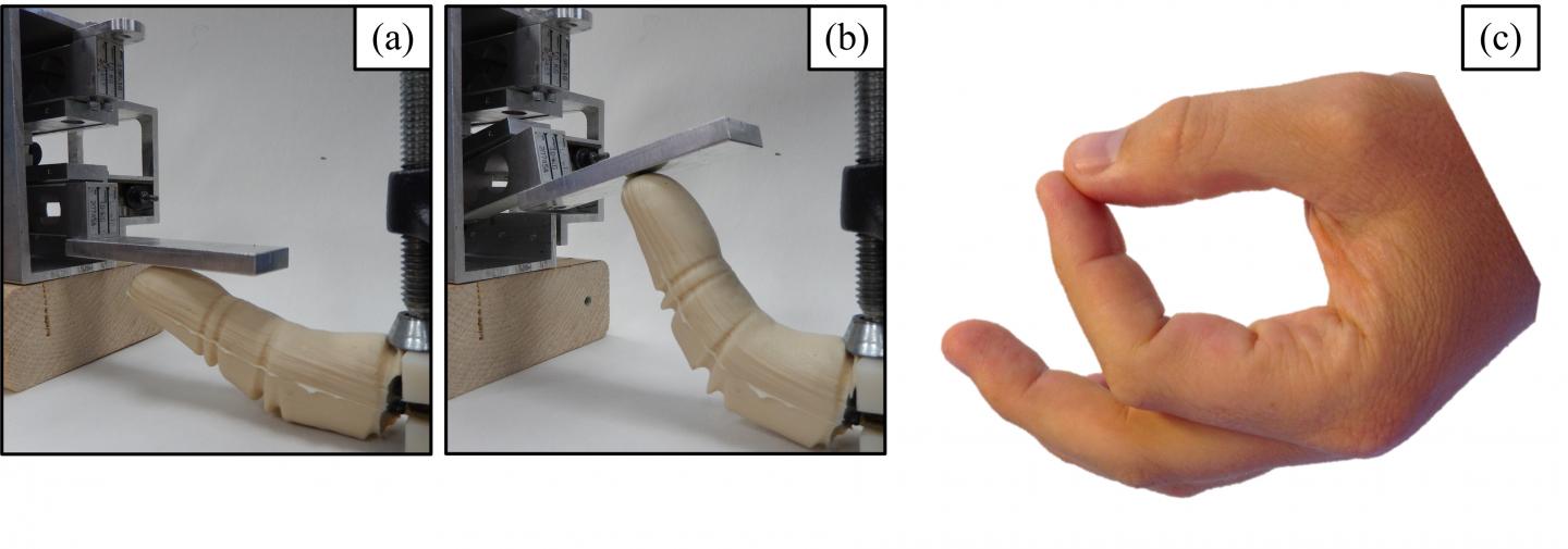
Heating and cooling a 3D-printed shape memory alloy to operate a robotic finger (credit: Florida Atlantic University/Bioinspiration & Biomimetics)

A realistic 3D-printed robotic finger using a shape memory alloy (SMA) and a unique thermal training technique has been developed by Florida Atlantic University assistant professor Erik Engeberg, Ph.D.

“We have been able to thermomechanically train our robotic finger to mimic the motions of a human finger, like flexion and extension,” said Engeberg. “Because of its light weight, dexterity and strength, our robotic design offers tremendous advantages over traditional mechanisms, and could ultimately be adapted for use as a prosthetic device, such as on a prosthetic hand.”

Most robotic parts used today are rigid, have a limited range of motion and don’t look lifelike.

In the study, described in an open-access article in the journal Bioinspiration & Biomimetics, Engeberg and his team used a resistive heating process called “Joule” heating that involves the passage of electric currents through a conductor that releases heat.

How to create a robotic finger

  • The researchers first downloaded a 3-D computer-aided design (CAD) model of a human finger from the Autodesk 123D website (under creative commons license).
  • With a 3-D printer, they created the inner and outer molds that housed a flexor and extensor actuator and a position sensor. The extensor actuator takes a straight shape when it’s heated and the flexor actuator takes a curved shape when heated.
  • They used SMA plates and a multi-stage casting process to assemble the finger.
  • Electric currents flow through each SMA actuator from an electric power source at the base of the finger as a heating and cooling process to operate the robotic finger.

Results from the study showed a rapid flexing and extending motion of the finger and ability to recover its trained shape accurately and completely, confirming the biomechanical basis of its trained shape.

Initial use in underwater robotics

“Because SMAs require a heating process and cooling process, there are challenges with this technology, such as the lengthy amount of time it takes for them to cool and return to their natural shape, even with forced air convection,” said Engeberg. So they used the technology for underwater robotics, which would provide a rapid-cooling environment.

Engeberg used thermal insulators at the fingertip, which were kept open to facilitate water flow inside the finger. As the finger flexed and extended, water flowed through the inner cavity within each insulator to cool the actuators.

“Because our robotic finger consistently recovered its thermomechanically trained shape better than other similar technologies, our underwater experiments clearly demonstrated that the water cooling component greatly increased the operational speed of the finger,” said Engeberg.

Undersea applications using Engeberg’s new technology could help to address some of the difficulties and challenges humans encounter while working in ocean depths.


FAU – BioRobotics Lab | Bottle Pick and Drop Demo UR10 and Shadow Hand


FAU – BioRobotics Lab | Simultaneous Grasp Synergies Controlled by EMG


FAU – BioRobotics Lab | Shadow Hand and UR10 – Grab Bottle, Pour Liquid


Abstract of Anthropomorphic finger antagonistically actuated by SMA plates

Most robotic applications that contain shape memory alloy (SMA) actuators use the SMA in a linear or spring shape. In contrast, a novel robotic finger was designed in this paper using SMA plates that were thermomechanically trained to take the shape of a flexed human finger when Joule heated. This flexor actuator was placed in parallel with an extensor actuator that was designed to straighten when Joule heated. Thus, alternately heating and cooling the flexor and extensor actuators caused the finger to flex and extend. Three different NiTi based SMA plates were evaluated for their ability to apply forces to a rigid and compliant object. The best of these three SMAs was able to apply a maximum fingertip force of 9.01N on average. A 3D CAD model of a human finger was used to create a solid model for the mold of the finger covering skin. Using a 3D printer, inner and outer molds were fabricated to house the actuators and a position sensor, which were assembled using a multi-stage casting process. Next, a nonlinear antagonistic controller was developed using an outer position control loop with two inner MOSFET current control loops. Sine and square wave tracking experiments demonstrated minimal errors within the operational bounds of the finger. The ability of the finger to recover from unexpected disturbances was also shown along with the frequency response up to 7 rad s−1. The closed loop bandwidth of the system was 6.4 rad s−1 when operated intermittently and 1.8 rad s−1 when operated continuously.

A new way to create spintronic magnetic information storage

A magnetized cobalt disk (red) placed atop a thin cobalt-palladium film (light purple background) can be made to confer its own ringed configuration of magnetic moments (orange arrows) to the film below, creating a skyrmion in the film (purple arrows). The skyrmion might be usable in computer data storage systems. (credit: Dustin Gilbert / NIST)

Exotic ring-shaped magnetic effects called “skyrmions*” could be the basis for a new type of nonvolatile magnetic computer data storage, replacing current hard-drive technology, according to a team of researchers at the National Institute of Standards and Technology (NIST) and several universities.

Skyrmions have the advantage of operating at magnetic fields that are several orders of magnitude weaker, but have worked at only very low temperatures until now. The research breakthrough was the discovery of a practical way to create and access magnetic skyrmions, and under ambient room-temperature conditions.

The skrymion effect refers to extreme conditions in which certain magnetic materials can develop spots where the magnetic moments** curve and twist, forming a winding, ring-like configuration. To achieve that, the physicists placed arrays of tiny magnetized cobalt disks atop a thin film made of cobalt and palladium. That protects them from outside influence, meaning the data they store would not be corrupted easily.

But “seeing” these skyrmion configurations underneath was a challenge. The team solved that by using neutrons to see through the disk.

That discovery has implications for spintronics (using magnetic spin to store data). “The advantage [with skyrmions] is that you’d need way less power to push them around than any other method proposed for spintronics,” said NIST’s Dustin Gilbert. “What we need to do next is figure out how to make them move around.”

Physicists at the University of California, Davis; University of Maryland, College Park; University of California, Santa Cruz; and Lawrence Berkeley National Laboratory were also involved in the study.

* Named after the physicist who proposed them. 

** The force that a magnet can exert on electric currents and the torque that a magnetic field will exert on it.


Abstract of Realization of ground-state artificial skyrmion lattices at room temperature

The topological nature of magnetic skyrmions leads to extraordinary properties that provide new insights into fundamental problems of magnetism and exciting potentials for novel magnetic technologies. Prerequisite are systems exhibiting skyrmion lattices at ambient conditions, which have been elusive so far. Here, we demonstrate the realization of artificial Bloch skyrmion lattices over extended areas in their ground state at room temperature by patterning asymmetric magnetic nanodots with controlled circularity on an underlayer with perpendicular magnetic anisotropy (PMA). Polarity is controlled by a tailored magnetic field sequence and demonstrated in magnetometry measurements. The vortex structure is imprinted from the dots into the interfacial region of the underlayer via suppression of the PMA by a critical ion-irradiation step. The imprinted skyrmion lattices are identified directly with polarized neutron reflectometry and confirmed by magnetoresistance measurements. Our results demonstrate an exciting platform to explore room-temperature ground-state skyrmion lattices.

Gartner identifies the top 10 strategic IT technology trends for 2016

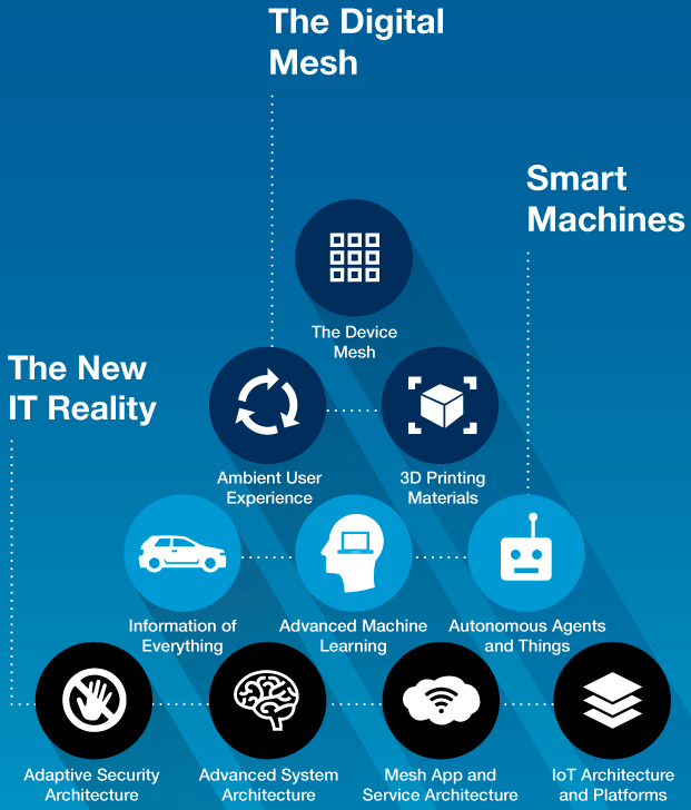
Top 10 strategic trends 2016 (credit: Gartner, Inc.)

At the Gartner Symposium/ITxpo today (Oct. 8), Gartner, Inc. highlighted the top 10 technology trends that will be strategic for most organizations in 2016 and will shape digital business opportunities through 2020.

The Device Mesh

The device mesh refers to how people access applications and information or interact with people, social communities, governments and businesses. It includes mobile devices, wearable, consumer and home electronic devices, automotive devices, and environmental devices, such as sensors in the Internet of Things (IoT), allowing for greater cooperative interaction between devices.

Ambient User Experience

The device mesh creates the foundation for a new continuous and ambient user experience. Immersive environments delivering augmented and virtual reality hold significant potential but are only one aspect of the experience. The ambient user experience preserves continuity across boundaries of device mesh, time and space. The experience seamlessly flows across a shifting set of devices — such as sensors, cars, and even factories — and interaction channels blending physical, virtual and electronic environment as the user moves from one place to another.

3D Printing Materials

Advances in 3D printing will drive user demand and a compound annual growth rate of 64.1 percent for enterprise 3D-printer shipments through 2019, which will require a rethinking of assembly line and supply chain processes to exploit 3D printing.

Information of Everything

Everything in the digital mesh produces, uses and transmits information, including sensory and contextual information. “Information of everything” addresses this influx with strategies and technologies to link data from all these different data sources. Advances in semantic tools such as graph databases as well as other emerging data classification and information analysis techniques will bring meaning to the often chaotic deluge of information.

Advanced Machine Learning

In advanced machine learning, deep neural nets (DNNs) move beyond classic computing and information management to create systems that can autonomously learn to perceive the world on their own, making it possible to address key challenges related to the information of everything trend.

DNNs (an advanced form of machine learning particularly applicable to large, complex datasets) is what makes smart machines appear “intelligent.” DNNs enable hardware- or software-based machines to learn for themselves all the features in their environment, from the finest details to broad sweeping abstract classes of content. This area is evolving quickly, and organizations must assess how they can apply these technologies to gain competitive advantage.

Autonomous Agents and Things

Machine learning gives rise to a spectrum of smart machine implementations — including robots, autonomous vehicles, virtual personal assistants (VPAs) and smart advisors — that act in an autonomous (or at least semiautonomous) manner.

VPAs such as Google Now, Microsoft’s Cortana, and Apple’s Siri are becoming smarter and are precursors to autonomous agents. The emerging notion of assistance feeds into the ambient user experience in which an autonomous agent becomes the main user interface. Instead of interacting with menus, forms and buttons on a smartphone, the user speaks to an app, which is really an intelligent agent.

Adaptive Security Architecture

The complexities of digital business and the algorithmic economy combined with an emerging “hacker industry” significantly increase the threat surface for an organization. Relying on perimeter defense and rule-based security is inadequate, especially as organizations exploit more cloud-based services and open APIs for customers and partners to integrate with their systems. IT leaders must focus on detecting and responding to threats, as well as more traditional blocking and other measures to prevent attacks. Application self-protection, as well as user and entity behavior analytics, will help fulfill the adaptive security architecture.

Advanced System Architecture

The digital mesh and smart machines require intense computing architecture demands to make them viable for organizations. Providing this required boost are high-powered and ultraefficient neuromorphic (brain-like) architectures fueled by GPUs (graphic processing units) and field-programmable gate arrays (FPGAs). There are significant gains to this architecture, such as being able to run at speeds of greater than a teraflop with high-energy efficiency.

Mesh App and Service Architecture

Monolithic, linear application designs (e.g., the three-tier architecture) are giving way to a more loosely coupled integrative approach: the apps and services architecture. Enabled by software-defined application services, this new approach enables Web-scale performance, flexibility and agility. Microservice architecture is an emerging pattern for building distributed applications that support agile delivery and scalable deployment, both on-premises and in the cloud. Containers are emerging as a critical technology for enabling agile development and microservice architectures. Bringing mobile and IoT elements into the app and service architecture creates a comprehensive model to address back-end cloud scalability and front-end device mesh experiences. Application teams must create new modern architectures to deliver agile, flexible and dynamic cloud-based applications that span the digital mesh.

Internet of Things Platforms

IoT platforms complement the mesh app and service architecture. The management, security, integration and other technologies and standards of the IoT platform are the base set of capabilities for building, managing, and securing elements in the IoT. The IoT is an integral part of the digital mesh and ambient user experience and the emerging and dynamic world of IoT platforms is what makes them possible.

* Gartner defines a strategic technology trend as one with the potential for significant impact on the organization. Factors that denote significant impact include a high potential for disruption to the business, end users or IT, the need for a major investment, or the risk of being late to adopt. These technologies impact the organization’s long-term plans, programs and initiatives.

DARPA selects research teams for its ElectRx neuron-sensing/stimulation program

DARPA announced Monday (Oct. 5, 2015) that it has selected seven teams of researchers to begin work on a radical new approach to healing called Electrical Prescriptions (ElectRx). It would involve a system that stimulates peripheral nerves to modulate functions in the brain, spinal cord, and internal organs, according to program manager Doug Weber.

DARPA envisions a closed-loop system aimed at monitoring and treating conditions such as chronic pain, inflammatory disease, post-traumatic stress, and other illnesses that may not be responsive to traditional treatments, using optical, acoustic, electromagnetic, or engineered biology strategies to achieve precise targeting, possibly at single-axon resolution.

Pacemakers for other organs

The oldest and simplest example of this concept is the cardiac pacemaker, which uses brief pulses of electricity to stimulate the heart to beat at a healthy rate. DARPA aims to extend this concept to other organs, like the spleen, and treat inflammatory diseases such as rheumatoid arthritis.

Fighting inflammation may also provide new treatments for depression, which growing evidence suggests might be caused in part by excess levels of inflammatory biomolecules. Peripheral nerve stimulation may also be used to regulate production of neurochemicals that regulate learning and memory in the brain, offering new treatments for post-traumatic stress and other mental health disorders.

In phase 1, the ElectRx program will focus on fundamental studies to map the neural circuits governing the physiology of diseases of interest to DARPA, and also on preliminary development of novel, minimally invasive neural and bio-interface technologies with unprecedented levels of precision, targeting, and scale.

The teams

The seven teams include a mix of first-time and prior DARPA performers.

For example, an MIT team led by Polina Anikeeva will aim to advance its research in stimulating brain tissue using external magnetic fields and injected magnetic nanoparticles to treat neurological diseases such as Parkinson’s disease, replacing surgically implanted electrodes, as KurzweilAI reported in March. When exposed to a low-frequency (100 kHz — 1 MHz) external alternating magnetic field — which can penetrate deep inside biological tissues — these nanoparticles rapidly heat up and trigger heat-sensitive capsaicin (the “hot” in peppers) receptors to stimulate neurons.


MIT | Wireless brain stimulation

The other teams are:

  • Circuit Therapeutics (Menlo Park, Calif.), a start-up co-founded by Stanford University scientists Karl Deisseroth and Scott Delp, plans to further develop its experimental optogenetic methods for treating neuropathic pain, building toward testing in animal models first.
  • A team at Columbia University (New York), led by Elisa Konofagou, will pursue fundamental science to support the use of non-invasive, targeted ultrasound for neuromodulation. The team aims to elucidate the underlying mechanisms that may make ultrasound an option for chronic intervention, including activation and inhibition of nerves.
  • A team at the Florey Institute of Neuroscience and Mental Health (Parkville, Australia), led by John Furness, will seek to map the nerve pathways that underlie intestinal inflammation, with a focus on determining the correlations between animal models and human neural circuitry. They will also explore the use of neurostimulation technologies based on the cochlear implant — developed by Cochlear, Inc. to treat hearing loss but adapted to modulate activity of the vagus nerve in response to biofeedback signals — as a possible treatment for inflammatory bowel disease.
  • A team at the Johns Hopkins University (Baltimore), led by Jiande Chen, aims to explore the root mechanisms of inflammatory bowel disease and the impact of sacral nerve stimulation on its progression. The team will apply a first-of-its-kind approach to visualize intestinal responses to neuromodulation in animal models.
  • A team at Purdue University (West Lafayette, Ind.), led by Pedro Irazoqui, will leverage an existing collaboration with Cyberonics to study inflammation of the gastrointestinal tract and its responsiveness to vagal nerve stimulation through the neck. Validation of the mechanistic insights that emerge from the effort will take place in pre-clinical models in which novel neuromodulation devices will be applied to reduce inflammation in a feedback-controlled manner. Later stages of the effort could advance the design of clinical neuromodulation devices.
  • A team at the University of Texas, Dallas, led by Robert Rennaker and Michael Kilgard, will examine the use of vagal nerve stimulation to induce neural plasticity for the treatment of post-traumatic stress. As envisioned, stimulation could enhance learned behavioral responses that reduce fear and anxiety when presented with traumatic cues. Dr. Rennaker is a U.S. Marine Corps veteran who served in Liberia, Kuwait and Yugoslavia.

Vertical ‘light antennas’ grown from organic semiconductor crystals

In full bloom: A scanning electron microscopy image of a vertical tetraanaline semiconductor crystal (credit: Jessica Wang)

Materials scientists from the California NanoSystems Institute at UCLA have discovered a way to make organic (carbon-based) semiconductors more powerful and efficient by creating “light antennas.” The thin, pole-like devices could absorb light from all directions, an improvement over today’s wide, flat panels that can only absorb light from one surface.

The breakthrough was in creating an improved structure for one type of organic semiconductor: a building block of a conductive polymer called tetraaniline (TANI). The scientists showed for the first time that tetraaniline crystals could be grown vertically.

The study, led by Richard Kaner, distinguished professor of chemistry and biochemistry and materials science and engineering, was recently published online by the journal ACS Nano.

Growing vertical organic semiconductors

Scanning electron microscope image showing TANI crystals oriented vertically based on graphene (credit: Yue Wang et al./ACS Nano)

The UCLA team grew the tetraaniline crystals vertically from a substrate made of graphene, so the crystals stood up like spikes instead of lying flat as they do when produced using current techniques. Scientists had previously grown crystals vertically in inorganic semiconducting materials, including silicon, but doing it in organic materials has been more difficult.

Tetraaniline is a desirable material for semiconductors because of its particular electrical and chemical properties, which are determined by the orientation of very small crystals it contains. Devices such as solar cells, photosensors, and supercapacitors would work better if the crystals grew vertically because vertical crystals can be packed more densely in the semiconductor, making it more powerful and more efficient at controlling electrical current.

Kaner and his colleagues also developed a one-step method for growing highly ordered, vertically aligned crystals for a variety of organic semiconductors using the same graphene substrate. “This technique enables us to pattern crystals wherever we want,” he said. “You could make electronic devices from these semiconductor crystals and grow them precisely in intricate patterns required for the device you want, such as thin-film transistors or light-emitting diodes.”

The research was supported by the Boeing Company, the National Science Foundation, the U.S. Department of Energy, and the Defense Threat Reduction Agency.


Abstract of Graphene-Assisted Solution Growth of Vertically Oriented Organic Semiconducting Single Crystals

Vertically oriented structures of single crystalline conductors and semiconductors are of great technological importance due to their directional charge carrier transport, high device density, and interesting optical properties. However, creating such architectures for organic electronic materials remains challenging. Here, we report a facile, controllable route for producing oriented vertical arrays of single crystalline conjugated molecules using graphene as the guiding substrate. The arrays exhibit uniform morphological and crystallographic orientations. Using an oligoaniline as an example, we demonstrate this method to be highly versatile in controlling the nucleation densities, crystal sizes, and orientations. Charge carriers are shown to travel most efficiently along the vertical interfacial stacking direction with a conductivity of 12.3 S/cm in individual crystals, the highest reported to date for an aniline oligomer. These crystal arrays can be readily patterned and their current harnessed collectively over large areas, illustrating the promise for both micro- and macroscopic device applications.

Method to replace silicon with carbon nanotubes developed by IBM Research

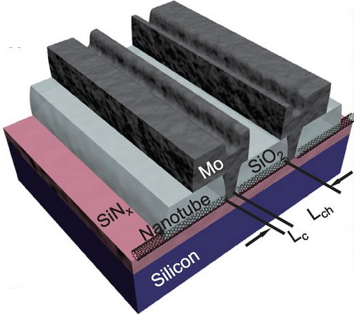
Schematic of a set of molybdenum (M0) end-contacted nanotube transistors (credit: Qing Cao et al./Science)

IBM Research has announced a “major engineering breakthrough” that could lead to carbon nanotubes replacing silicon transistors in future computing technologies.

As transistors shrink in size, electrical resistance increases within the contacts, which impedes performance. So IBM researchers invented a metallurgical process similar to microscopic welding that chemically binds the contact’s metal (molybdenum) atoms to the carbon atoms at the ends of nanotubes.

The new method promises to shrink transistor contacts without reducing performance of carbon-nanotube devices, opening a pathway to dramatically faster, smaller, and more powerful computer chips beyond the capabilities of traditional silicon semiconductors.

“This is the kind of breakthrough that we’re committed to making at IBM Research via our $3 billion investment over 5 years in research and development programs aimed a pushing the limits of chip technology,” said Dario Gil, VP, Science & Technology, IBM Research. “Our aim is to help IBM produce high-performance systems capable of handling the extreme demands of new data analytics and cognitive computing applications.”

The development was reported today in the October 2 issue of the journal Science.

Overcoming contact resistance

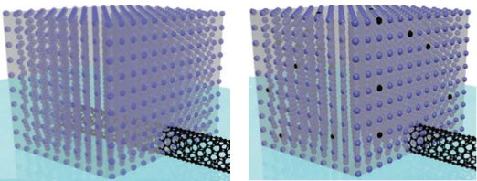
Schematic of carbon nanotube transistor contacts. Left: High-resistance side-bonded contact, where the single-wall nanotube (SWNT) (black tube) is partially covered by the metal molybdenum (Mo) (purple dots). Right: low-resistance end-bonded contact, where the SWNT is attached to the molybdenum electrode through carbide bonds, while the carbon atoms (black dots) from the originally covered portion of the SWNT uniformly diffuse out into the Mo electrode (credit: Qing Cao et al./Science)

The new “end-bonded contact scheme” allows carbon-nanotube contacts to be shrunken down to below 10 nanometers without deteriorating performance. IBM says the scheme could overcome contact resistance challenges all the way to the 1.8 nanometer node and replace silicon with carbon nanotubes.

Silicon transistors have been made smaller year after year, but they are approaching a point of physical limitation. With Moore’s Law running out of steam, shrinking the size of the transistor — including the channels and contacts — without compromising performance has been a challenge for researchers for decades.

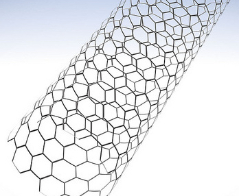
Single wall carbon nanotube (credit: IBM)

IBM has previously shown that carbon nanotube transistors can operate as excellent switches at channel dimensions of less than ten nanometers, which is less than half the size of today’s leading silicon technology. Electrons in carbon transistors can move more easily than in silicon-based devices and use less power.

Carbon nanotubes are also flexible and transparent, making them useful for flexible and stretchable electronics or sensors embedded in wearables.

IBM acknowledges that several major manufacturing challenges still stand in the way of commercial devices based on nanotube transistors.

Earlier this summer, IBM unveiled the first 7 nanometer node silicon test chip, pushing the limits of silicon technologies.


A promising new 2-D semiconductor material

Ultrathin sheets of a new 2-D hybrid perovskite are square-shaped and relatively large in area, properties that should facilitate their integration into future electronic devices (credit: Peidong Yang, Berkeley Lab)

The first atomically thin 2D sheets of organic-inorganic hybrid perovskites have been created by Lawrence Berkeley National Laboratory (Berkeley Lab) researchers, adding to the growing list of two-dimensional semiconductors, such as graphene, boron nitride, and molybdenum disulfide, whose unique electronic properties make them potential successors to silicon in future devices.

However, unlike the other contenders, which are covalent semiconductors, these 2D hybrid perovskites are ionic materials, which gives them special properties of their own.

Traditional perovskites are typically metal-oxide materials that display a wide range of electromagnetic properties, including ferroelectricity and piezoelectricity, superconductivity and colossal magnetoresistance. As KurzweilAI has reported, perovskites have been solution-processed recently into thin films or bulk crystals for photovoltaic devices, reaching 20-percent power conversion efficiency; and have been used to create lower-cost, high-brightness LEDs.

2D atomically thin nanostructures

The new ultrathin sheets are of high quality, large in area, and square-shaped. They also exhibited efficient photoluminescence, color-tunability, and a unique structural relaxation not found in covalent semiconductor sheets.

“We believe this is the first example of 2D atomically thin nanostructures made from ionic materials,” says Peidong Yang, a chemist with Berkeley Lab’s Materials Sciences Division and world authority on nanostructures, who first came up with the idea for this research some 20 years ago.

“The results of our study open up opportunities for fundamental research on the synthesis and characterization of atomically thin 2D hybrid perovskites and introduce a new family of 2D solution-processed semiconductors for nanoscale optoelectronic devices, such as field effect transistors and photodetectors.”

Yang, who also holds appointments with the University of California (UC) Berkeley and is a co-director of the Kavli Energy NanoScience Institute (Kavli-ENSI), is the corresponding author of a paper describing this research in the journal Science. 

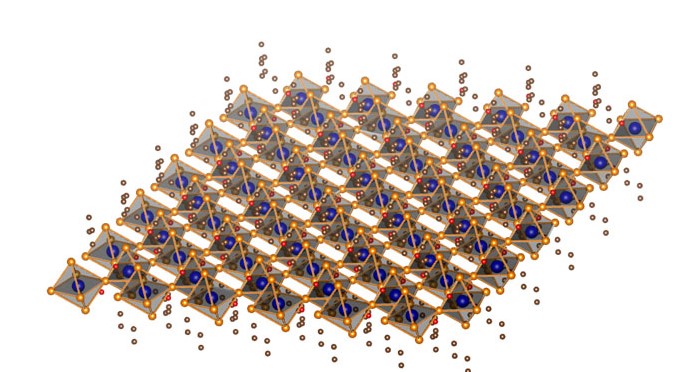
Structural illustration of a single layer of a 2D hybrid perovskite (C4H9NH3)2PbBr4), an ionic material with different properties than 2D covalent semiconductors (credit: Peidong Yang, Berkeley Lab)


Abstract of Atomically thin two-dimensional organic-inorganic hybrid perovskites

Organic-inorganic hybrid perovskites, which have proved to be promising semiconductor materials for photovoltaic applications, have been made into atomically thin two-dimensional (2D) sheets. We report the solution-phase growth of single- and few-unit-cell-thick single-crystalline 2D hybrid perovskites of (C4H9NH3)2PbBr4 with well-defined square shape and large size. In contrast to other 2D materials, the hybrid perovskite sheets exhibit an unusual structural relaxation, and this structural change leads to a band gap shift as compared to the bulk crystal. The high-quality 2D crystals exhibit efficient photoluminescence, and color tuning could be achieved by changing sheet thickness as well as composition via the synthesis of related materials.

New prosthesis bypasses brain damage by re-encoding memories

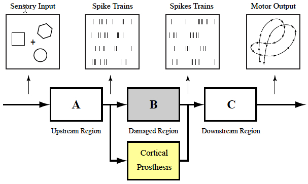
Cortical memory prosthesis uses internal brain signals (e.g., spike
trains) as inputs and outputs, bypassing damaged region (Dong Song et al.)

A brain prosthesis designed to help individuals suffering from memory loss has been developed by researchers at USC and Wake Forest Baptist Medical Center.

The prosthesis, which uses a small array of electrodes implanted into the brain, has performed well in laboratory testing in animals and is currently being evaluated in human patients.

The device builds on decades of research by Ted Berger and relies on a new algorithm created by Dong Song, both of the USC Viterbi School of Engineering. The development also builds on more than a decade of collaboration with Sam Deadwyler and Robert Hampson of the Department of Physiology & Pharmacology of Wake Forest Baptist, who have collected the neural data used to construct the models and algorithms.

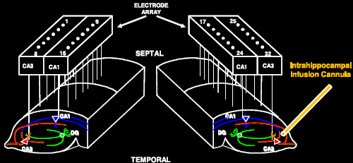
electrode_array

Electrode array for monitoring and duplicating hippocampus neuron activity (credit: T. Berger et al./Journal of Neural Engineering)

When your brain receives a sensory input, it creates a memory in the form of a complex electrical signal that travels through multiple regions of the hippocampus, the memory center of the brain. At each region, the signal is re-encoded until it reaches the final region as a wholly different signal that is sent off for long-term storage.

If there’s damage at any region that prevents this translation, there is the possibility that long-term memory will not be formed. That’s why an individual with hippocampal damage (for example, due to Alzheimer’s disease) can recall events from a long time ago — things that were already translated into long-term memories before the brain damage occurred — but have difficulty forming new long-term memories.

Bypassing a damaged hippocampal section

Song and Berger found a way to accurately mimic how a memory is translated from short-term memory into long-term memory, using data obtained by Deadwyler and Hampson, first from animals, and then from humans. Their prosthesis is designed to bypass a damaged hippocampal section and provide the next region with the correctly translated memory.

That’s despite the fact that there is currently no way of “reading” a memory just by looking at its electrical signal. “It’s like being able to translate from Spanish to French without being able to understand either language,” Berger said.

Their research was presented at the 37th Annual International Conference of the IEEE Engineering in Medicine and Biology Society in Milan on August 27, 2015.

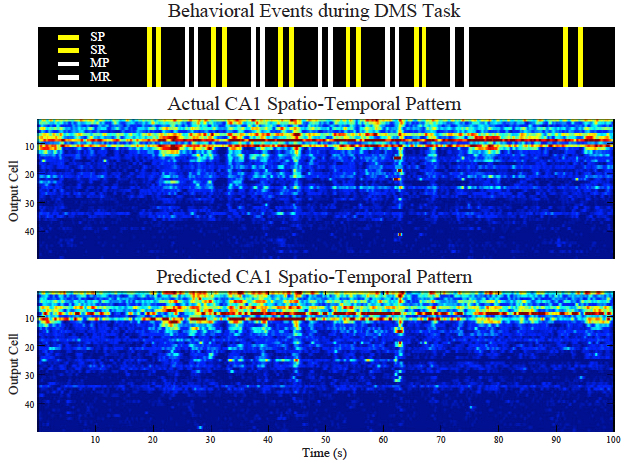
Predicting CA1 spatio-temporal patterns from CA3 spatio-temporal patterns with the sparse MIMO model. SP: sample presentation; SR: sample response; MP: match presentation; MR: match response. (Dong Song et al.)

The effectiveness of the model was tested by the USC and Wake Forest Baptist teams. With the permission of patients who had electrodes implanted in their hippocampi to treat chronic seizures, Hampson and Deadwyler read the electrical signals created during memory formation at two regions of the hippocampus, then sent that information to Song and Berger to construct the model.

The team then fed those signals into the model and read how the signals generated from the first region of the hippocampus were translated into signals generated by the second region of the hippocampus.

In hundreds of trials conducted with nine patients, the algorithm accurately predicted how the signals would be translated with about 90 percent accuracy.

“Being able to predict neural signals with the USC model suggests that it can be used to design a device to support or replace the function of a damaged part of the brain,” Hampson said.

Next, to try to bypass the damage and enable the formation of an accurate long-term memory, the team will attempt to send the translated signal back into the brain of a patient with damage at one of the regions.


Abstract of Sparse Generalized Volterra Model of Human Hippocampal Spike Train Transformation for Memory Prostheses

In order to build hippocampal prostheses for restoring memory functions, we build multi-input, multi-output (MIMO) nonlinear dynamical models of the human hippocampus. Spike trains are recorded from the hippocampal CA3 and CA1 regions of epileptic patients performing a memory-dependent delayed match-to-sample task. Using CA3 and CA1 spike trains as inputs and outputs respectively, second-order sparse generalized Laguerre-Volterra models are estimated with group lasso and local coordinate descent methods to capture the nonlinear dynamics underlying the spike train transformations. These models can accurately predict the CA1 spike trains based on the ongoing CA3 spike trains and thus will serve as the computational basis of the hippocampal memory prosthesis.