Ultrafast ‘electron camera’ visualizes atomic ripples in 2-D material

Researchers have used SLAC’s “electron cameras” to take snapshots of a three-atom-thick layer of a promising material called molybdenum disulfide as it wrinkles in response to a laser pulse. Understanding these dynamic ripples could provide crucial clues for the development of next-generation solar cells, electronics, and catalysts. (credit: SLAC National Accelerator Laboratory)

A new “electron camera” can capture images of individual moving atoms as they form wrinkles on a three-atom-thick material and in trillionths of a second — one of the world’s fastest. It has been developed by scientists from the Department of Energy’s SLAC National Accelerator Laboratory and Stanford University.

This unprecedented level of detail could guide researchers in developing more efficient solar cells, fast and flexible nanoelectronics, and high-performance chemical catalysts.

The breakthrough, published Aug. 31 in Nano Letters, was made possible by SLAC’s instrument for ultrafast electron diffraction (UED), which uses energetic electrons to take snapshots of atoms and molecules.

SLAC National Accelerator Laboratory | This animation explains how researchers use high-energy electrons at SLAC to study faster-than-ever motions of atoms and molecules relevant to important materials properties and chemical processes.

Extraordinary 2-D materials

Monolayers, or 2-D materials, contain just a single layer of molecules. In this form, they can take on new and exciting properties, such as superior mechanical strength and an extraordinary ability to conduct electricity and heat. But how do these monolayers acquire their unique characteristics? Until now, researchers only had a limited view of the underlying mechanisms.

A representative electron diffraction pattern from monolayer Molybdenum disulfide (MoS2) taken with the new SLAC electron camera, showing the crystalline nature of the sample (credit: (credit: SLAC National Accelerator Laboratory)

“The functionality of 2-D materials critically depends on how their atoms move,” said SLAC and Stanford researcher Aaron Lindenberg, who led the research team.

“However, no one has ever been able to study these motions on the atomic level and in real time before. Our results are an important step toward engineering next-generation devices from single-layer materials.”

The research team looked at molybdenum disulfide, or MoS2, which is widely used as a lubricant but takes on a number of interesting behaviors when in single-layer form.

For example, the monolayer form is normally an insulator, but when stretched, it can become electrically conductive. This switching behavior could be used to function like transistors in thin, flexible electronics and to encode information in data-storage devices.

Thin films of MoS2 are also under study as possible catalysts that facilitate chemical reactions. In addition, they capture light very efficiently and could be used in future solar cells.

Because of this strong interaction with light, researchers also think they may be able to manipulate the material’s properties with light pulses.

“To engineer future devices, control them with light, and create new properties through systematic modifications, we first need to understand the structural transformations of monolayers on the atomic level,” said Stanford researcher Ehren Mannebach, the study’s lead author.

Electron camera reveals ultrafast motions

Previous analyses showed that single layers of molybdenum disulfide have a wrinkled surface. However, these studies only provided a static picture. The new study reveals for the first time how surface ripples form and evolve in response to laser light.

Visualization of laser-induced motions of atoms (black and yellow spheres) in a molybdenum disulfide monolayer: The laser pulse creates wrinkles with large amplitudes — more than 15 percent of the layer’s thickness — that develop in a trillionth of a second. (credit: K.-A. Duerloo/Stanford)

Researchers at SLAC placed their monolayer samples, which were prepared by Linyou Cao’s group at North Carolina State University, into a beam of very energetic electrons. The electrons, which come bundled in ultrashort pulses, scatter off the sample’s atoms and produce a signal on a detector that scientists use to determine where atoms are located in the monolayer. This technique is called ultrafast electron diffraction.

The team then used ultrashort laser pulses to excite motions in the material, which cause the scattering pattern to change over time.

To study ultrafast atomic motions in a single layer of molybdenum disulfide, researchers followed a pump-probe approach: They excited motions with a laser pulse (pump pulse, red) and probed the laser-induced structural changes with a subsequent electron pulse (probe pulse, blue). The electrons of the probe pulse scatter off the monolayer’s atoms (blue and yellow spheres) and form a scattering pattern on the detector — a signal the team used to determine the monolayer structure. By recording patterns at different time delays between the pump and probe pulses, the scientists were able to determine how the atomic structure of the molybdenum disulfide film changed over time. (credit: SLAC National Accelerator Laboratory)

“Combined with theoretical calculations, these data show how the light pulses generate wrinkles that have large amplitudes — more than 15 percent of the layer’s thickness — and develop extremely quickly, in about a trillionth of a second. This is the first time someone has visualized these ultrafast atomic motions,” Lindenberg said.

Once scientists better understand monolayers of different materials, they could begin putting them together and engineer mixed materials with completely new optical, mechanical, electronic and chemical properties.

The research was supported by DOE’s Office of Science, the SLAC UED/UEM program development fund, the German National Academy of Sciences, and the U.S. National Science Foundation.


Abstract of Dynamic Structural Response and Deformations of Monolayer MoS2 Visualized by Femtosecond Electron Diffraction

Two-dimensional materials are subject to intrinsic and dynamic rippling that modulates their optoelectronic and electromechanical properties. Here, we directly visualize the dynamics of these processes within monolayer transition metal dichalcogenide MoS2 using femtosecond electron scattering techniques as a real-time probe with atomic-scale resolution. We show that optical excitation induces large-amplitude in-plane displacements and ultrafast wrinkling of the monolayer on nanometer length-scales, developing on picosecond time-scales. These deformations are associated with several percent peak strains that are fully reversible over tens of millions of cycles. Direct measurements of electron–phonon coupling times and the subsequent interfacial thermal heat flow between the monolayer and substrate are also obtained. These measurements, coupled with first-principles modeling, provide a new understanding of the dynamic structural processes that underlie the functionality of two-dimensional materials and open up new opportunities for ultrafast strain engineering using all-optical methods.

Japanese paper art inspires new 3-D fabrication method that goes beyond 3-D printing limitations

A new assembly method based on an ancient Japanese paper art quickly transforms 2-D structures into complex 3-D shapes. The results, reported by a Northwestern University and University of Illinois research team, could be useful in tissue engineering and microelectromechanical systems. (credit: University of Illinois)

A research team has created complex 3-D micro- and nanostructures out of silicon and other materials used in advanced technologies by employing a new assembly method that uses a Japanese Kirigami paper-cutting method.

The method builds on the team’s “pop-up” fabrication technique — going from a 2-D material to 3-D in an instant, like a pop-up children’s book — reported in January this year on KurzweilAI and in the journal Science. Those earlier ribbon-like structures yielded open networks, with limited ability to achieve closed-form shapes or to support more complex spatially extended devices.

In their new work, the research team at Northwestern University, University of Illinois and Tsinghua University solved this problem by borrowing ideas from Kirigami, the ancient Japanese technique for forming paper structures by folding and cutting. The Kirigami study was published last week (Sept. 8) in the Proceedings of the National Academy of Sciences (PNAS).

Two-dimensional precursors, finite-element analysis predictions, and scanning electron microscope images for five 3-D membrane–ribbon hybrid mesostructures (credit: Yihui Zhang et al./PNAS)

Starting with 2-D structures formed using state-of-the-art methods in semiconductor manufacturing and carefully placed “Kirigami cuts,” the researchers created more than 50 different mostly closed 3-D structures that, in theory, could contain cells or support advanced electronic or optoelectronic devices. The structures also suggest use in tissue engineering and industrial applications, such as biomedical devices, energy storage and microelectromechanical systems.

Creating 3-D pop-ups by cutting at strain points

“The key concept in Kirigami is a cut,” said Yonggang Huang, the Walter P. Murphy Professor of Civil and Environmental Engineering and Mechanical Engineering at Northwestern’s McCormick School of Engineering. “Cuts usually lead to failure, but here we have the opposite: cuts allow us to produce complex 3-D shapes we wouldn’t have otherwise,” he said. “This unique 3-D fabrication technique now can be used by others for their own creations and applications.”

Huang and his team worked with the research group of John A. Rogers, the Swanlund Chair and professor of materials science and engineering at the University of Illinois. Rogers and Huang are co-corresponding authors of the study.

The research team made 3-D structures from materials including silicon, polymers, metals and dielectrics. Some structures combined a number of materials, such as gold and a semiconductor, including patterns that provide useful optical responses.

The Kirigami technique is suitable for mass production, and the breadth of materials that can be manipulated illustrates its usefulness over 3-D printing, which is generally only applied with polymers, the researchers suggest. The Kirigami method also is fast, while 3-D printing is slow.

The researchers started with a flat material adhered at certain places to a stretched substrate. They strategically made “cuts” in the material so that when the stretch is released and the surface “pops up” into three-dimensions, all the physical strain from the new 3-D shape is released through the cuts, keeping the structure from breaking. The cuts are made in just those places where strain normally would be concentrated.

Computer simulations

The “cuts” are not made physically in the material, Huang explained. Instead, methods based on manufacturing approaches for computer chips allow these features to be defined in the material with extremely high engineering control. The researchers successfully predicted by computer simulation the 2-D shape and cuts needed to produce the actual 3-D structure. The ability to make predictions eliminates the time and expense of trial-and-error experiments.

The sizes of the 3-D structures range from 100 nanometers square to 3 centimeters square while the cuts themselves are typically between 1 micron and 10 microns wide for silicon 3-D structures — small enough to interface directly with cells or intracellular structures or to manipulate components in microelectronics.

The researchers also can reversibly tune the optical properties of their structures by mechanical stretching, after they are formed. They demonstrated a simple optical shutter based on arrays of rotating microplates, operating much like shutters on a window.


Abstract of A mechanically driven form of Kirigami as a route to 3D mesostructures in micro/nanomembranes

Assembly of 3D micro/nanostructures in advanced functional materials has important implications across broad areas of technology. Existing approaches are compatible, however, only with narrow classes of materials and/or 3D geometries. This paper introduces ideas for a form of Kirigami that allows precise, mechanically driven assembly of 3D mesostructures of diverse materials from 2D micro/nanomembranes with strategically designed geometries and patterns of cuts. Theoretical and experimental studies demonstrate applicability of the methods across length scales from macro to nano, in materials ranging from monocrystalline silicon to plastic, with levels of topographical complexity that significantly exceed those that can be achieved using other approaches. A broad set of examples includes 3D silicon mesostructures and hybrid nanomembrane–nanoribbon systems, including heterogeneous combinations with polymers and metals, with critical dimensions that range from 100 nm to 30 mm. A 3D mechanically tunable optical transmission window provides an application example of this Kirigami process, enabled by theoretically guided design.

How curly nanowires can absorb more light to power nanoscale electronic circuits

This illustration shows a prototype  device comprising bare nanospring photodetectors placed on a glass substrate, with metal contacts to collect charges (credit: Tural Khudiyev and Mehmet Bayindir/Applied Optics)

Researchers from Bilkent University, Ankara, Turkey, have shown that twisting straight nanowires into springs can increase the amount of light the wires absorb by up to 23 percent. Absorbing more light is important because one application of nanowires is turning light into electricity, for example, to power tiny sensors instead of requiring batteries.

If nanowires are made from a semiconductor like silicon, light striking the wire will dislodge electrons from the crystal lattice, leaving positively charged “holes” behind. Both the electrons and the holes move through the material to generate electricity. The more light the wire absorbs; the more electricity it generates. (A device that converts light into electricity can function as either a solar cell or a photosensor.)

In 2007, U.S. researchers introduced a single nanowire photosensor that produced enough electricity from sunlight (up to 200 picowatts) to power nanoscale electronic circuits. More recently, a European researcher team built a nanowire solar cell with almost 14 percent efficiency from the compounds of indium and phosphorus. This efficiency is not enough to beat the best crystalline silicon solar cells on the market, but because nanowires can cover more area with less material, the nanowire solar cells could ultimately be cheaper.

“There is huge potential in the area of nanoscale photosensors,” said Mehmet Bayindir, Director, National Nanotechnology Research Center, Bilkent University. “More efficient outputs might induce the emergence of a new generation of photosensor technology and eventual commercialization of these products.”

Mie resonances increase current flow

Bayindir and his colleague Tural Khudiyev, now a postdoctoral associate at The Massachusetts Institute of Technology, have found that adjusting the geometry of the typical nanowire may be one way to realize the desired efficiency enhancement.

Nanowires are usually long, thin and straight. Their tiny dimensions mean they interact with light differently than ordinary materials. Certain wavelengths of light will match up in just the right way with the dimensions of the nanowire, causing the light to “resonate” or bounce around inside the wire.

These “Mie resonances” are especially advantageous at the nanoscale, Khudiyev said. The resonances are named after the early-20th-century German physicist Gustav Mie, who developed equations to describe why tiny metal particles make stained glass windows glow so brightly.

Mie resonances will occur with straight nanowires, but by twisting the nanowire into a helical shape, the researchers found they could take double advantage of the phenomena. “When the nanospring period matches the Mie resonance points, a ‘double resonance’ condition occurs, which boosts light harvesting efficiency,” Khudiyev said.

Additionally, twisting the wire upwards shortened its length, reducing the required area by up to 50 percent.

Nanoscale sensors

The enhanced light harvesting efficiency of nanosprings opens new opportunities to build nanoscale devices that power themselves, such as sensors to detect environmental toxins or to monitor the structural integrity of a bridge.

“Our nanospring shape induces more power output both in the broad spectrum range and at some desired single point (which can be engineered easily), and these make powering of more advanced nanosystems possible with a single nanospring-based photovoltaics system,” Khudiyev said.

“Experimental observation of a nanospring-based photosensor design and its integration into a large-scale fiber embedded system would be interesting as the next steps,” Bayindir said.

The group has already developed an easy way to produce nanosprings by first making long nanowire arrays, then heating them to a temperature at which the arrays can be twisted into the nanospring shape. The technique can be varied to control the diameter of the spring and the tightness of the curl.

The results of this research are published in the journal Applied Optics, from The Optical Society (OSA).


Abstract of Nanosprings harvest light more efficiently

Nanotechnology presents versatile architectural designs for the purpose of utilization as a building block of 1D optoelectronic nanodevices because current nanowire-based schemes require more effective solutions for low absorption capacity of nanoscale volumes. We report on the potential of nanospring absorbers as an alternative light-harvesting platform with significant advantages over conventional nanowires. Absorption capacity of nanospring geometry is found to be superior to cylindrical nanowire shape. Unlike nanowires, they are able to trap a larger amount of light thanks to characteristic periodic behavior that boosts light collection for the points matched with Mie resonances. Moreover, nanospring shape supplies compactness to a resulting device with area preservation as high as twofold. By considering that a nanospring array with optimal periods yields higher absorption than individual arrangements and core-shell designs, which further promote light collection due to unique antireflection features of shell layer, these nanostructures will pave the way for the development of highly efficient self-powered nanosystems.

‘Molecules’ made of light may be the basis of future computers

Researchers show that two photons, depicted in this artist’s conception as waves (left and right), can be locked together at a short distance. Under certain conditions, the photons can form a state resembling a two-atom molecule, represented as the blue dumbbell shape at center. (credit: E. Edwards/JQI)

Photons could travel side by side a specific distance from each other — similar to how two hydrogen atoms sit next to each other in a hydrogen molecule — theoretical physicists from the National Institute of Standards and Technology (NIST) and the University of Maryland (with other collaborators) have shown.

“It’s not a molecule per se, but you can imagine it as having a similar kind of structure,” says NIST’s Alexey Gorshkov. “We’re learning how to build complex states of light that, in turn, can be built into more complex objects. This is the first time anyone has shown how to bind two photons a finite distance apart.

“Lots of modern technologies are based on light, from communication technology to high-definition imaging,” Gorshkov says. “Many of them would be greatly improved if we could engineer interactions between photons.”

For example, the research could lead to new photonic computing systems, replacing slow electrons with light and reducing energy loses in the conversion from electrons to light and back.

“The detailed understanding of the [physics] also opens up an avenue towards understanding the full and much richer many-body problem involving an arbitrary number of photons in any dimension,” the authors state in a paper forthcoming in Physical Review Letters.

The findings build on previous research that several team members contributed to before joining NIST. In 2013, collaborators from Harvard, Caltech and MIT found a way to bind two photons together so that one would sit right atop the other, superimposed as they travel.


Abstract of Coulomb bound states of strongly interacting photons

We show that two photons coupled to Rydberg states via electromagnetically induced transparency can interact via an effective Coulomb potential. This interaction gives rise to a continuum of two-body bound states. Within the continuum, metastable bound states are distinguished in analogy with quasi-bound states tunneling through a potential barrier. We find multiple branches of metastable bound states whose energy spectrum is governed by the Coulomb potential, thus obtaining a photonic analogue of the hydrogen atom. Under certain conditions, the wavefunction resembles that of a diatomic molecule in which the two polaritons are separated by a finite “bond length.” These states propagate with a negative group velocity in the medium, allowing for a simple preparation and detection scheme, before they slowly decay to pairs of bound Rydberg atoms.

Magnetic-permeability technology may radically lower disk-drive storage limits

Scanning electron microscope image of 300-nm-diameter bits created in magnetic-permeability-based storage material (credit: John Timmerwilke et al./Journal of Physics D)

A new magnetic-memory technology that is far less susceptible to corruption by magnetic fields, thermal exposure, or radiation effects than conventional ferromagnetic memory has been developed by a research team led by U.S. Army Research Laboratory physicist Alan Edelstein, PhD.

(Ferromagnetic materials are used to store data in hard drives and magnetic-stripe credit cards.)

The idea is to avoid corruption of data stored magnetically from heating (which limits the data density of hard drives) or random magnetic fields (which can erase data on credit cards and other cards using a magnetic stripe).

The technique uses thermal heating with a laser to crystallize ferromagnetic materials in a pattern corresponding to the binary data to be stored (a 1 could be represented by a crystallized area and a zero by a non-crystallized area, for example). The crystalline areas have lower magnetic “permeability” (how easily a material is affected by a magnetic field), so information can later be read from the memory by using a probe containing a magnetic field without erasing or overwriting data.

Solving magnetic-stripe and disk-drive limitations

This new magnetic-permeability-based approach is an improvement over conventional magnetic data storage in the magnetic strip of a credit card, in which data is written using a magnetic field. That means it can also be erased by a magnetic field — which is why credit cards or hotel room cards sometimes fail. (RFID chips have been developed to fix that problem, but these can be read by a passer-by using an RFID reader so they may not be secure.)

The new approach also overcomes the “superparamagnetic limit” to how small the particles used in disk-drive memory can be. With the magnetic-permeability approach, the limiting factors (which are lower) are microstructure and composition of the material.

With the new approach, memory is also less prone to degradation when exposed to gamma radiation. That’s important for space travel because it eliminates the need for shielding and thus reduces weight.

“At present we have low-density-sized bits,” said Edelstein. “But we have the potential to get much higher since we are not limited by the superparamagnetic limit. There are difficult technological limitations to overcome first though. We’ve [also] demonstrated the ability to rewrite bits for a read/write memory, and hope to publish the results soon,” he said.

The research was published today (Friday Sept. 11) in the Journal of Physics D: Applied Physics. Other authors are researchers at Corning Incorporated, Naval Research Laboratory, and University of Nebraska, Lincoln.


Abstract of Using magnetic permeability bits to store information

Steps are described in the development of a new magnetic memory technology, based on states with different magnetic permeability, with the capability to reliably store large amounts of information in a high-density form for decades. The advantages of using the permeability to store information include an insensitivity to accidental exposure to magnetic fields or temperature changes, both of which are known to corrupt memory approaches that rely on remanent magnetization. The high permeability media investigated consists of either films of Metglas 2826 MB (Fe40Ni38Mo4B18) or bilayers of permalloy (Ni78Fe22)/Cu. Regions of films of the high permeability media were converted thermally to low permeability regions by laser or ohmic heating. The permeability of the bits was read by detecting changes of an external 32 Oe probe field using a magnetic tunnel junction 10 μm away from the media. Metglas bits were written with 100 μs laser pulses and arrays of 300 nm diameter bits were read. The high and low permeability bits written using bilayers of permalloy/Cu are not affected by 10 Mrad(Si) of gamma radiation from a 60Co source. An economical route for writing and reading bits as small at 20 nm using a variation of heat assisted magnetic recording is discussed.

Magnetic solitons may lead to more energy-efficient computing

Schematic of the x-ray microscopy measurements. The x-ray spot size at the sample was 35 nm and the transmitted x-rays (from the zone plate) were detected by an avalanche photo diode. Images were recorded by raster scanning of the sample. (credit: R. Kukreja et al./Physics Review Letters)

A team of physicists has taken pictures of a theorized but previously undetected “magnetic soliton” that they believe could be an energy-efficient means to transfer data in future electronic devices.

The research, which appears in the journal Physical Review Letters, was conducted by scientists at New York University, Stanford University, and the SLAC National Accelerator Laboratory.

Harnessing solitons to transmit data

Illustration of a water soliton wave. The blue line represents carrier (energy source) waves, while the red line is the envelope. (credit: Wikimedia Commons)

Solitons (solitary waves) were theorized in the 1970s to occur in magnets. They form because of a delicate balance of magnetic forces — much like water waves can form a tsunami. These magnetic waves could potentially be harnessed to transmit data in magnetic circuits in a way that is far more energy-efficient than current methods that involve moving electrical charges, the researchers suggest.

That’s because solitons are stable objects that overcome resistance, or friction, as they move. By contrast, electrons, used to move data today, generate heat as they travel, due to resistance and thus require additional energy, such as from a battery, as they transport data to its destination.

The scientists made the discovery using x-ray microscopy at the Stanford Synchrotron Radiation Lightsource. They observed an abrupt onset of magnetic waves with a well-defined spatial profile that matched the predicted form of a solitary magnetic wave, or magnetic soliton.

“This is an exciting discovery because it shows that small magnetic waves — also known as spin-waves — can add up to a large … wave that can maintain its shape as it moves,” explains Andrew Kent, a professor of physics at NYU and the study’s senior author.

“Magnetism has been used for navigation for thousands of years and more recently to build generators, motors, and data storage devices,” adds co-author Hendrik Ohldag, a scientist at the Stanford Synchrotron Radiation Laboratory (SSRL), where the soliton was discovered. “However, magnetic elements were mostly viewed as static and uniform. To push the limits of energy efficiency in the future we need to understand better how magnetic devices behave on fast timescales at the nanoscale, which is why we are using this dedicated ultrafast x-ray microscope.”


Abstract of X-ray Detection of Transient Magnetic Moments Induced by a Spin Current in Cu

We have used a MHz lock-in x-ray spectromicroscopy technique to directly detect changes in magnetic moment of Cu due to spin injection from an adjacent Co layer. The elemental and chemical specificity of x rays allows us to distinguish two spin current induced effects. We detect the creation of transient magnetic moments of 3 × 10⁻⁵μB on Cu atoms within the bulk of the 28 nm thick Cu film due to spin accumulation. The moment value is compared to predictions by Mott’s two current model. We also observe that the hybridization induced existing magnetic moments at the Cu interface atoms are transiently increased by about 10% or 4 × 10⁻³μB per atom. This reveals the dominance of spin-torque alignment over Joule heat induced disorder of the interfacial Cu moments during current flow.

First superconducting graphene created

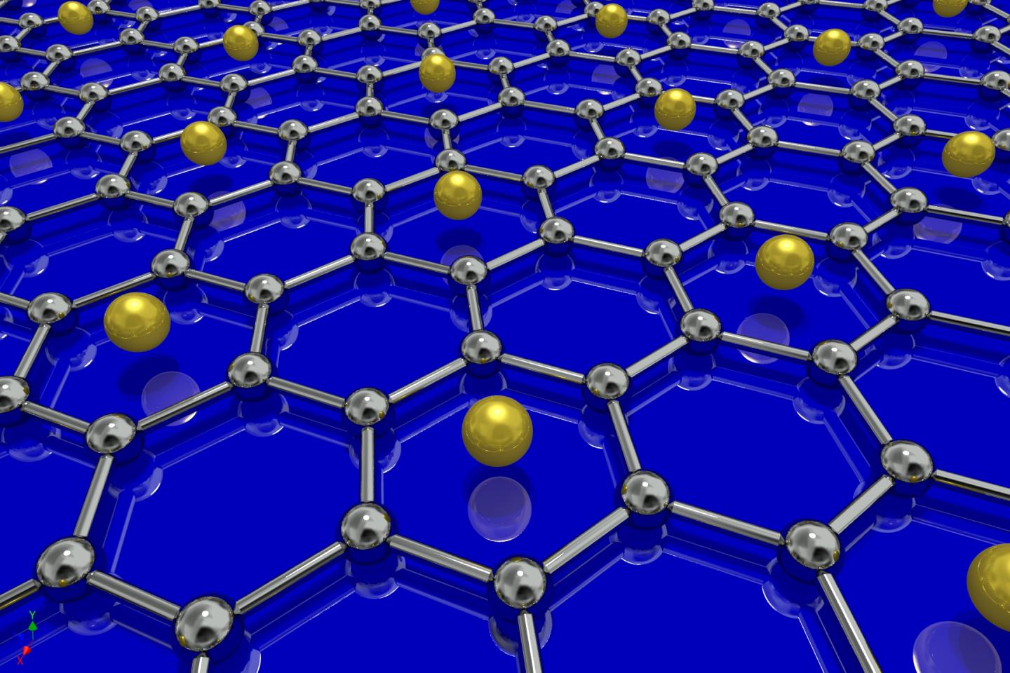
University of British Columbia physicists have created the first superconducting graphene sample by coating it with lithium atoms (yellow), shown in this illustration (credit: University of British Columbia)

University of British Columbia (UBC) physicists have created the first single-layer superconducting graphene sample by coating it with lithium atoms.

Although superconductivity has already been observed in layered bulk graphite, inducing superconductivity in single-layer graphene has until now eluded scientists.

“This first experimental realization of superconductivity in graphene promises to usher us in a new era of graphene electronics and nanoscale quantum devices,” says Andrea Damascelli, director of UBC’s Quantum Matter Institute and leading scientist of the Proceedings of the National Academy of Sciences study outlining the discovery. A superconductive wire would have zero resistance at ultra-low temperatures (at a critical temperature* of about 5.9K), so a current flowing through it would generate no heat.

Given the massive scientific and technological interest, the ability to induce superconductivity in single-layer graphene promises to have significant cross-disciplinary impacts, the researchers say.

To achieve this breakthrough, the researchers, which include colleagues at the Max Planck Institute for Solid State Research, prepared the lithium-decorated graphene in ultra-high vacuum conditions.

Scientists eventually hope to make very fast transistors, semiconductors, sensors, and transparent electrodes using graphene, a single layer of carbon atoms arranged in a honeycomb pattern.

* The temperature below which superconductivity appears.

UPDATE Sept. 14, 2015: critical temperature added.


Abstract of Evidence for superconductivity in Li-decorated monolayer graphene

Monolayer graphene exhibits many spectacular electronic properties, with superconductivity being arguably the most notable exception. It was theoretically proposed that superconductivity might be induced by enhancing the electron–phonon coupling through the decoration of graphene with an alkali adatom superlattice [Profeta G, Calandra M, Mauri F (2012) Nat Phys 8(2):131–134]. Although experiments have shown an adatom-induced enhancement of the electron–phonon coupling, superconductivity has never been observed. Using angle-resolved photoemission spectroscopy (ARPES), we show that lithium deposited on graphene at low temperature strongly modifies the phonon density of states, leading to an enhancement of the electron–phonon coupling of up to λ≃0.58. On part of the graphene-derived π∗-band Fermi surface, we then observe the opening of a Δ≃0.9-meV temperature-dependent pairing gap. This result suggests for the first time, to our knowledge, that Li-decorated monolayer graphene is indeed superconducting, with Tc≃5.9 K.

Functional carbon nanotube integrated circuits: a breakthrough

Atomic force micrograph of complementary single-wall carbon nanotubes in thin-film-transistor channel (credit: Michael L. Geier et al./Nature Nanotechnology)

Northwestern University engineers say that have finally found the key to practical use of carbon nanotubes (CNTs) in integrated circuits. Individual transistors made from CNTs are faster and more energy-efficient and reliable than those made from other materials.

The problem. But making the leap to wafer-scale integrated circuits (a microprocessor typically has a billion transistors) is a challenge. The process is incredibly expensive, often requiring billion-dollar cleanrooms to keep the delicate nano-sized components safe from the potentially damaging effects of air, water, and dust.

And researchers have struggled to create a carbon nanotube-based integrated circuit in which the transistors are spatially uniform across the material, which is needed for the overall system to work.

The solution. Now Hersam and his team have found a key to solving all these issues: newly developed encapsulation layers that protect carbon nanotubes from environmental degradation.

Dealing with environmental degradation

“One of the realities of a nanomaterial, such as a carbon nanotube, is that essentially all of its atoms are on the surface,” explained Northwestern Engineering’s Mark Hersam, the Walter P. Murphy Professor of Materials Science and Engineering. “So anything that touches the surface of these materials can influence their properties.

“If we made a series of transistors and left them out in the air, water and oxygen would stick to the surface of the nanotubes, degrading them over time. We thought that adding a protective encapsulation layer could arrest this degradation process to achieve substantially longer lifetimes.”*

To demonstrate proof of concept, Hersam developed nanotube-based static random-access memory (SRAM) circuits. SRAM is a key component of all microprocessors, often making up as much as 85 percent of the transistors in the central-processing unit in a common computer. To create the encapsulated carbon nanotubes, the team first deposited the carbon nanotubes from a solution previously developed in Hersam’s lab. Then they coated the tubes with their encapsulation layers.

Functional CNT-based SRAM memory circuits

Complementary single-wall carbon nanotube thin-film-transistor (SWCNT TFT) structures. (A) Optical micrographs of the fabricated device with channel width of 150 μm and length of 50 μm (inset) and an array of SWCNT TFTs (scale bar: 1 mm). (B) Schematic cross-section of a SWCNT TFT. (C) Atomic force micrograph of the SWCNTs in the TFT channel with a linear density of ~10 SWCNTs/μm (Height color bar: 0 to 15 nm). (credit: Michael L. Geier et al./Nature Nanotechnology)

Using the encapsulated carbon nanotubes, Hersam’s team successfully designed and fabricated arrays of working SRAM circuits. Not only did the encapsulation layers protect the sensitive device from the environment, but they improved spatial uniformity among individual transistors across the wafer. While Hersam’s integrated circuits demonstrated a long lifetime, transistors that were deposited from the same solution but not coated degraded within hours.

“After we’ve made the devices, we can leave them out in air with no further precautions,” Hersam said. “We don’t need to put them in a vacuum chamber or controlled environment. Other researchers have made similar devices but immediately had to put them in a vacuum chamber or inert environment to keep them stable. That’s obviously not going to work in a real-world situation.”

Implications for portable/wearable electronics

These features, when combined with recent advances in flexible and printed electronics have potentially wide-ranging implications for high-performance portable and wearable electronics, the researchers suggest in the paper.

Flexible carbon nanotube-based transistors could replace rigid silicon to enable wearable electronics, Hersam says. The cheaper manufacturing method also opens doors for smart cards — credit cards embedded with personal information to reduce the likelihood of fraud.

“Smart cards are only realistic if they can be realized using extremely low-cost manufacturing,” he said. “Because our solution-processed carbon nanotubes are compatible with scalable and inexpensive printing methods, our results could enable smart cards and related printed electronics applications.”

The research appeared online in Nature Nanotechology on September 7. It was supported by the Office of Naval Research and the National Science Foundation.

* Hersam compares his solution to one currently used for organic light-emitting diodes (LEDs), which experienced similar problems after they were first realized. Many people assumed that organic LEDs would have no future because they degraded in air. After researchers developed an encapsulation layer for the material, organic LEDs are now used in many commercial applications, including displays for smartphones, car radios, televisions, and digital cameras. Made from polymers and inorganic oxides, Hersam’s encapsulation layer is based on the same idea but tailored for carbon nanotubes.


Abstract of Solution-processed carbon nanotube thin-film complementary static random access memory

Over the past two decades, extensive research on single-walled carbon nanotubes (SWCNTs) has elucidated their many extraordinary properties, making them one of the most promising candidates for solution-processable, high-performance integrated circuits. In particular, advances in the enrichment of high-purity semiconducting SWCNTs have enabled recent circuit demonstrations including synchronous digital logic, flexible electronics and high-frequency applications. However, due to the stringent requirements of the transistors used in complementary metal–oxide–semiconductor (CMOS) logic as well as the absence of sufficiently stable and spatially homogeneous SWCNT thin-film transistors, the development of large-scale SWCNT CMOS integrated circuits has been limited in both complexity and functionality. Here, we demonstrate the stable and uniform electronic performance of complementary p-type and n-type SWCNT thin-film transistors by controlling adsorbed atmospheric dopants and incorporating robust encapsulation layers. Based on these complementary SWCNT thin-film transistors, we simulate, design and fabricate arrays of low-power static random access memory circuits, achieving large-scale integration for the first time based on solution-processed semiconductors.

An experimental ultrafast optical transistor based on a silicon nanoparticle

An illustration of a silicon nanoparticle switching between modes, depending on the intensity of a laser pulse (credit: Nano Letters)

Russian physicists have invented an optical version of a transistor, based on a silicon nanoparticle. The research could lead to optical computers in the future.

Current computers are limited by the time needed to trigger a transistor — usually around 0.1 to 1 nanosecond (10−9 of a second). An optical transistor could work up to 1000 times faster — at picoseconds (10−12 of a second), the researchers explain.

In the study, a group of Russian scientists from ITMO University, Lebedev Physical Institute and Academic University in Saint Petersburg created a new approach to designing optical transistors, based on a prototype using only one silicon nanoparticle.

They achieved this by irradiating the silicon nanoparticle with an intense, ultrashort laser pulse*, which caused the nanoparticle to switch the direction in which incident light was scattered. The next step is to introduce introduce a signal beam.

The study was published in the scientific journal Nano Letters.

* The laser acts as a control beam, providing ultrafast photoexcitation of dense and rapidly recombining electron-hole plasma whose presence changes the dielectric permittivity of silicon for a few picoseconds. This abrupt change in the optical properties of the nanoparticle allowed for controlling the direction in which incident light was scattered.


Abstract of Tuning of Magnetic Optical Response in a Dielectric Nanoparticle by Ultrafast Photoexcitation of Dense Electron–Hole Plasma

We propose a novel approach for efficient tuning of optical properties of a high refractive index subwavelength nanoparticle with a magnetic Mie-type resonance by means of femtosecond laser irradiation. This concept is based on ultrafast photoinjection of dense (>1020 cm–3) electron–hole plasma within such nanoparticle, drastically changing its transient dielectric permittivity. This allows manipulation by both electric and magnetic nanoparticle responses, resulting in dramatic changes of its scattering diagram and scattering cross section. We experimentally demonstrate 20% tuning of reflectance of a single silicon nanoparticle by femtosecond laser pulses with wavelength in the vicinity of the magnetic dipole resonance. Such a single-particle nanodevice enables designing of fast and ultracompact optical switchers and modulators.

New laser design could dramatically shrink autonomous-vehicle 3-D laser-ranging systems

This self-sweeping laser couples an optical field with the mechanical motion of a high-contrast grating (HCG) mirror. The HCG mirror is supported by mechanical springs connected to layers of semiconductor material. The red layer represents the laser’s gain (for light amplification), and the blue layers form the system’s second mirror. The force of the light causes the top mirror to vibrate at high speed. The vibration allows the laser to automatically change color as it scans. (credit: Weijian Yang)

UC Berkeley engineers have invented a new laser-ranging system that can reduce the power consumption, size, weight and cost of LIDAR (light detection and ranging, aka “light radar”), which is used in self-driving vehicles* to determine the distance to an object, and in real-time image capture for 3D videos.

“The advance could shrink components that now take up the space of a shoebox down to something compact and lightweight enough for smartphones or small UAVs [unmanned aerial vehicles],” said Connie Chang-Hasnain, a professor of electrical engineering and computer sciences at UC Berkeley.

Google self-driving cars use LIDAR (shown on top) to determine the distance of objects around them (credit: Google)

A system called optical coherence tomography (OCT) used in 3D medical imaging (especially for the retina) would also benefit.

A minaturized 3-D laser-mirror system

A team used a novel concept to automate the way a light source changes its wavelength as it sweeps the surrounding landscape, as reported in an open-access paper in the journal Scientific Reports, published Thursday, Sept. 3.

In both applications, as the laser moves along, it must continuously change its frequency so that it can calculate the difference between the incoming, reflected light and the outgoing light. To change the frequency, at least one of the two mirrors in the laser cavity must move precisely.

“The mechanisms needed to control the mirrors are a part of what makes current LIDAR and OCT systems bulky, power-hungry, slow and complex,” study lead author Weijian Yang explained. “The faster the system must perform — such as in self-driving vehicles that must avoid collisions — the more power it needs.”

The novelty of the new design is that they have integrated the semiconductor laser with the mirror. That means a laser can be as small as a few hundred micrometers square, powered by an AA battery.

The study authors said the next stage of the research will be to incorporate this new laser design in current LIDAR or OCT systems and demonstrate its application in 3-D video imaging.

A U.S. Department of Defense National Security Science and Engineering Faculty Fellowship helped support this work.

* Google’s robotic cars have about $150,000 in equipment including a $70,000 LIDAR system. The range finder mounted on the top is a Velodyne 64-beam laser. This laser allows the vehicle to generate a detailed 3D map of its environment. The car then takes these generated maps and combines them with high-resolution maps of the world, producing different types of data models that allow it to drive itself. — “Google driverless car,” Wikipedia


Abstract of Laser optomechanics

Cavity optomechanics explores the interaction between optical field and mechanical motion. So far, this interaction has relied on the detuning between a passive optical resonator and an external pump laser. Here, we report a new scheme with mutual coupling between a mechanical oscillator supporting the mirror of a laser and the optical field generated by the laser itself. The optically active cavity greatly enhances the light-matter energy transfer. In this work, we use an electrically-pumped vertical-cavity surface-emitting laser (VCSEL) with an ultra-light-weight (130 pg) high-contrast-grating (HCG) mirror, whose reflectivity spectrum is designed to facilitate strong optomechanical coupling, to demonstrate optomechanically-induced regenerative oscillation of the laser optomechanical cavity. We observe >550 nm self-oscillation amplitude of the micromechanical oscillator, two to three orders of magnitude larger than typical, and correspondingly a 23 nm laser wavelength sweep. In addition to its immediate applications as a high-speed wavelength-swept source, this scheme also offers a new approach for integrated on-chip sensors.