Magnetic fields provide a lower-power, more secure wireless body network

This is a prototype of the magnetic field human body communication, developed at UC San Diego, consists of magnetic-field-generating coils wrapped around three parts of the body, including the head, arm and leg (credit: Jacobs School of Engineering, UC San Diego)

A new wireless communication technique that works by sending magnetic signals through the human body could offer a lower power and more secure way to communicate information between wearable electronic devices than Bluetooth, according to electrical engineers at the University of California, San Diego.

While this work is still a proof-of-concept demonstration, researchers envision developing it into an ultra-low-power wireless system that can easily transmit information around the human body. One use would be a wireless sensor network for full-body health monitoring.

“In the future, people are going to be wearing more electronics, such as smart watches, fitness trackers and health monitors. All of these devices will need to communicate information with each other. Currently, these devices transmit information using Bluetooth radios, which use a lot of power to communicate. We’re trying to find new ways to communicate information around the human body that use much less power,” said Patrick Mercier, a professor in the Department of Electrical and Computer Engineering at UC San Diego who led the study. Mercier also serves as the co-director of the UC San Diego Center for Wearable Sensors.

Bluetooth technology uses high-frequency electromagnetic radiation to transmit data; at those frequencies, radio signals do not easily pass through the human body, so they require a power boost to help overcome this signal obstruction, or “path loss.”

Lower power consumption

In this study, electrical engineers demonstrated a technique called “magnetic field human body communication” (mHBC), which uses the body as a vehicle to deliver magnetic energy between electronic devices. An advantage of this system is that magnetic fields are able to pass freely through biological tissues, so signals are communicated with much lower path losses and potentially, much lower power consumption.

In their experiments, researchers demonstrated that the magnetic communication link works well on the body, but they did not test the technique’s power consumption. However, the showed that the path losses associated with magnetic field human body communication are upwards of 10 million times lower than those associated with Bluetooth radios.

“This technique, to our knowledge, achieves the lowest path losses out of any wireless human body communication system that’s been demonstrated so far. This technique will allow us to build much lower power wearable devices,” said Mercier.

Lower power consumption also leads to longer battery life. “A problem with wearable devices like smart watches is that they have short operating times because they are limited to using small batteries. With this magnetic field human body communication system, we hope to significantly reduce power consumption as well as how frequently users need to recharge their devices,” said Jiwoong Park, a Ph.D student in Mercier’s Energy-Efficient Microsystems Lab at the UC San Diego Jacobs School of Engineering and first author of the study.

Human body communication schemes: (a) galvanic coupling using electric fields, (b) capacitive coupling using electric fields, and (c) the proposed magnetic resonant coupling scheme (credit: Jiwoong Park and Patrick P. Mercier)

The engineers presented their findings Aug. 26 at the 37th Annual International Conference of the IEEE Engineering in Medicine and Biology Society in Milan, Italy. In a forthcoming paper, they also compare their mHBC scheme to two earlier electric field human body communication (eHBC) schemes: galvanic coupling (using electric currents) and capacitive eHBC, also known as a wireless Body Area Network (using near-field radio frequencies); both have high path loss and other problems, they note.

Better security

The researchers also pointed out that this technique does not pose any serious health risks. Since this technique is intended for applications in ultra low power communication systems, the transmitting power of the magnetic signals sent through the body is expected to be many times lower than that of MRI scanners and wireless implant devices.

Another potential advantage of magnetic field human body communication is that it could offer more security than Bluetooth networks. Because Bluetooth radio communicates data over the air, anyone standing within 30 feet can potentially eavesdrop on that communication link. On the other hand, magnetic field human body communication employs the human body as a communication medium, making the communication link less vulnerable to eavesdropping. With this technique, researchers demonstrated that magnetic communication is strong on the body but dramatically decreases off the body. To put this in the context of a personal full-body wireless communication network, information would neither be radiated off the body nor be transmitted from one person to another.

“Increased privacy is desirable when you’re using your wearable devices to transmit information about your health,” said Park.

A proof-of-concept prototype

The researchers built a prototype to demonstrate the magnetic field human body communication technique. The prototype consists of copper wires insulated with PVC tubes. On one end, the copper wires are hooked up to an external analyzer and on the other end, the wires are wrapped in coils around three areas of the body: the head, arms and legs. These coils serve as sources for magnetic fields and are able to send magnetic signals from one part of the body to another using the body as a guide. With this prototype, researchers were able to demonstrate and measure low path loss communication from arm to arm, from arm to head, and from arm to leg.

Researchers noted that a limitation of this technique is that magnetic fields require circular geometries in order to propagate through the human body. Devices like smart watches, headbands and belts will all work well using magnetic field human body communication, but not a small patch that is stuck on the chest and used to measure heart rate, for example. As long as the wearable application can wrap around a part of the body, it should work just fine with this technique, researchers explained.

UPDATE Sept. 5, 2015 — ADDED (with illustration): In a forthcoming paper, they also compare their mHBC scheme to two earlier electric field human body communication (eHBC) schemes: galvanic coupling (using electric currents) and capacitive eHBC, also known as a wireless Body Area Network (using near-field radio frequencies); both have high path loss and other problems, they note.
Light-speed interconnects may lead to ultra-high-speed computers

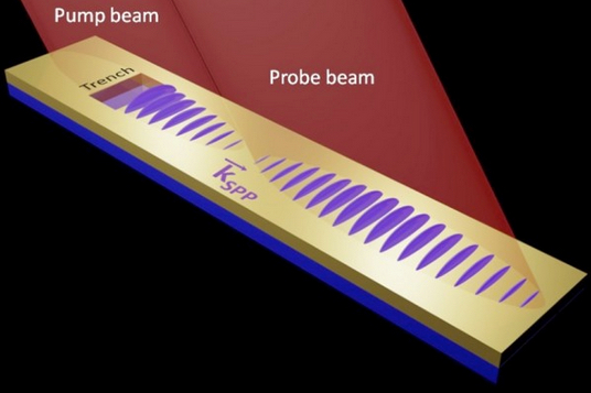
Specially designed, extremely small metal structures can trap light. Once trapped, the light becomes a confined wave known as surface plasmons. The surface plasmons are represented here by the blue waves, which begin at the pump beam and are detected 250 micrometers away by the probe beam, traveling at almost as fast as light through the air. (credit: Hess et al./Nano Lett.)

Light waves trapped on a metal’s surface (surface plasmons) travel farther than expected, up to 250 micrometers from the source — which may be far enough to create ultra-fast nanoelectronic circuits, researchers at Pacific Northwest National Laboratory have discovered.

Future computer circuits could use this phenomenon as interconnects between nanocircuits. Because a surface plasmon travels at near the speed of light, computer circuits with this technology could operate at much faster speeds than current electronics, which use copper wires.

In their experiments, the team applied two laser pulses to a gold sample surface: the first laser pulse, the “pump,” generates the surface plasmon; the second pulse, the “probe,” detects the surface plasmon after a short time delay.

By continuously tuning the time delay between the pump and probe pulses, the team monitored the motion of the plasmon on the gold surface. They captured the confined waves propagating on video, helping to directly extract details such as wavelength and speed. They also determined that a propagating plasmon can be detected at least 250 micrometers (millionths of a meter) away from the generation source — far enough to be useful in electronic circuits.

This finding may lead to ultra-fast computers and devices in the biological, health, and energy arenas.


Abstract of Ultrafast Imaging of Surface Plasmons Propagating on a Gold Surface

We record time-resolved nonlinear photoemission electron microscopy (tr-PEEM) images of propagating surface plasmons (PSPs) launched from a lithographically patterned rectangular trench on a flat gold surface. Our tr-PEEM scheme involves a pair of identical, spatially separated, and interferometrically locked femtosecond laser pulses. Power-dependent PEEM images provide experimental evidence for a sequential coherent nonlinear photoemission process, in which one laser source launches a PSP through a linear interaction, and the second subsequently probes the PSP via two-photon photoemission. The recorded time-resolved movies of a PSP allow us to directly measure various properties of the surface-bound wave packet, including its carrier wavelength (783 nm) and group velocity (0.95c). In addition, tr-PEEM images reveal that the launched PSP may be detected at least 250 μm away from the coupling trench structure.

3D-printed swimming microrobots can sense and remove toxins

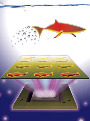
3D-printed microfish contain functional nanoparticles that enable them to be self-propelled, chemically powered and magnetically steered. The microfish are also capable of removing and sensing toxins. (credit: J. Warner, UC San Diego Jacobs School of Engineering)

A new kind of fish-shaped microrobots called “microfish” can swim around efficiently in liquids, are chemically powered by hydrogen peroxide, and magnetically controlled. They will inspire a new generation of “smart” microrobots that have diverse capabilities such as detoxification, sensing, and directed drug delivery, said nanoengineers at the University of California, San Diego.

To manufacture the microfish, the researchers used an innovative 3D printing technology they developed, with numerous improvements over other methods traditionally employed to create microrobots, such as microjet engines, microdrillers, and microrockets.

Most of these microrobots are incapable of performing more sophisticated tasks because they feature simple mechanical designs — such as spherical or cylindrical structures — and are made of homogeneous inorganic materials.

The research, led by Professors Shaochen Chen and Joseph Wang of the NanoEngineering Department at the UC San Diego, was published in the Aug. 12 issue of the journal Advanced Materials.

A microrobotic toxin scavenger

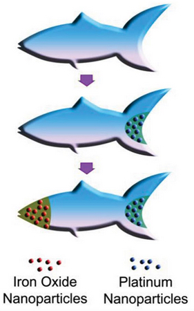
Platinum nanoparticles in the tail of the fish achieve propulsion via reaction with hydrogen peroxide; iron oxide nanoparticles are loaded into the head of the fish for magnetic control (credit: W. Zhu and J. Li, UC San Diego Jacobs School of Engineering)

The nanoengineers were able to easily add functional nanoparticles into certain parts of the microfish bodies.

They installed platinum nanoparticles in the tails, which react with hydrogen peroxide to propel the microfish forward, and magnetic iron oxide nanoparticles in the heads, which allowed them to be steered with magnets.

“We have developed an entirely new method to engineer nature-inspired microscopic swimmers that have complex geometric structures and are smaller than the width of a human hair.

With this method, we can easily integrate different functions inside these tiny robotic swimmers for a broad spectrum of applications,” said the co-first author Wei Zhu, a nanoengineering Ph.D. student in Chen’s research group at the Jacobs School of Engineering at UC San Diego.

As a proof-of-concept demonstration, the researchers incorporated toxin-neutralizing polydiacetylene (PDA) nanoparticles throughout the bodies of the microfish to neutralize harmful pore-forming toxins such as the ones found in bee venom.

The researchers noted that the powerful swimming of the microfish in solution greatly enhanced their ability to clean up toxins.

When the PDA nanoparticles bind with toxin molecules, they become fluorescent and emit red-colored light. The team was able to monitor the detoxification ability of the microfish by the intensity of their red glow. “The neat thing about this experiment is that it shows how the microfish can doubly serve as detoxification systems and as toxin sensors,” said Zhu.

“Another exciting possibility we could explore is to encapsulate medicines inside the microfish and use them for directed drug delivery,” said Jinxing Li, the other co-first author of the study and a nanoengineering Ph.D. student in Wang’s research group.

3D-printing microrobots

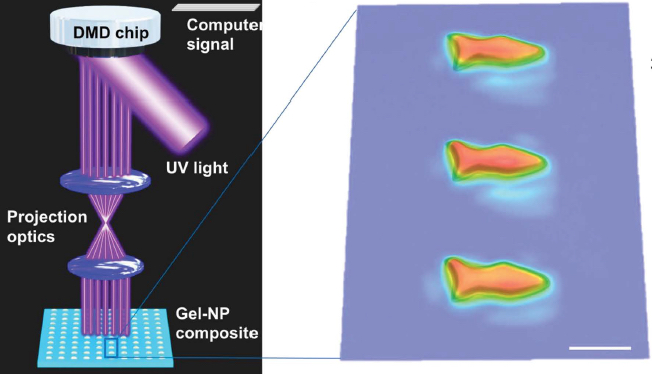
Schematic illustration of the μCOP method to fabricate microfish. (Left) UV light illuminates mirrors, generating an optical pattern specified by the control computer. The pattern is projected through optics onto the photosensitive monomer solution to fabricate the fish layer-by-layer. (Right) 3D microscopy image of an array of printed microfish. Scale bar, 100 micrometers. (credit: Wei Zhu et al./Advanced Materials)

The new microfish fabrication method is based on a rapid, high-resolution 3D printing technology called microscale continuous optical printing (μCOP) developed in Chen’s lab, offering speed, scalability, precision, and flexibility.

The key component of the μCOP technology is a digital micromirror array device (DMD) chip, which contains approximately two million micromirrors. Each micromirror is individually controlled to project UV light in the desired pattern (in this case, a fish shape) onto a photosensitive material, which solidifies upon exposure to UV light. The microfish are constructed one layer at a time, allowing each set of functional nanoparticles to be “printed” into specific parts of the fish bodies.

Fluorescent images demonstrating the detoxification capability of microfish containing encapsulated PDA nanoparticles (credit: Wei Zhu et al./Advanced Materials)

Within seconds, the researchers can print an array containing hundreds of microfish, each measuring 120 microns long and 30 microns thick. This process also does not require the use of harsh chemicals. Because the μCOP technology is digitized, the researchers could easily experiment with different designs for their microfish, including shark and manta ray shapes. They could also build microrobots in based on other biological organisms, such as birds, said Zhu.

“This method has made it easier for us to test different designs for these microrobots and to test different nanoparticles to insert new functional elements into these tiny structures. It’s my personal hope to further this research to eventually develop surgical microrobots that operate safer and with more precision,” said Li.


Abstract of 3D-Printed Artificial Microfish

Hydrogel microfish featuring biomimetic structures, locomotive capabilities, and functionalized nanoparticles are engineered using a rapid 3D printing platform: microscale continuous ­optical printing (μCOP). The 3D-printed ­microfish exhibit chemically powered and magnetically guided propulsion, as well as highly efficient detoxification capabilities that highlight the technical versatility of this platform for engineering advanced functional microswimmers for diverse biomedical applications.

Rechargeable batteries with almost infinite lifetimes coming, say MIT-Samsung engineers

Illustration of the crystal structure of a superionic conductor. The backbone of the material is a cubic-like arrangement of sulphur anions (yellow). Lithium atoms are depicted in green, PS4 tetrahedra in violet, and GeS4 tetrahedra in blue. (credit: Yan Wang)

MIT and Samsung researchers have developed a new approach to achieving long life and a 20 to 30 percent improvement in power density (the amount of power stored in a given space) in rechargeable batteries — using a solid electrolyte, rather than the liquid used in today’s most common rechargeables. The new materials could also greatly improve safety and last through “hundreds of thousands of cycles.”

The results are reported in the journal Nature Materials. Solid-state electrolytes could be “a real game-changer,” says co-author Gerbrand Ceder, MIT visiting professor of materials science and engineering, creating “almost a perfect battery, solving most of the remaining issues” in battery lifetime, safety, and cost.

Superionic lithium-ion conductors

The electrolyte in rechargeable batteries is typically a liquid organic solvent whose function is to transport charged particles from one of a battery’s two electrodes to the other during charging and discharging. That material has been responsible for the overheating and fires that, for example, resulted in a temporary grounding of all of Boeing’s 787 Dreamliner jets.

With a solid electrolyte, there’s no safety problem, he says. “You could throw it against the wall, drive a nail through it — there’s nothing there to burn.”

The key to making all this feasible, Ceder says, was finding solid materials that could conduct ions fast enough to be useful in a battery. The initial findings focused on a class of materials known as superionic lithium-ion conductors, which are compounds of lithium, germanium, phosphorus, and sulfur. But the principles derived from this research could lead to even more effective materials, the team says, and they could function below about minus 20 degrees Fahrenheit.

Researchers at the University of California at San Diego and the University of Maryland were also involved in the study.

The article title was corrected to read “infinite” instead of indefinite.


Abstract of Design principles for solid-state lithium superionic conductors

Lithium solid electrolytes can potentially address two key limitations of the organic electrolytes used in today’s lithium-ion batteries, namely, their flammability and limited electrochemical stability. However, achieving a Li+ conductivity in the solid state comparable to existing liquid electrolytes (>1 mS cm−1) is particularly challenging. In this work, we reveal a fundamental relationship between anion packing and ionic transport in fast Li-conducting materials and expose the desirable structural attributes of good Li-ion conductors. We find that an underlying body-centred cubic-like anion framework, which allows direct Li hops between adjacent tetrahedral sites, is most desirable for achieving high ionic conductivity, and that indeed this anion arrangement is present in several known fast Li-conducting materials and other fast ion conductors. These findings provide important insight towards the understanding of ionic transport in Li-ion conductors and serve as design principles for future discovery and design of improved electrolytes for Li-ion batteries.

‘Armchair nanoribbon’ design makes graphene a wafer-scalable semiconductor

Progressively zoomed-in images of graphene nanoribbons grown on germanium (gray area). The ribbons automatically align perpendicularly and naturally grow in “armchair” edge configuration. (credit: Arnold Research Group and Guisinger Research Group)

University of Wisconsin-Madison engineers have discovered a way to grow graphene nanoribbons with semiconducting properties — and directly on a conventional germanium semiconductor wafer.

Graphene, an atom-thick material with extraordinary properties, normally functions as a conductor of electricity, but not as a semiconductor. This advance is significant because it could allow manufacturers to easily use graphene nanoribbons in hybrid integrated circuits, which promise to significantly boost the performance of next-generation electronic devices.

The technology could also have specific uses in high-performance industrial and military applications, such as sensors that detect specific chemical and biological species and photonic devices that manipulate light. More importantly, the technique promises to be easily scaled up for mass production and is compatible with the prevailing fab infrastructure used in semiconductor processing.

The development was announced in an open-access paper published Aug. 10 in the journal Nature Communications by Michael Arnold, an associate professor of materials science and engineering at UW-Madison, Ph.D. student Robert Jacobberger, and their collaborators.

How to create ultra-thin “armchair” graphene nanoribbons

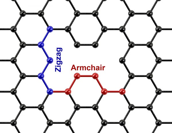
Armchair shape in graphene sheet (credit: Rajaram Narayanan/Jacobs School of Engineering/UC San Diego)

“Graphene nanoribbons that can be grown directly on the surface of a semiconductor like germanium are more compatible with planar processing that’s used in the semiconductor industry, and so there would be less of a barrier to integrating these really excellent materials into electronics in the future,” Arnold says.

Graphene, a sheet of carbon atoms that is only one atom in thickness, conducts electricity and dissipates heat much more efficiently than silicon, the material most commonly found in today’s computer chips.

But to exploit graphene’s remarkable electronic properties in semiconductor applications where current must be switched on and off, graphene nanoribbons need to be less than 10 nanometers wide. In addition, the nanoribbons must have smooth, well-defined “armchair” edges in which the carbon-carbon bonds are parallel to the length of the ribbon.

Researchers have typically fabricated nanoribbons by using lithographic techniques to cut larger sheets of graphene into ribbons. However, this “top-down” fabrication approach lacks precision and produces nanoribbons with very rough edges.

Another strategy for making nanoribbons is to use a “bottom-up” approach such as surface-assisted organic synthesis, where molecular precursors react on a surface to polymerize nanoribbons. Arnold says surface-assisted synthesis can produce beautiful nanoribbons with precise, smooth edges, but this method only works on metal substrates and the resulting nanoribbons are thus far too short for use in electronics.

Chemical vapor deposition process breakthrough

To overcome these hurdles, the UW-Madison researchers pioneered a bottom-up technique in which they grow ultra-narrow nanoribbons with smooth, straight edges directly on germanium wafers using a process called chemical vapor deposition. In this process, the researchers start with methane, which adsorbs to the germanium surface and decomposes to form various hydrocarbons. These hydrocarbons react with each other on the surface, where they form graphene.

Arnold’s team made its discovery when it explored dramatically slowing the growth rate of the graphene crystals by decreasing the amount of methane in the chemical vapor deposition chamber. They found that at a very slow growth rate, the graphene crystals naturally grow into long nanoribbons on a specific crystal facet of germanium. By simply controlling the growth rate and growth time, the researchers can easily tune the nanoribbon width be to less than 10 nanometers.

“What we’ve discovered is that when graphene grows on germanium, it naturally forms nanoribbons with these very smooth, armchair edges,” Arnold says. “The widths can be very, very narrow and the lengths of the ribbons can be very long, so all the desirable features we want in graphene nanoribbons are happening automatically with this technique.”

The nanoribbons produced with this technique start nucleating, or growing, at seemingly random spots on the germanium and are oriented in two different directions on the surface. Arnold says the team’s future work will include controlling where the ribbons start growing and aligning them all in the same direction.

The researchers are patenting their technology through the Wisconsin Alumni Research Foundation. The research was primarily supported by the Department of Energy’s Basic Energy Sciences program.


Abstract of Direct oriented growth of armchair graphene nanoribbons on germanium

Graphene can be transformed from a semimetal into a semiconductor if it is confined into nanoribbons narrower than 10 nm with controlled crystallographic orientation and well-defined armchair edges. However, the scalable synthesis of nanoribbons with this precision directly on insulating or semiconducting substrates has not been possible. Here we demonstrate the synthesis of graphene nanoribbons on Ge(001) via chemical vapour deposition. The nanoribbons are self-aligning 3° from the Geleft fence110right fence directions, are self-defining with predominantly smooth armchair edges, and have tunable width to <10 nm and aspect ratio to >70. In order to realize highly anisotropic ribbons, it is critical to operate in a regime in which the growth rate in the width direction is especially slow, <5 nm h−1. This directional and anisotropic growth enables nanoribbon fabrication directly on conventional semiconductor wafer platforms and, therefore, promises to allow the integration of nanoribbons into future hybrid integrated circuits.

A brain-computer interface for controlling an exoskeleton

A volunteer calibrating the exoskeleton brain-computer interface (credit: (c) Korea University/TU Berlin)

Scientists at Korea University and TU Berlin have developed a brain-computer interface (BCI) for a lower limb exoskeleton used for gait assistance by decoding specific signals from the user’s brain.

LEDs flickering at five different frequencies code for five different commands (credit: Korea University/TU Berlin)

Using an electroencephalogram (EEG) cap, the system allows users to move forward, turn left and right, sit, and stand, simply by staring at one of five flickering light emitting diodes (LEDs).

Each of the five LEDs flickers at a different frequency, corresponding to five types of movements. When the user focuses their attention on a specific LED, the flickering light generates a visual evoked potential in the EEG signal, which is then identified by a computer and used to control the exoskeleton to move in the appropriate manner (forward, left, right, stand, sit).


Korea University/TU Berlin | A brain-computer interface for controlling an exoskeleton

The results are published in an open-access paper today (August 18) in the Journal of Neural Engineering.

“A key problem is designing such a system is that exoskeletons create lots of electrical ‘noise,’” explains Klaus Muller, an author of the paper. “The EEG signal [from the brain] gets buried under all this noise, but our system is able to separate out the EEG signal and the frequency of the flickering LED within this signal.”

“People with amyotrophic lateral sclerosis (ALS) (motor neuron disease) or spinal cord injuries face difficulties communicating or using their limbs,” he said. This system could let them walk again, he believes. He suggests that the control system could be added on to existing BCI devices, such as Open BCI devices.

In experiments with 11 volunteers, it only took them a few minutes to be trained in operating the system. Because of the flickering LEDs, they were carefully screened for epilepsy prior to taking part in the research. The researchers are now working to reduce the “visual fatigue” associated with longer-term use.


Abstract of A lower limb exoskeleton control system based on steady state visual evoked potentials

Objective. We have developed an asynchronous brain–machine interface (BMI)-based lower limb exoskeleton control system based on steady-state visual evoked potentials (SSVEPs). 

Approach. By decoding electroencephalography signals in real-time, users are able to walk forward, turn right, turn left, sit, and stand while wearing the exoskeleton. SSVEP stimulation is implemented with a visual stimulation unit, consisting of five light emitting diodes fixed to the exoskeleton. A canonical correlation analysis (CCA) method for the extraction of frequency information associated with the SSVEP was used in combination with k-nearest neighbors.

Main results. Overall, 11 healthy subjects participated in the experiment to evaluate performance. To achieve the best classification, CCA was first calibrated in an offline experiment. In the subsequent online experiment, our results exhibit accuracies of 91.3 ± 5.73%, a response time of 3.28 ± 1.82 s, an information transfer rate of 32.9 ± 9.13 bits/min, and a completion time of 1100 ± 154.92 s for the experimental parcour studied. 

Significance. The ability to achieve such high quality BMI control indicates that an SSVEP-based lower limb exoskeleton for gait assistance is becoming feasible.

Helping Siri hear you in a party

This prototype sensor can separate out simultaneous sounds coming from different directions (credit: Steve Cummer, Duke University)

Duke University engineers have invented a device that emulates the “cocktail party effect” — the remarkable ability of the brain to home in on a single voice in a room with voices coming from multiple directions.

The device uses plastic metamaterials — the combination of natural materials in repeating patterns to achieve unnatural properties — to determine the direction of a sound and extract it from the surrounding background noise.

“We think this could improve the performance of voice-activated devices like smartphones and game consoles while also reducing the complexity of the system,” said Abel Xie, a PhD student in electrical and computer engineering at Duke and lead author of the paper.

Metamaterial and one fan-like waveguide section, showing the varying resonator cavity depths. For each person speaking, these unique cavities modify the distribution of sound strength across the frequency spectrum, creating a unique directional signature (credit: Yangbo Xie et al./PNAS)

How it works

The 3D-printed proof-of-concept plastic device looks a  pie-shaped honeycomb split into dozens of slices. The depth of resonator cavities varies within in each slice. This gives each slice of the honeycomb pie a unique sonic pattern.

“The cavities behave like soda bottles when you blow across their tops,” said Steve Cummer, professor of electrical and computer engineering at Duke. “The amount of soda left in the bottle, or the depth of the cavities in our case, affects the pitch of the sound they make, and this changes the incoming sound in a subtle but detectable way.”

When a sound wave gets to the device, it gets slightly distorted by the cavities. And that distortion has a specific signature depending what slice of the pie it passed over. After being picked up by a microphone, the sound is transmitted to a computer that separates the jumble of noises based on these unique distortions.

The researchers tested their invention in multiple trials in an anechoic chamber by simultaneously sending three identical sounds at the sensor from three different directions. It was able to distinguish between them with a 96.7 percent accuracy rate.

Uses in medical imaging, other applications

While the prototype is six inches wide, the researchers believe it could be scaled down and incorporated into the devices we use on a regular basis.

Once miniaturized, the device could have applications in voice-command electronics and medical sensing devices that use sound waves, like ultrasound imaging, said Xie. “It should also be possible to improve the sound fidelity and increase functionalities for applications like hearing aids and cochlear implants.”

The work was supported by a Multidisciplinary University Research Initiative from the Office of Naval Research. Conceivably, this design concept could be used in hydrophone-based systems to help separate out underwater sounds. It could also be used to separate out battlefield sounds and gunshots and other sounds in urban scenarios.

This research was featured in the Proceedings of the National Academy of Sciences August 11.


Abstract of Single-sensor “cocktail party listening” with acoustic metamaterials

Designing a “cocktail party listener” that functionally mimics the selective perception of a human auditory system has been pursued over the past decades. By exploiting acoustic metamaterials and compressive sensing, we present here a single-sensor listening device that separates simultaneous overlapping sounds from different sources. The device with a compact array of resonant metamaterials is demonstrated to distinguish three overlapping and independent sources with 96.67% correct audio recognition. Segregation of the audio signals is achieved using physical layer encoding without relying on source characteristics. This hardware approach to multichannel source separation can be applied to robust speech recognition and hearing aids and may be extended to other acoustic imaging and sensing applications.

MIT designs small, modular, efficient fusion power plant

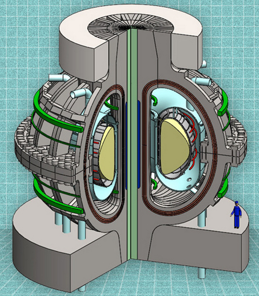
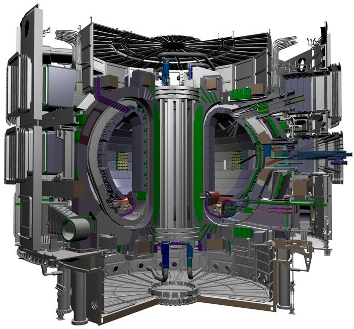
A cutaway view of the proposed ARC reactor (credit: MIT ARC team)

MIT plans to create a new compact version of a tokamak fusion reactor with the goal of producing practical fusion power, which could offer a nearly inexhaustible energy resource in as little as a decade.

Fusion, the nuclear reaction that powers the sun, involves fusing pairs of hydrogen atoms together to form helium, accompanied by enormous releases of energy.

The new fusion reactor, called ARC, would take advantage of new, commercially available superconductors — rare-earth barium copper oxide (REBCO) superconducting tapes (the dark brown areas in the illustration above) — to produce stronger magnetic field coils, according to Dennis Whyte, a professor of Nuclear Science and Engineering and director of MIT’s Plasma Science and Fusion Center.

The stronger magnetic field makes it possible to produce the required magnetic confinement of the superhot plasma — that is, the working material of a fusion reaction — but in a much smaller device than those previously envisioned. The reduction in size, in turn, makes the whole system less expensive and faster to build, and also allows for some ingenious new features in the power plant design.

The proposed reactor is described in a paper in the journal Fusion Engineering and Design, co-authored by Whyte, PhD candidate Brandon Sorbom, and 11 others at MIT.

Power plant prototype

The new reactor is designed for basic research on fusion and also as a potential prototype power plant that could produce 270MW of electrical power. The basic reactor concept and its associated elements are based on well-tested and proven principles developed over decades of research at MIT and around the world, the team says. An experimental tokamak was built at Princeton Plasma Physics Laboratory circa 1980.

The hard part has been confining the superhot plasma — an electrically charged gas — while heating it to temperatures hotter than the cores of stars. This is where the magnetic fields are so important — they effectively trap the heat and particles in the hot center of the device.

While most characteristics of a system tend to vary in proportion to changes in dimensions, the effect of changes in the magnetic field on fusion reactions is much more extreme: The achievable fusion power increases according to the fourth power of the increase in the magnetic field.

Tenfold boost in power

The new superconductors are strong enough to increase fusion power by about a factor of 10 compared to standard superconducting technology, Sorbom says. This dramatic improvement leads to a cascade of potential improvements in reactor design.

ITER — the world’s largest tokamak — is expected to be completed in 2019, with deuterium-tritium operations in 2027 and 2000–4000MW of fusion power onto the grid in 2040 (credit: ITER Organization)

The world’s most powerful planned fusion reactor, a huge device called ITER that is under construction in France, is expected to cost around $40 billion. Sorbom and the MIT team estimate that the new design, about half the diameter of ITER (which was designed before the new superconductors became available), would produce about the same power at a fraction of the cost, in a shorter construction time, and with the same physics.

Another key advance in the new design is a method for removing the fusion power core from the donut-shaped reactor without having to dismantle the entire device. That makes it especially well-suited for research aimed at further improving the system by using different materials or designs to fine-tune the performance.

In addition, as with ITER, the new superconducting magnets would enable the reactor to operate in a sustained way, producing a steady power output, unlike today’s experimental reactors that can only operate for a few seconds at a time without overheating of copper coils.

Liquid protection

Another key advantage is that most of the solid blanket materials used to surround the fusion chamber in such reactors are replaced by a liquid material that can easily be circulated and replaced, eliminating the need for costly replacement procedures as the materials degrade over time.

Right now, as designed, the reactor should be capable of producing about three times as much electricity as is needed to keep it running, but the design could probably be improved to increase that proportion to about five or six times, Sorbom says. So far, no fusion reactor has produced as much energy as it consumes, so this kind of net energy production would be a major breakthrough in fusion technology, the team says.

The design could produce a reactor that would provide electricity to about 100,000 people, they say. Devices of a similar complexity and size have been built within about five years, they say.

“Fusion energy is certain to be the most important source of electricity on earth in the 22nd century, but we need it much sooner than that to avoid catastrophic global warming,” says David Kingham, CEO of Tokamak Energy Ltd. in the UK, who was not connected with this research. “This paper shows a good way to make quicker progress,” he says.

The MIT research, Kingham says, “shows that going to higher magnetic fields, an MIT specialty, can lead to much smaller (and hence cheaper and quicker-to-build) devices.” The work is of “exceptional quality,” he says; “the next step … would be to refine the design and work out more of the engineering details, but already the work should be catching the attention of policy makers, philanthropists and private investors.”

The research was supported by the U.S. Department of Energy and the National Science Foundation.


Abstract of ARC: A compact, high-field, fusion nuclear science facility and demonstration power plant with demountable magnets

The affordable, robust, compact (ARC) reactor is the product of a conceptual design study aimed at reducing the size, cost, and complexity of a combined fusion nuclear science facility (FNSF) and demonstration fusion Pilot power plant. ARC is a ∼200–250 MWe tokamak reactor with a major radius of 3.3 m, a minor radius of 1.1 m, and an on-axis magnetic field of 9.2 T. ARC has rare earth barium copper oxide (REBCO) superconducting toroidal field coils, which have joints to enable disassembly. This allows the vacuum vessel to be replaced quickly, mitigating first wall survivability concerns, and permits a single device to test many vacuum vessel designs and divertor materials. The design point has a plasma fusion gain of Qp ≈ 13.6, yet is fully non-inductive, with a modest bootstrap fraction of only ∼63%. Thus ARC offers a high power gain with relatively large external control of the current profile. This highly attractive combination is enabled by the ∼23 T peak field on coil achievable with newly available REBCO superconductor technology. External current drive is provided by two innovative inboard RF launchers using 25 MW of lower hybrid and 13.6 MW of ion cyclotron fast wave power. The resulting efficient current drive provides a robust, steady state core plasma far from disruptive limits. ARC uses an all-liquid blanket, consisting of low pressure, slowly flowing fluorine lithium beryllium (FLiBe) molten salt. The liquid blanket is low-risk technology and provides effective neutron moderation and shielding, excellent heat removal, and a tritium breeding ratio ≥ 1.1. The large temperature range over which FLiBe is liquid permits an output blanket temperature of 900 K, single phase fluid cooling, and a high efficiency helium Brayton cycle, which allows for net electricity generation when operating ARC as a Pilot power plant.

Google Glass could bring toxicology specialists to remote emergency rooms

(credit: Google)

Researchers at the University of Massachusetts Medical School have found that Google Glass — presumably the Enterprise Edition — could effectively extend bedside toxicology consults to distant health care facilities such as community and rural hospitals to diagnose and manage poisoned patients, according to a paper in the Journal of Medical Toxicology.

“In the present era of value-based care, a toxicology service using hands-free devices, such as Google Glass, could conceivably expand its coverage area and enhance patient care, while potentially decreasing overall treatment costs,” said Peter R. Chai, MD, toxicology fellow at UMass Medical School. “Our work shows that the data transmitted by Google Glass can be used to supplement traditional telephone consults, validate bedside physical exams, and diagnose and manage patients.”

Traditional telemedicine devices usually consist of large desktop or laptop computers affixed to a big cart that has to be rolled from exam room to exam room. “Glass is positioned perfectly as an emergency medicine telemedical device. Its small, hands free and portable, so you can bring it right to the bedside and have a real-time specialist with you when you need one,” he said.

In the study, emergency medicine residents at UMass Memorial Medical Center performed 18 toxicology consults with Google Glass. ER physicians wearing Google Glass evaluated the patients at bedside while a secure video feed was sent to the toxicology supervising consultant. The supervising consultant then guided the resident through text messages displayed on the Glass. Consultants also obtained static photos of medication bottles, electrocardiograms (EKG) and other pertinent information at the discretion of the supervisor.

As a result of using Google Glass, consulting toxicologists reported being more confident in diagnosing specific toxidromes. Additional data collected showed that the use of Google Glass also changed management of patient care in more than half of the cases seen. Specifically, six of those patients received antidotes they otherwise would not have. Overall, 89 percent of the cases seen with Glass were considered successful by the consulting toxicologist.

Google currently lists several companies involved in the medical field as Glass At Work partners, such as Advanced Medical Applications, which specializes in “solutions in telemedicine, live-surgery demonstrations, and remote medical training.”

According to 9to5Google sources, the Google Glass Enterprise Edition will feature “a robust hinge mechanism that allows the computer and battery modules to fold down like a regular pair of glasses, and a hinge for folding down the left side of the band as well.” It also “includes a larger prism display for a better viewing experience, an Intel Atom processor that brings better performance, moderately improved battery life, and better heat management.”


Abstract of The Feasibility and Acceptability of Google Glass for Teletoxicology Consults

Teletoxicology offers the potential for toxicologists to assist in providing medical care at remote locations, via remote, interactive augmented audiovisual technology. This study examined the feasibility of using Google Glass, a head-mounted device that incorporates a webcam, viewing prism, and wireless connectivity, to assess the poisoned patient by a medical toxicology consult staff. Emergency medicine residents (resident toxicology consultants) rotating on the toxicology service wore Glass during bedside evaluation of poisoned patients; Glass transmitted real-time video of patients’ physical examination findings to toxicology fellows and attendings (supervisory consultants), who reviewed these findings. We evaluated the usability (e.g., quality of connectivity and video feeds) of Glass by supervisory consultants, as well as attitudes towards use of Glass. Resident toxicology consultants and supervisory consultants completed 18 consults through Glass. Toxicologists viewing the video stream found the quality of audio and visual transmission usable in 89 % of cases. Toxicologists reported their management of the patient changed after viewing the patient through Glass in 56 % of cases. Based on findings obtained through Glass, toxicologists recommended specific antidotes in six cases. Head-mounted devices like Google Glass may be effective tools for real-time teletoxicology consultation.

New solid-state memory technology allows for highest-density non-volatile storage

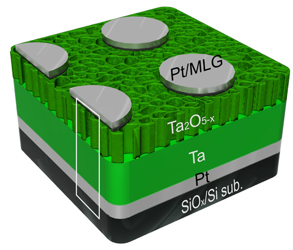
A schematic shows the layered structure of new type of solid-state memory developed at Rice University (credit: Tour Group/Rice University)

Scientists in the Rice University lab of chemist James Tour have created a solid-state memory technology that allows for high-density 162 gigabits nonvolatile storage, much higher than other oxide-based memory systems under investigation by scientists. (Eight bits equal one byte; a 162-gigabit unit would store about 20 gigabytes of information.)

Applying voltage to a 250-nanometer-thick sandwich of graphene, tantalum, nanoporous tantalum oxide (an insulator), and platinum creates addressable bits where the layers meet. Control voltages shift oxygen ions and vacancies to switch the bits between ones and zeroes.

Like the Tour lab’s previous discovery of silicon oxide memories, the new devices require only two electrodes per circuit, making them simpler than present-day flash memories, which use three. “This is a new way to make ultradense, nonvolatile computer memory,” Tour said.

Nonvolatile random-access memories, such as such as flash memory in smartphones and tablets, hold their data even when the power is off, unlike volatile random-access computer memories (in most computers), which lose their contents when the machine is shut down.

Modern memory chips have many requirements: They have to read and write data at high speed and hold as much as possible. They must also be durable and show good retention of that data while using minimal power. These are provided by Rice’s new design, which requires only one hundredth the amount of energy required with present devices, Tour says.

“This tantalum memory is based on two-terminal systems, so it’s all set for 3-D memory stacks,” he said. “And it doesn’t even need diodes or selectors, making it one of the easiest ultradense memories to construct. This will be a real competitor for the growing memory demands in high-definition video storage and server arrays.”

A layered structure of tantalum, tantalum oxide, multilayer graphene, and platinum is the basis for a new type of nonvolatile memory (credit: Tour Group/Rice University)

In making the material, the researchers found the tantalum oxide gradually loses oxygen ions, changing from an oxygen-rich, nanoporous semiconductor at the top to oxygen-poor at the bottom. Where the oxygen disappears completely, it becomes pure tantalum, a metal. The graphene does double duty as a barrier that keeps platinum from migrating into the tantalum oxide and causing a short circuit.*


Rice University | Tantalum oxide memory: Slices taken from a tantalum oxide-based memory developed at Rice University show the partially interconnected and randomly distributed internal pores in the material.

Tour said tantalum oxide memories can be fabricated at room temperature. He noted the control voltage that writes and rewrites the bits is adjustable, which allows a wide range of switching characteristics.

(As the researchers note in a paper in the journal Nano Letters, nonvolatile resistive oxide-based memories can also offer faster switching speed. That suggests that tantalum oxide memories might one day further improve MIT’s “BlueDBM” solution for improved handling of big data by making nonvolatile memory more efficient, as described on KurzweilAI last week.)

The remaining hurdles to commercialization of tantalum oxide memories include the fabrication of a dense enough crossbar device to address individual bits and a way to control the size of the nanopores.

The research is described online in the American Chemical Society Researchers at Korea University-Korea Institute of Science and Technology and University of Massachusetts, Amherst where also involved.

Tour is the T.T. and W.F. Chao Chair in Chemistry as well as a professor of materials science and nanoengineering and of computer science and a member of Rice’s Richard E. Smalley Institute for Nanoscale Science and Technology.


Rice University | Tantalum oxide memory 2

* The researchers determined three related factors give the memories their unique switching ability:

  • The control voltage mediates how electrons pass through a boundary that can flip from an ohmic (current flows in both directions) to a Schottky (current flows one way) contact and back.
  • The boundary’s location can change based on oxygen vacancies. These are “holes” in atomic arrays where oxygen ions should exist, but don’t. The voltage-controlled movement of oxygen vacancies shifts the boundary from the tantalum/tantalum oxide interface to the tantalum oxide/graphene interface. “The exchange of contact barriers causes the bipolar switching,” said Gunuk Wang, lead author of the study and a former postdoctoral researcher at Rice.
  • The flow of current draws oxygen ions from the tantalum oxide nanopores and stabilizes them. These negatively charged ions produce an electric field that effectively serves as a diode to hinder error-causing crosstalk. While researchers already knew the potential value of tantalum oxide for memories, such arrays have been limited to about a kilobyte because denser memories suffer from crosstalk that allows bits to be misread.

Abstract of Three-Dimensional Networked Nanoporous Ta2O5–x Memory System for Ultrahigh Density Storage

Oxide-based resistive memory systems have high near-term promise for use in nonvolatile memory. Here we introduce a memory system employing a three-dimensional (3D) networked nanoporous (NP) Ta2O5–x structure and graphene for ultrahigh density storage. The devices exhibit a self-embedded highly nonlinear I–V switching behavior with an extremely low leakage current (on the order of pA) and good endurance. Calculations indicated that this memory architecture could be scaled up to a ∼162 Gbit crossbar array without the need for selectors or diodes normally used in crossbar arrays. In addition, we demonstrate that the voltage point for a minimum current is systematically controlled by the applied set voltage, thereby offering a broad range of switching characteristics. The potential switching mechanism is suggested based upon the transformation from Schottky to Ohmic-like contacts, and vice versa, depending on the movement of oxygen vacancies at the interfaces induced by the voltage polarity, and the formation of oxygen ions in the pores by the electric field.