Super-elastic conducting fibers for artificial muscles, sensors, capacitors

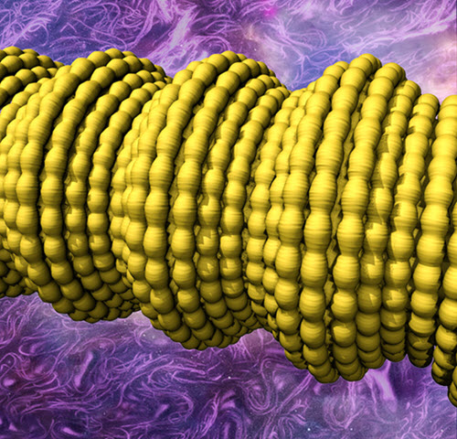
UT Dallas scientists have constructed novel fibers by wrapping sheets of tiny carbon nanotubes to form a sheath around a long rubber core. This illustration shows complex two-dimensional buckling, shown in yellow, of the carbon nanotube sheath/rubber-core fiber. The buckling results in a conductive fiber with super elasticity and novel electronic properties. (credit: UT Dallas Alan G. MacDiarmid Nanotech Institute)

An international research team based at The University of Texas at Dallas has made electrically conducting fibers that can be reversibly stretched to more than 14 times their initial length and whose electrical conductivity increases 200-fold when stretched.

The research team is using the new fibers to make artificial muscles, as well as capacitors with energy storage capacity that increases about tenfold when the fibers are stretched.

Fibers and cables derived from the invention might one day be used as interconnects for super-elastic electronic circuits, robots and exoskeletons having great reach, morphing aircraft, giant-range strain sensors, failure-free pacemaker leads, and super-stretchy charger cords for electronic devices.

Wrapping carbon nanotube sheets into fibers

In a study published in the July 24 issue of the journal Science, the scientists describe how they constructed the fibers by wrapping lighter-than-air, electrically conductive sheets of tiny carbon nanotubes to form a jelly-roll-like sheath around a long rubber core.

The new fibers differ from conventional materials in several ways. For example, when conventional fibers are stretched, the resulting increase in length and decrease in cross-sectional area restricts the flow of electrons through the material. But even a “giant” stretch of the new conducting sheath-core fibers causes little change in their electrical resistance, said Dr. Ray Baughman, senior author of the paper and director of the Alan G. MacDiarmid NanoTech Institute at UT Dallas.

One key to the performance of the new conducting elastic fibers is the introduction of buckling into the carbon nanotube sheets. Because the rubber core is stretched along its length as the sheets are being wrapped around it, when the wrapped rubber relaxes, the carbon nanofibers form a complex buckled structure, which allows for repeated stretching of the fiber.

“Think of the buckling that occurs when an accordion is compressed, which makes the inelastic material of the accordion stretchable,” said Baughman, the Robert A. Welch Distinguished Chair in Chemistry at UT Dallas.

“We make the inelastic carbon nanotube sheaths of our sheath-core fibers super stretchable by modulating large buckles with small buckles, so that the elongation of both buckle types can contribute to elasticity. These amazing fibers maintain the same electrical resistance, even when stretched by giant amounts, because electrons can travel over such a hierarchically buckled sheath as easily as they can traverse a straight sheath.”

Radical electronic and mechanical devices possible

By adding a thin overcoat of rubber to the sheath-core fibers and then another carbon nanotube sheath, the researchers made strain sensors and artificial muscles in which the buckled nanotube sheaths serve as electrodes and the thin rubber layer is a dielectric, resulting in a fiber capacitor. These fiber capacitors exhibited the unrivaled capacitance change of 860 percent when the fiber was stretched 950 percent.

Adding twist to these double-sheath fibers resulted in fast, electrically powered torsional — or rotating — artificial muscles that could be used to rotate mirrors in optical circuits or pump liquids in miniature devices used for chemical analysis. The conducting elastomers can be fabricated in diameters ranging from the very small — about 150 microns, or twice the width of a human hair — to much larger sizes, depending on the size of the rubber core. Individual small fibers also can be combined into large bundles and plied together like yarn or rope,” according to the researchers.

“This technology could be well-suited for rapid commercialization,” said Dr. Raquel Ovalle-Robles MS’06 PhD’08, an author on the paper and chief research and intellectual properties strategist at Lintec of America’s Nano-Science & Technology Center.

“The rubber cores used for these sheath-core fibers are inexpensive and readily available,” she said. “The only exotic component is the carbon nanotube aerogel sheet used for the fiber sheath.”


UT Dallas | UT Dallas Nanotech CNT rubber fiber

In this video, two lab demonstrations show the near invariance of resistance during the stretching of carbon-nanotube-sheathed rubber fibers.


UT Dallas Comets |UTD Nanotech pacemaker lead demo


Abstract of Hierarchically buckled sheath-core fibers for superelastic electronics, sensors, and muscles

Superelastic conducting fibers with improved properties and functionalities are needed for diverse applications. Here we report the fabrication of highly stretchable (up to 1320%) sheath-core conducting fibers created by wrapping carbon nanotube sheets oriented in the fiber direction on stretched rubber fiber cores. The resulting structure exhibited distinct short- and long-period sheath buckling that occurred reversibly out of phase in the axial and belt directions, enabling a resistance change of less than 5% for a 1000% stretch. By including other rubber and carbon nanotube sheath layers, we demonstrated strain sensors generating an 860% capacitance change and electrically powered torsional muscles operating reversibly by a coupled tension-to-torsion actuation mechanism. Using theory, we quantitatively explain the complementary effects of an increase in muscle length and a large positive Poisson’s ratio on torsional actuation and electronic properties.

Phosphorene could lead to ultrathin solar cells


Australian National University | Sticky tape the key to ultrathin solar cells

Scientists at Australian National University (ANU) have used simple transparent sticky (aka “Scotch”) tape to create single-atom-thick layers of phosphorene from “black phosphorus,” a black crystalline form of phosphorus similar to graphite (which is used to create graphene).

Unlike graphene, phosphorene is a natural semiconductor that can be switched on and off, like silicon, as KurzweilAI has reported. “Because phosphorene is so thin and light, it creates possibilities for making lots of interesting devices, such as LEDs or solar cells,” said lead researcher Yuerui (Larry) Lu, PhD, from ANU College of Engineering and Computer Science.

Properties that vary with layer thickness

Phosphorene is a thinner and lighter semiconductor than silicon, and it has unusual light emission properties that vary widely with the thickness of the layers, which enables more flexibility for manufacturing. “This property has never been reported before in any other material,” said Lu.

Schematic of the “puckered honeycomb” crystal structure of black phosphorus (credit: Vahid Tayari/McGill University)

“By changing the number of layers [peeled off] we can tightly control the band gap, which determines the material’s properties, such as the color of LED it would make.* “You can see quite clearly under the microscope the different colors of the sample, which tells you how many layers are there,” said Dr Lu.

The study was recently described in an open-access paper in the Nature journal Light: Science and Applications.

* Lu’s team found the optical gap for monolayer (single-layer) phosphorene was 1.75 electron volts, corresponding to red light of a wavelength of 700 nanometers. As more layers were added, the optical gap decreased. For instance, for five layers, the optical gap value was 0.8 electron volts, a infrared wavelength of 1550 nanometres. For very thick layers, the value was around 0.3 electron volts, a mid-infrared wavelength of around 3.5 microns.


Abstract of Optical tuning of exciton and trion emissions in monolayer phosphorene

Monolayer phosphorene provides a unique two-dimensional (2D) platform to investigate the fundamental dynamics of excitons and trions (charged excitons) in reduced dimensions. However, owing to its high instability, unambiguous identification of monolayer phosphorene has been elusive. Consequently, many important fundamental properties, such as exciton dynamics, remain underexplored. We report a rapid, noninvasive, and highly accurate approach based on optical interferometry to determine the layer number of phosphorene, and confirm the results with reliable photoluminescence measurements. Furthermore, we successfully probed the dynamics of excitons and trions in monolayer phosphorene by controlling the photo-carrier injection in a relatively low excitation power range. Based on our measured optical gap and the previously measured electronic energy gap, we determined the exciton binding energy to be ~0.3 eV for the monolayer phosphorene on SiO2/Si substrate, which agrees well with theoretical predictions. A huge trion binding energy of ~100 meV was first observed in monolayer phosphorene, which is around five times higher than that in transition metal dichalcogenide (TMD) monolayer semiconductor, such as MoS2. The carrier lifetime of exciton emission in monolayer phosphorene was measured to be ~220 ps, which is comparable to those in other 2D TMD semiconductors. Our results open new avenues for exploring fundamental phenomena and novel optoelectronic applications using monolayer phosphorene.

3D-printing basic electronic components

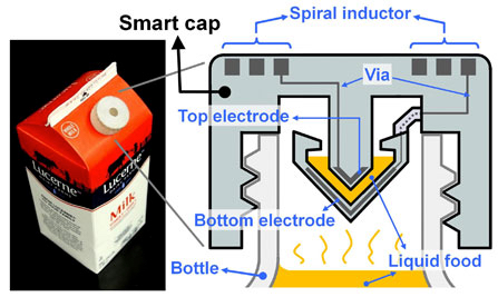
UC Berkeley engineers created a “smart cap” using 3-D-printed plastic with embedded electronics to wirelessly monitor the freshness of milk (credit: Photo and schematic by Sung-Yueh Wu)

UC Berkeley engineers, in collaboration with colleagues at Taiwan’s National Chiao Tung University, have developed a 3D printing process for creating basic electronic components, such as resistors, inductors, capacitors, and integrated wireless electrical sensing systems.

As a test, they printed a wireless “smart cap” for a milk carton that detected signs of spoilage using embedded sensors.

The findings were published Monday, July 20, in a new open-access journal in the Nature Publishing Group called Microsystems & Nanoengineering.

“Our paper describes the first demonstration of 3-D printing for working basic electrical components, as well as a working wireless sensor,” said senior author Liwei Lin, a professor of mechanical engineering and co-director of the Berkeley Sensor and Actuator Center.“One day, people may simply download 3D-printing files from the Internet with customized shapes and colors and print out useful devices at home.”

Engineers created a range of 3-D-printed electrical components, including an electrical resistor, inductor, capacitor and an LC tank (integrated inductor-capacitor system) (the penny is used for scale), shown here before removal of wax (credit: Photo by Sung-Yueh Wu)

The researchers started by printing polymers and wax. They then removed the wax, leaving hollow tubes into which liquid metal —- in their experiments they used silver — was injected and then cured.

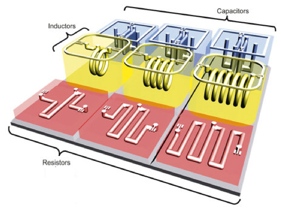
The shape and design of the metal determined the function of different electrical components. For instance, thin wires acted as resistors, and flat plates were made into capacitors.

To demonstrate their use, the researchers integrated the electronic components into a plastic milk carton cap to monitor signs of spoilage. The “smart cap” was fitted with a capacitor and an inductor to form a resonant circuit. A quick flip of the carton allowed a bit of milk to get trapped in the cap’s capacitor gap, and the entire carton was then left unopened at room temperature (about 71.6 degrees Fahrenheit) for 36 hours.

3D-printed components (credit: Sung-Yueh Wu et al./Microsystems & Nanoengineering)

The circuit could detect the changes in electrical signals that accompany increased levels of bacteria. The researchers periodically monitored the changes with a wireless radio-frequency probe at the start of the experiment and every 12 hours thereafter, up to 36 hours. The property of milk changes gradually as it degrades, leading to variations in its electrical characteristics*.

Those changes were detected wirelessly using the smart cap, which found that the peak vibration frequency of the room-temperature milk dropped by 4.3 percent after 36 hours. In comparison, a carton of milk kept in refrigeration at 39.2 degrees Fahrenheit saw a relatively minor 0.12 percent shift in frequency over the same time period.

Cheap DIY electronic circuits 

“This 3D-printing technology could eventually make electronic circuits cheap enough to be added to packaging to provide food safety alerts for consumers,” said Lin. “You could imagine a scenario where you can use your cellphone to check the freshness of food while it’s still on the store shelves.”

As 3D printers become cheaper and better, the options for electronics will expand, said Lin, though he does not think people will be printing out their own smartphones or computers anytime soon.

“That would be very difficult because of the extremely small size of modern electronics,” he said. “It might also not be practical in terms of price since current integrated circuits are made by batch fabrication to keep costs low. Instead, I see 3D-printed microelectronic devices as very promising for systems that would benefit from customization.”

Lin said his lab is working on developing this technology for health applications, such as implantable devices with embedded transducers that can monitor blood pressure, muscle strain and drug concentrations.

* As the trapped milk hardened, the dielectric constant increased, increasing the capacitance and thus decreasing the frequency.


Abstract of 3D-printed microelectronics for integrated circuitry and passive wireless sensors

Three-dimensional (3D) additive manufacturing techniques have been utilized to make 3D electrical components, such as resistors, capacitors, and inductors, as well as circuits and passive wireless sensors. Using the fused deposition modeling technology and a multiple-nozzle system with a printing resolution of 30 μm, 3D structures with both supporting and sacrificial structures are constructed. After removing the sacrificial materials, suspensions with silver particles are injected subsequently solidified to form metallic elements/interconnects. The prototype results show good characteristics of fabricated 3D microelectronics components, including an inductor–capacitor-resonant tank circuitry with a resonance frequency at 0.53 GHz. A 3D “smart cap” with an embedded inductor–capacitor tank as the wireless passive sensor was demonstrated to monitor the quality of liquid food (e.g., milk and juice) wirelessly. The result shows a 4.3% resonance frequency shift from milk stored in the room temperature environment for 36 h. This work establishes an innovative approach to construct arbitrary 3D systems with embedded electrical structures as integrated circuitry for various applications, including the demonstrated passive wireless sensors.

Korean researchers grow wafer-scale graphene on a silicon substrate

Wafer-scale (4 inch in diameter) synthesis of multi-layer graphene using high-temperature carbon ion implantation on nickel/SiO2/silicon (credit: J.Kim/Korea University, Korea)

Taking graphene a step closer to realistic commercial applications in silicon microelectronics, Korea University researchers have developed a simple microelectronics-compatible method for growing multi-layer graphene on a high-quality, wafer-scale (four inches in diameter) silicon substrate.

The method is based on the ion implantation technique — a process in which ions are accelerated under an electrical field and smashed into a semiconductor. The impacting ions change the physical, chemical, or electrical properties of the semiconductor.

Because of its high conductivity, “graphene is a potential contact electrode and an interconnection material linking semiconductor devices to form the desired electrical circuits, explained Jihyun Kim, the team leader and a professor in the Department of Chemical and Biological Engineering at Korea University.

However, “to deposit large-area graphene that is free of wrinkles, tears, and residues on silicon wafers requires low temperatures. That can’t be achieved with conventional chemical vapor deposition, which requires a high growth temperature — above 1,000 degrees Celsius.” That can cause strains, metal spiking, cracks, wrinkles, and contaminants from diffusion of dopants.

“Our synthesis method is controllable and scalable, allowing us to obtain graphene as large as the size of the silicon wafer,” Kim said. The researchers’ next step is to further lower the temperature in the synthesis process and to control the thickness of the graphene for manufacturing production.

The research is described in an open-access paper published this week in the journal Applied Physics Letters.


Abstract of Wafer-scale synthesis of multi-layer graphene by high-temperature carbon ion implantation

We report on the synthesis of wafer-scale (4 in. in diameter) high-quality multi-layer graphene using high-temperature carbon ion implantation on thin Ni films on a substrate of SiO2/Si.Carbon ions were bombarded at 20 keV and a dose of 1 × 1015 cm−2 onto the surface of the Ni/SiO2/Si substrate at a temperature of 500 °C. This was followed by high-temperature activation annealing (600–900 °C) to form a sp2-bonded honeycomb structure. The effects of post-implantation activation annealing conditions were systematically investigated by micro-Raman spectroscopy and transmission electron microscopy. Carbon ion implantation at elevated temperatures allowed a lower activation annealing temperature for fabricating large-area graphene. Our results indicate that carbon-ion implantation provides a facile and direct route for integrating graphene with Si microelectronics.

Could this new electrical brain-zap method help you learn muscle skills faster?

Three electrical brain-stimulation methods. Vertical axis: current-flow intensity; horizontal axis: time. (adapted from Shapour Jaberzadeh et al./PLOS ONE)

Researchers headed by Shapour Jaberzadeh and his group at Monash University have discovered a new noninvasive technique that could rev up your brain to improve your physical performance — for athletes and musicians, for instance — and might also improve treatments for brain-related conditions such as stroke, depression, and chronic pain.

The two neuroelectrical treatment methods currently in use are transcranial direct current simulation (tDCS) — low intensity direct current (direct current is what a battery creates) — and transcranial alternating current simulation (tACS) — current that constantly changes and reverses polarity (alternating current, or AC, is used in houses and buildings).

Introducing transcranial pulsed current stimulation

The newest method, called transcranial pulsed current stimulation (tPCS), increases more corticospinal (muscle-movement-related) excitability, according to the researchers.

“We discovered that this new treatment produced larger excitability changes in the brain,” said Jaberzadeh. In addition, increasing the length of the pulse and decreasing the [time] interval between pulses heightened excitability even further.

The research is described in a paper published Wednesday (July 15) in the open-access journal PLOS ONE.

“When we learn a task during movement training (for example playing the piano), gradually our performance gets better. This improvement coincides with enhancement of the brain excitability. Compared to tDCS, our novel technique can play an important role in enhancement of the brain excitability, which may help recipients learn new tasks faster.”

Jaberzadeh said the technique had exciting implications for a whole host of conditions in which “enhancement of the brain excitability” has a therapeutic effect. These include training for treatment of stroke and other neurological disorders, mental disorders, and even management of pain.

“Our next step is to investigate the underlying mechanisms for the efficacy of this new technique. This will enable us to develop more effective protocols for application of tPCS in patients with different pathological conditions.”

One side effect of the treatment: the patient sees lights flashing in their eyes (retinal phosphenes) — actually a plus for trippers.

New tinnitus treatment uses TMS

Transcranial magnetic stimulation being applied for tinnitus by Sarah Theodoroff, Ph.D., assistant professor of Otolaryngology/Head and Neck Surgery at OHSU (credit: VA Portland Health Care System/OHSU)

In related neuromodulation news, transcranial magnetic stimulation (TMS) significantly improved tinnitus symptoms for more than half of study participants in recent research at the VA Portland Medical Center and Oregon Health & Science University.

“For some study participants, this was the first time in years that they experienced any relief in symptoms,” according to the the researchers.

The study was funded by the Veterans Administration and published in the journal JAMA Otolaryngology — Head & Neck Surgery.

Tinnitus affects nearly 45 million Americans. People with this condition hear a persistent sound that can range from ringing or buzzing to a hissing or white noise hum when there is no external sound source. Currently, there are no proven treatments available.

Currently, the Food and Drug Administration has only approved transcranial magnetic stimulation for treatment of depression.


Abstract of Anodal Transcranial Pulsed Current Stimulation: The Effects of Pulse Duration on Corticospinal Excitability

The aim is to investigate the effects of pulse duration (PD) on the modulatory effects of transcranial pulsed current (tPCS) on corticospinal excitability (CSE). CSE of the dominant primary motor cortex (M1) of right first dorsal interosseous muscle was assessed by motor evoked potentials, before, immediately, 10, 20 and 30 minutes after application of five experimental conditions: 1) anodal transcranial direct current stimulation (a-tDCS), 2) a-tPCS with 125 ms pulse duration (a-tPCSPD = 125), 3) a-tPCS with 250 ms pulse duration (a-tPCSPD = 250), 4) a-tPCS with 500 ms pulse duration (a-tPCSPD = 500) and 5) sham a-tPCS. The total charges were kept constant in all experimental conditions except sham condition. Post-hoc comparisons indicated that a-tPCSPD = 500 produced larger CSE compared to a-tPCSPD = 125(P<0.0001), a-tPCSPD = 250 (P = 0.009) and a-tDCS (P = 0.008). Also, there was no significant difference between a-tPCSPD = 250 and a-tDCS on CSE changes (P>0.05). All conditions except a-tPCSPD = 125 showed a significant difference to the sham group (P<0.006). All participants tolerated the applied currents. It could be concluded that a-tPCS with a PD of 500ms induces largest CSE changes, however further studies are required to identify optimal values.

Abstract of Repetitive Transcranial Magnetic Stimulation Treatment for Chronic Tinnitus: A Randomized Clinical Trial

Importance Chronic tinnitus negatively affects the quality of life for millions of people. This clinical trial assesses a potential treatment for tinnitus.

Objectives To determine if repetitive transcranial magnetic stimulation (rTMS) can reduce the perception or severity of tinnitus and to test the hypothesis that rTMS will result in a statistically significantly greater percentage of responders to treatment in an active rTMS group compared with a placebo rTMS group.

Design, Setting, and Participants A randomized, participant and clinician or observer–blinded, placebo-controlled clinical trial of rTMS involving individuals who experience chronic tinnitus. Follow-up assessments were conducted at 1, 2, 4, 13, and 26 weeks after the last treatment session. The trial was conducted between April 2011 and December 2014 at Portland Veterans Affairs Medical Center among 348 individuals with chronic tinnitus who were initially screened for participation. Of those, 92 provided informed consent and underwent more detailed assessments. Seventy individuals met criteria for inclusion and were randomized to receive active or placebo rTMS. Sixty-four participants (51 men and 13 women, with a mean [SD] age of 60.6 [8.9] years) were included in the data analyses. No participants withdrew because of adverse effects of rTMS.

Interventions Participants received 2000 pulses per session of active or placebo rTMS at a rate of 1-Hz rTMS daily on 10 consecutive workdays.

Main Outcomes and Measures The Tinnitus Functional Index (TFI) was the main study outcome. Our hypothesis was tested by comparing baseline and posttreatment TFIs for each participant and group.

Results Overall, 18 of 32 participants (56%) in the active rTMS group and 7 of 32 participants (22%) in the placebo rTMS group were responders to rTMS treatment. The difference in the percentage of responders to treatment in each group was statistically significant (χ21 = 7.94, P < .005).

Conclusions and Relevance Application of 1-Hz rTMS daily for 10 consecutive workdays resulted in a statistically significantly greater percentage of responders to treatment in the active rTMS group compared with the placebo rTMS group. Improvements in tinnitus severity experienced by responders were sustained during the 26-week follow-up period. Before this procedure can be implemented clinically, larger studies should be conducted to refine treatment protocols.

Trial Registration clinicaltrials.gov Identifier: NCT01104207

Gigapixel multicolor microscope is powerful new tool to advance drug research

Parallelized multispectral imaging. Each rainbow-colored bar is the fluorescent spectrum from a discrete point in a cell culture. The gigapixel multispectral microscope records nearly a million such spectra every second. (credit: Antony Orth et al./Optica)

A new multispectral microscope capable of processing nearly 17 billion pixels in a single image has been developed by a team of researchers from the United States and Australia — the largest such microscopic image ever created.

This level of multicolor detail is essential for studying the impact of experimental drugs on biological samples and is an important advancement over traditional microscope designs, the researchers say. The goal is to simultaneously process large amounts of data to deal with a major bottleneck in pharmaceutical research: rapid, data-rich biomedical imaging.

The microscope merges data simultaneously collected by thousands of microlenses to produce a continuous series of datasets that essentially reveal how much of multiple colors (frequencies) are present at each point in a single biological sample.

“We recognized that the microscopy part of the drug development pipeline was much slower than it could be and designed a system specifically for this task,” said Antony Orth, a researcher formerly at the Rowland Institute, Harvard University in Cambridge and now with the ARC Centre for Nanoscale BioPhotonics, RMIT University in Melbourne, Australia.

Orth and his colleagues published their results in Optica, a journal of The Optical Society.

Multispectral imaging 

Multispectral imaging is used for a variety of scientific and medical research applications. This process adds data about specific colors, or frequencies to images. Medical researchers are able to study these frequencies to learn about the composition and chemical processes that are taking place within a biological sample. This is essential for pharmaceutical research — particularly cancer research — to observe how cells and tissues respond to specific chemicals and experimental drugs.

Such research, however, is very data intensive and slow since current multispectral microscopes can only survey a single point at a time with few color channels, typically only 4 or 5. This process must then be repeated over and over to scan the entire sample.

Slices of a spectral data cube. HeLa cells are imaged at 11 wavelengths from blue to red. The bottom right panel is a composite of all wavelength channels. (credit: Antony Orth et al./Optica)

Microlenses and parallel processing for big data

To overcome these limitations, Orth and his team took inspiration from modern computing, in which massive amounts of data and calculations are simultaneous handled by multicore processors. In the case of imaging, however, the work of a single microscope lens is distributed among an entire array or microlenses, each responsible for collecting multispectral data for a very narrow portion of each sample.

To capture this data, a laser is focused onto a small spot on the sample by each microlens. The laser light causes the sample to fluoresce, emitting specific wavelengths of light that differ depending on the molecules that are present. This fluorescence is then imaged back onto the camera. This is done for thousands of microlenses at once.

This multipoint scanning greatly reduces the amount of time necessary to image a sample by simultaneously harnessing thousands of lenses.

“By recording the color spectrum of the fluorescence, we can determine how much of each fluorescing molecule is in the sample,” said Orth. “What makes our microscope particularly powerful is that it records many different colors at once, allowing researchers to highlight a large number of structures in a single experiment.”

To demonstrate their design, the researchers applied various dyes that adhere to specific molecules within a cell sample. These dyes respond to laser light by fluorescing at specific frequencies so they can be detected and localized with high precision. Each microlens then looked at a very small part of the sample, an area about 0.6 by 0.1 millimeters in size. The raw data produced by this was a series of small images roughly 1,200 by 200 pixels wide.

These individual multicolor images were then stitched together into a large mosaic image. By simultaneously imaging 13 separate colors bands, the dataset produced was nearly 17 billion pixels in size.

In scientific imaging, such multilayered files are referred to as “datacubes,” because they contain three dimensions — two spatial (the X and Y coordinates) and one dimension of color. “The dataset basically tells you how much of each color you have at any given X-Y position in the sample,” explained Orth.

This design is a significant improvement over regular, single-lens microscopes, which take a series of medium-sized pictures in a serial fashion. Since they cannot see the entire sample at once, it’s necessary to take one picture and then move the sample to capture the next. This means the sample has to remain still while the microscope is refocused or color filters are changed. Orth and his colleagues’ design eliminates much of this mechanical dead-time and is almost always imaging.

Multispectral fluorescence image of an entire cancer cell culture. A gradient wavelength filter is applied in post processing to visualize the full spectral nature of the dataset – 13 discrete wavelengths from red to blue. (credit: Antony Orth et al./Optica)

Speeding up drug discovery wtih big data

This novel approach initially presented a challenge in the data pipeline. The raw data is in the form of one megapixel images recorded at 200 frames per second — a data rate much higher than current microscopes, which required the team to capture and process a tremendous amount of data each second.

Over time, the availability and prices of fast cameras and fast hard drives have come down considerably, allowing for a much more affordable and efficient design. The current limiting factor is loading the recorded data from hard drives to active computer memory to produce an image. The researchers estimate that an active memory of about 100 gigabytes to store the raw dataset would improve the entire process even further.

The goal of this technology is to speed up drug discovery. For example, to study the impact of a new cancer drug it’s essential to determine if a specific drug kills cancer cells more often than healthy cells. This requires testing the same drug on thousands to millions of cells with varying doses and under different conditions, which is normally a very time-consuming and labor-intensive task.

The new microscope presented in this paper speeds up this process while also looking at many different colors at once. “This is important because the more colors you can see, the more insightful and efficient your experiments become,” noted Orth. “Because of this, the speed-up afforded by our microscope goes beyond just the improvement in raw data rate.”

Continuing this research, the team would like to expand to live cell imaging in which billion-pixel, time-lapse movies of cells moving and responding to various stimuli could be made, opening the door to experiments that currently aren’t possible with small-scale time-lapse movies.


Abstract of Gigapixel multispectral microscopy

Understanding the complexity of cellular biology often requires capturing and processing an enormous amount of data. In high-content drug screens, each cell is labeled with several different fluorescent markers and frequently thousands to millions of cells need to be analyzed in order to characterize biology’s intrinsic variability. In this work, we demonstrate a new microlens-based multispectral microscope designed to meet this throughput-intensive demand. We report multispectral image cubes of up to 1.26 gigapixels in the spatial domain, with up to 13 spectral samples per pixel, for a total image size of 16.4 billion spatial-spectral samples. To our knowledge, this is the largest multispectral microscopy dataset reported in the literature. Our system has highly reconfigurable spectral sampling and bandwidth settings and we have demonstrated spectral unmixing of up to 6 fluorescent channels.

Why ‘white graphene’ structures are cool

A 3-D structure of hexagonal boron nitride sheets and boron nitride nanotubes could be a tunable material to control heat in electronics, according to researchers at Rice University (credit: Shahsavari Group/Rice University)


Three-dimensional structures of boron nitride are a viable candidate as a tunable material to keep electronics cool, according to scientists at Rice University researchers Rouzbeh Shahsavari and Navid Sakhavand.

Their work appears this month in the American Chemical Society journal Applied Materials and Interfaces.

In its two-dimensional form, hexagonal boron nitride (h-BN), aka white graphene, looks just like the atom-thick form of carbon known as graphene. One difference: h-BN is a natural insulator, where perfect graphene presents no barrier to electricity (is a natural electrical conductor).

But like graphene, h-BN is a also a good conductor of heat, which can be quantified in the form of phonons. (Technically, a phonon is a “quasiparticle” in a collective excitation of atoms.)

“Typically in all electronics, it is highly desired to get heat out of the system as quickly and efficiently as possible,” he said. “One of the drawbacks in electronics, especially when you have layered materials on a substrate, is that heat moves very quickly in one direction, along a conductive plane, but not so good from layer to layer. Multiple stacked graphene layers is a good example of this.”

Heat moves ballistically across flat planes of boron nitride, too, but the Rice simulations showed that 3-D structures of h-BN planes connected by boron nitride nanotubes would be able to move phonons in all directions, whether in-plane or across planes, Shahsavari said.

Phonon flows

The researchers calculated how phonons would flow across four such structures with nanotubes of various lengths and densities. They found the junctions of pillars and planes significantly slowed down the flow of phonons from layer to layer, Shahsavari said. Both the length and density of the pillars had an effect on the heat flow: more and/or shorter pillars slowed conduction, while longer pillars presented fewer barriers and thus sped things along.

Researchers have already made graphene/carbon nanotube junctions, but Shahsavari believes such junctions for boron nitride materials could be just as promising. “Given the insulating properties of boron nitride, they can enable and complement the creation of 3-D, graphene-based nanoelectronics,” Shahsavari said.

“This type of 3-D thermal-management system can open up opportunities for thermal switches, or thermal rectifiers, where the heat flowing in one direction can be different than the reverse direction. This can be done by changing the shape of the material, or changing its mass — say one side is heavier than the other — to create a switch. The heat would always prefer to go one way, but in the reverse direction it would be slower.”


Abstract of Dimensional Crossover of Thermal Transport in Hybrid Boron Nitride Nanostructures

Although Boron Nitride nanotubes (BNNT) and hexagonal-BN (h-BN) are superb one-dimensional (1D) and 2D thermal conductors respectively, bringing this quality into 3D remain elusive. Here, we focus on Pillared Boron Nitride (PBN) as a class of 3D BN allotropes and demonstrate how the junctions, pillar length and pillar distance control phonon scattering in PBN and impart tailorable thermal conductivity in 3D. Using reverse non equilibrium molecular dynamics simulations, our results indicate that while a clear phonon scattering at the junctions accounts for the lower thermal conductivity of PBN compared to its parent BNNT and h-BN allotropes, it acts as an effective design tool and provides 3D thermo-mutable features that are absent in the parent structures. Propelled by the junction spacing, while one geometrical parameter, e.g., pillar length, controls the thermal transport along the out-of-plane direction of PBN, the other parameter, e.g., pillar distance, dictates the gross cross-sectional area, which is key for design of 3D thermal management systems. Furthermore, the junctions have a more pronounced effect in creating a Kapitza effect in the out-of-plane direction, due to the change in dimensionality of the phonon transport. This work is the first report on thermo-mutable properties of hybrid BN allotropes and can potentially impact thermal management of other hybrid 3D BN architectures.

‘Smart clothes’ for personalized cooling and heating

Garment-based printable electrodes (credit: UC San Diego)

Instead of heating or cooling your whole house, imagine a fabric that will keep your body at a comfortable temperature — regardless of how hot or cold it actually is.

That’s the goal of an engineering project called ATTACH (Adaptive Textiles Technology with Active Cooling and Heating) at the University of California, San Diego, funded with a $2.6M grant from the U.S. Department of Energy’s Advanced Research Projects Agency – Energy (ARPA-E).

By regulating the temperature around an individual person, rather than a large room, the smart fabric could potentially cut the energy use of buildings and homes by at least 15 percent, said project leader Joseph Wang, distinguished professor of nanoengineering at UC San Diego.

“In cases where there are only one or two people in a large room, it’s not cost-effective to heat or cool the entire room,” said Wang. “If you can do it locally, like you can in a car by heating just the car seat instead of the entire car, you can save a lot of energy.”

Skin temperature

The smart fabric will be designed to regulate the temperature of the wearer’s skin — keeping it at 93° F — by adapting to temperature changes in the room. When the room gets cooler, the fabric will become thicker. When the room gets hotter, the fabric will become thinner, using polymers inside the smart fabric that expand in the cold and shrink in the heat.

“93° F is the average comfortable skin temperature for most people,” added Renkun Chen, assistant professor of mechanical and aerospace engineering at UC San Diego, and one of the collaborators on this project.

The clothing will incorporate printable “thermoelectrics” into specific spots of the smart fabric to regulate the temperature on “hot spots” — such as areas on the back and underneath the feet — that tend to get hotter than other parts of the body when a person is active.

Saving energy

“With the smart fabric, you won’t need to heat the room as much in the winter, and you won’t need to cool the room down as much in the summer. That means less energy is consumed,” said Chen.

The researchers are also designing the smart fabric to power itself, using rechargeable batteries to power the thermoelectrics and biofuel cells that can harvest electrical power from human sweat.

The 3-D printable wearable parts will be thin, stretchable, and flexible to ensure that the smart fabric is not bulky or heavy. The material will also be washable, stretchable, bendable and lightweight.

“We also hope to make it look attractive and fashionable to wear,” said Wang.


Using graphene-based film for efficient cooling of electronics

Graphene-based film on a hot electronic component (credit: Johan Liu)

A method for efficiently cooling electronics using graphene-based film — with a thermal conductivity capacity four times higher than copper — has been developed by researchers at Chalmers University of Technology. The film can be attached to computer chips and other silicon-based electronic components.

Electronic systems available today accumulate a great deal of heat, mostly due to the ever-increasing demand on functionality. Getting rid of excess heat in efficient ways is needed for chip lifespan and reduction in energy usage.

A research team led by Johan Liu, a professor at Chalmers University of Technology, originally found that graphene can have a cooling effect on silicon-based electronics, but that it’s not efficient because it’s limited to a few layers of graphene atoms. “When you try to add more layers of graphene, the graphene will no longer adhere to the surface, since the adhesion is [due to] weak van der Waals bonds,” he said.

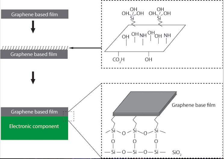
Silane coupling between graphene and silicon. After heating and hydrolysis of (3-Aminopropyl) triethoxysilane (APTES) molecules (top right), silane coupling (bottom right) is created, providing mechanical strength and good thermal pathways (credit: Johan Liu)

The researchers solved that by creating strong covalent bonds between the graphene film and the surface. The stronger bonds result from adding (3-Aminopropyl) triethoxysilane (APTES) molecules to the film. Heating and hydrolysis then creates silane bonds between the graphene and the electronic component, doubling thermal conductivity.

“Increased thermal capacity could lead to several new [cooling] applications for graphene,” says Liu, including LEDs, lasers, and radio frequency components.


Abstract of Improved Heat Spreading Performance of Functionalized Graphene in Microelectronic Device Application

It is demonstrated that a graphene-based film (GBF) functionalized with silane molecules strongly enhances thermal performance. The resistance temperature detector results show that the inclusion of silane molecules doubles the heat spreading ability. Furthermore, molecular dynamics simulations show that the thermal conductivity (κ) of the GBF increased by 15%–56% with respect to the number density of molecules compared to that with the nonfunctionalized graphene substrate. This increase in κ is attributed to the enhanced in-plane heat conduction of the GBF, resulting from the simultaneous increase of the thermal resistance between the GBF and the functionalized substrate limiting cross-plane phonon scattering. Enhancement of the thermal performance by inserting silane-functionalized molecules is important for the development of next-generation electronic devices and proposed application of GBFs for thermal management.

IBM announces first 7nm node test chips

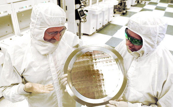
7nm node test chips (credit: Darryl Bautista/IBM)

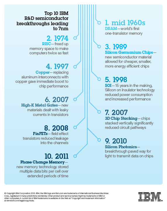
IBM Research has announced the semiconductor industry’s first 7nm (nanometer) node test chips, which could allow for chips with more than 20 billion transistors, IBM believes — a big step forward from today’s most advanced chips, made using 14nm technology.

IBM achieved the 7 nm node through a combination of new materials, tools and techniques, explained Mukesh Khare, VP, IBM Semiconductor Technology Research in a blog post. “In materials, we’re using silicon germanium for the first time in the channels on the chips that conduct electricity. We have employed a new type of lithography in the chip-making process, Extreme Ultraviolet, or EUV, which delivers order-of-magnitude improvements over today’s mainstream optical lithography.”

However, as future technology starts to hit the quantum wall, “there’s no clear path to extend the life of the silicon semiconductor further into the future,” he noted.  “The next major wave of progress, the 5 nm node, will be even more challenging than the 7 nm node has been.”

IBM 7nm node test chip closeup (credit: Darryl Bautista/IBM)

Meanwhile, industry experts consider 7nm technology crucial to meeting the anticipated demands of future cloud computing and Big Data systems, cognitive computingmobile products and other emerging technologies, says IBM. Part of IBM’s $3 billion, five-year investment in chip R&D (announced in 2014), this accomplishment was the result of a  public-private partnership with New York State and joint development alliance with GLOBALFOUNDRIES, Samsung, and equipment suppliers.

When will it be available in products? IBM “declined to speculate on when it might begin commercial manufacturing of this technology generation,” The New York Times reports. Intel’s public roadmap indicates that it’s also working on a 7 nanometer chip, Wired notes.