Using light instead of electrons promises faster, smaller, more-efficient computers and smartphones

Trapped light for optical computation (credit: Imperial College London)

By forcing light to go through a smaller gap than ever before, a research team at Imperial College London has taken a step toward computers based on light instead of electrons.

Light would be preferable for computing because it can carry much-higher-density information, it’s much faster, and more efficient (generates little to no heat). But light beams don’t easily interact with one other. So information on high-speed fiber-optic cables (provided by your cable TV company, for example) currently has to be converted (via a modem or other device) into slower signals (electrons on wires or wireless signals) to allow for processing the data on devices such as computers and smartphones.

Electron-microscope image of an optical-computing nanofocusing device that is 25 nanometers wide and 2 micrometers long, using grating couplers (vertical lines) to interface with fiber-optic cables. (credit: Nielsen et al., 2017/Imperial College London)

To overcome that limitation, the researchers used metamaterials to squeeze light into a metal channel only 25 nanometers (billionths of a meter) wide, increasing its intensity and allowing photons to interact over the range of micrometers (millionths of meters) instead of centimeters.*

That means optical computation that previously required a centimeters-size device can now be realized on the micrometer (one millionth of a meter) scale, bringing optical processing into the size range of electronic transistors.

The results were published Thursday Nov. 30, 2017 in the journal Science.

* Normally, when two light beams cross each other, the individual photons do not interact or alter each other, as two electrons do when they meet. That means a long span of material is needed to gradually accumulate the effect and make it useful. Here, a “plasmonic nanofocusing” waveguide is used, strongly confining light within a nonlinear organic polymer.


Abstract of Giant nonlinear response at a plasmonic nanofocus drives efficient four-wave mixing

Efficient optical frequency mixing typically must accumulate over large interaction lengths because nonlinear responses in natural materials are inherently weak. This limits the efficiency of mixing processes owing to the requirement of phase matching. Here, we report efficient four-wave mixing (FWM) over micrometer-scale interaction lengths at telecommunications wavelengths on silicon. We used an integrated plasmonic gap waveguide that strongly confines light within a nonlinear organic polymer. The gap waveguide intensifies light by nanofocusing it to a mode cross-section of a few tens of nanometers, thus generating a nonlinear response so strong that efficient FWM accumulates over wavelength-scale distances. This technique opens up nonlinear optics to a regime of relaxed phase matching, with the possibility of compact, broadband, and efficient frequency mixing integrated with silicon photonics.

How to open the blood-brain-barrier with precision for safer drug delivery

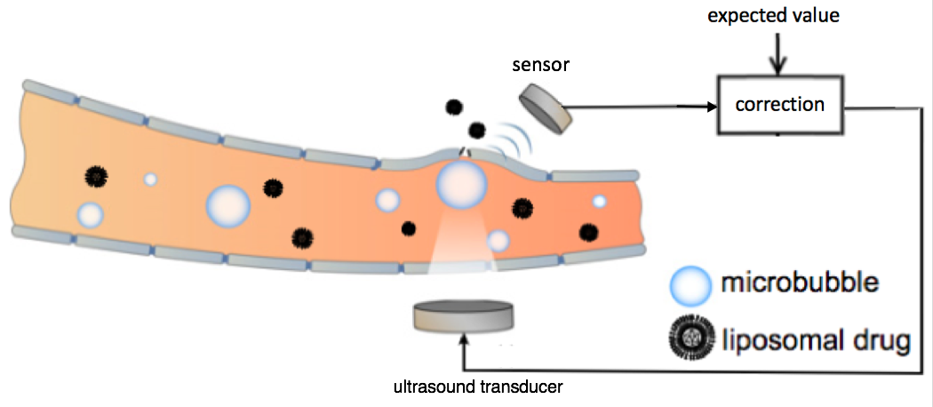
Schematic representation of the feedback-controlled focused ultrasound drug delivery system. Serving as the acoustic indicator of drug-delivery dosage, the microbubble emission signal was sensed and compared with the expected value. The difference was used as feedback to the ultrasound transducer for controlling the level of the ultrasound transmission. The ultrasound transducer and sensor were located outside the rat skull. The microbubbles were generated in the bloodstream at the target location in the brain. (credit: Tao Sun/Brigham and Women’s Hospital; adapted by KurzweilAI)

Researchers at Brigham and Women’s Hospital have developed a safer way to use focused ultrasound to temporarily open the blood-brain barrier* to allow for delivering vital drugs for treating glioma brain tumors — an alternative to invasive incision or radiation.

Focused ultrasound drug delivery to the brain uses “cavitation” — creating microbubbles — to temporarily open the blood-brain barrier. The problem with this method has been that if these bubbles destabilize and collapse, they could damage the critical vasculature in the brain.

To create a finer degree of control over the microbubbles and improve safety, the researchers placed a sensor outside of the rat brain to listen to ultrasound echoes bouncing off the microbubbles, as an indication of how stable the bubbles were.** That data was used to modify the ultrasound intensity, stabilizing the microbubbles to maintain safe ultrasound exposure.

The team tested the approach in both healthy rats and in an animal model of glioma brain cancer. Further research will be needed to adapt the technique for humans, but the approach could offer improved safety and efficacy control for human clinical trials, which are now underway in Canada.

The research, published this week in the journal Proceedings of the National Academy of Sciences, was supported by the National Institutes of Health in Canada.

* The blood brain barrier is an impassable obstacle for 98% of drugs, which it treats as pathogens and blocks them from passing from patients’ bloodstream into the brain. Using focused ultrasound, drugs can administered using an intravenous injection of innocuous lipid-coated gas microbubbles.

** For the ultrasound transducer, the researchers combined two spherically curved transducers (operating at a resonant frequency at 274.3 kHz) to double the effective aperture size and provide significantly improved focusing in the axial direction.


Abstract of Closed-loop control of targeted ultrasound drug delivery across the blood–brain/tumor barriers in a rat glioma model

Cavitation-facilitated microbubble-mediated focused ultrasound therapy is a promising method of drug delivery across the blood–brain barrier (BBB) for treating many neurological disorders. Unlike ultrasound thermal therapies, during which magnetic resonance thermometry can serve as a reliable treatment control modality, real-time control of modulated BBB disruption with undetectable vascular damage remains a challenge. Here a closed-loop cavitation controlling paradigm that sustains stable cavitation while suppressing inertial cavitation behavior was designed and validated using a dual-transducer system operating at the clinically relevant ultrasound frequency of 274.3 kHz. Tests in the normal brain and in the F98 glioma model in vivo demonstrated that this controller enables reliable and damage-free delivery of a predetermined amount of the chemotherapeutic drug (liposomal doxorubicin) into the brain. The maximum concentration level of delivered doxorubicin exceeded levels previously shown (using uncontrolled sonication) to induce tumor regression and improve survival in rat glioma. These results confirmed the ability of the controller to modulate the drug delivery dosage within a therapeutically effective range, while improving safety control. It can be readily implemented clinically and potentially applied to other cavitation-enhanced ultrasound therapies.

Consumer Technology Association inducts Ray Kurzweil, 11 other visionaries into the 2017 Consumer Technology Hall of Fame

Gary Shapiro (left) and Ray Kurzweil (right) (credit: CTA)

The Consumer Technology Association (CTA) inducted Ray Kurzweil and 11 other industry leaders into the Consumer Technology (CT) Hall of Fame at its 19th annual awards dinner, held Nov. 7, 2017 at the Rainbow Room, atop 30 Rockefeller Center in Manhattan.

CTA, formerly Consumer Electronics Association (CEA), created the Hall of Fame in 2000 to honor industry visionaries and pioneers.

A noted inventor, author, and futurist, Ray Kurzweil was the principal inventor of the first CCD flatbed scanner, the first omni-font optical character recognition, the first print-to-speech reading machine for the blind, the first text-to-speech synthesizer, the first music synthesizer capable of recreating the grand piano and other orchestral instruments, and the first commercially marketed large-vocabulary speech recognition. He has written five national best-selling books, including New York Times best sellers The Singularity Is Near (2005) and How to Create a Mind (2012).

This year’s honorees also include Mike Lazaridis, founder of BlackBerry, which created the first smartphone; Mitch Mohr, founder of Celluphone; and Charles Tandy, legendary retailer. Also honored: the team that developed the MPEG video-file-compression technique — Leonardo Chiariglione, PhD, and Hiroshi Yasuda, PhD; and the team responsible for developing a breakthrough circuit that enabled high-power sound amplification with low distortion — McIntosh Labs founder Frank McIntosh and McIntosh president Gordon Gow.

Gary Shapiro, president and CEO of CTA, praised the inductees for their contributions to the growth of the $321 billion U.S. consumer technology industry.

Kurzweil: “A bright future”

Concluding the evening, Kurzweil gave a few predictions on where he sees the industry heading: “Technology is accelerating, it’s growing exponentially. Technology is also miniaturizing. We will have devices that are as powerful as our cell phones today that are the size of blood cells in the 2030s, and they will go through our bloodstream, keeping us healthy.

“Technology has been making life better. Over the next decade with biotechnology, we will get little devices that are robotic, intelligent and can augment our immune system. I think the future is going to be dramatically better.

“Despite the progress that I’ve alluded to — there’s still a lot of human suffering — it is the advance of these exponential technologies that is going to help us overcome age-old afflictions like disease, poverty, and environmental degradation. If we keep our focus on both the promise and the peril, we’ll have a very bright future.”

With the 2017 class, the CT Hall of Fame grows to 246 inventors, engineers, retailers, journalists, and entrepreneurs who conceived, promoted, and/or wrote about the innovative technologies, products and services that connect and improve the lives of consumers around the world. The Hall of Fame inductees have been selected by a group of media and industry professionals, who judge the nominations submitted by manufacturers, retailers and industry journalists.

Complete profiles of the honorees will be included in the forthcoming November issue of It Is Innovation (i3) magazine.


New method 3D-prints fully functional electronic circuits

(Left) Conductive and polymeric inks were simultaneously inkjet-printed and solidified in a single process using UV irradiation. (Right) Microcontroller, batteries, and motors were then manually embedded in the system, creating a functioning miniature car. (credit: Ehab Saleh et al./University of Nottingham)

Researchers at the University of Nottingham have developed a method for rapidly 3D-printing fully functional electronic circuits such as antennas, medical devices, and solar-energy-collecting structures.

Unlike conventional 3D printers, these circuits can contain both both electrically conductive metallic inks (like the silver wires in the photo above) and insulating polymeric inks (like the yellow and orange support structure). A UV light is used rapidly solidify the inks).

The “multifunctional additive manufacturing” (MFAM) method combines 3D printing, which is based on layer-by-layer deposition of materials to create 3D devices, with 2D-printed electronics. It prints both conductors and insulators in a single step, expanding the range of functions in electronics (but not integrated circuits and other complex devices).

A schematic diagram showing how UV irradiation heats and solidifies conductive and dielectric inks to form the letter N  and silver tracks that connect a green LED to a power source. (credit: University of Nottingham)

The researchers discovered that silver nanoparticles in conductive inks are capable of absorbing UV light efficiently. The absorbed UV energy is converted into heat, which evaporates the solvents of the conductive ink and fuses the silver nanoparticles. This process affects only the conductive ink so it doesn’t damage any adjacent printed polymers.

For example, the method could create wristband that includes a pressure sensor, wireless communication circuitry, and capacitor (functioning as a battery), customized for the wearer — all in a single process.

The new method overcomes some of the challenges in manufacturing fully functional devices that contain plastic and metal components in complex structures, where different methods are required to solidify each material. The method speeds up the solidification process of the conductive inks to less than a minute per layer. Previously, this process took much longer to be completed using conventional heat sources such as ovens and hot plates, making it impractical when hundreds of layers are needed to form an object.


Abstract of 3D Inkjet Printing of Electronics Using UV Conversion

The production of electronic circuits and devices is limited by current manufacturing methods that limit both the form and potentially the performance of these systems. Additive manufacturing (AM) is a technology that has been shown to provide cross-sectoral manufacturing industries with significant geometrical freedom. A research domain known as multifunctional AM (MFAM) in its infancy looks to couple the positive attributes of AM with application in the electronics sector can have a significant impact on the development of new products; however, there are significant hurdles to overcome. This paper reports on the single step MFAM of 3D electronic circuitry within a polymeric structure using a combination of conductive and nonconductive materials within a single material jetting-based AM system. The basis of this breakthrough is a study of the optical absorption regions of a silver nanoparticle (AgNP) conductive ink which leads to a novel method to rapidly process and sinter AgNP inks in ambient conditions using simple UV radiation contemporaneously with UV-curing of deposited polymeric structures.

Integrated circuits printed directly onto fabric for the first time

A sample integrated circuit printed on fabric. (credit: Felice Torrisi)

Researchers at the University of Cambridge, working with colleagues in Italy and China, have incorporated washable, stretchable, and breathable integrated electronic circuits into fabric for the first time — opening up new possibilities for smart textiles and wearable textile electronic devices.

The circuits were made with cheap, safe, and environmentally friendly inks, and printed using conventional inkjet-printing techniques.

The new method directly prints graphene inks and other two-dimensional materials on fabric to produce integrated electronic circuits that are comfortable to wear and can survive up to 20 cycles in a typical washing machine. The technology opens up new applications of smart fabrics ranging from personal health to wearable computing, military garments, fashion, and wearable energy harvesting and storage.

(Left) Final step in fabrication of an inkjet-printed field effect transistor (FET) heterostructure on textile. (Right) Side-view schematic and photo. (credit for images: Tian Carey et al./Nature Communications; composite: KurzweilAI)

Based on earlier work on the formulation of graphene inks for printed electronics, the team designed new low-boiling-point inks, allowing them to be directly printed onto polyester fabric. They also found that roughness of the fabric improved the performance of the printed devices. The versatility of this process also allowed the researchers to design all-printed integrated electronic circuits combining active and passive components.

Non-toxic, flexible, low-power, scalable

Most wearable electronic devices that are currently available rely on rigid electronic components mounted on plastic, rubber or textiles. These have limited compatibility with the skin, are damaged when washed, and are uncomfortable to wear because they are not breathable.

“Other inks for printed electronics normally require toxic solvents and are not suitable to be worn, whereas our inks are both cheap, safe and environmentally friendly, and can be combined to create electronic circuits by simply printing different two-dimensional materials on the fabric,” said Felice Torrisi, PhD, of the Cambridge Graphene Centre, senior author of a paper describing the research in the open-access journal Nature Communications.

The process is scalable and according to the researchers, there are no fundamental obstacles to the technological development of wearable electronic devices — both in terms of their complexity and performance. The printed components are flexible, washable, and require low power — essential requirements for applications in wearable electronics.

The teams at the Cambridge Graphene Centre and Politecnico di Milano are also involved in the Graphene Flagship, an EC-funded, pan-European project dedicated to bringing graphene and GRM technologies to commercial applications.

The research was supported by grants from the Graphene Flagship, the European Research Council’s Synergy Grant, The Engineering and Physical Science Research Council, The Newton Trust, the International Research Fellowship of the National Natural Science Foundation of China and the Ministry of Science and Technology of China. The technology is being commercialized by Cambridge Enterprise, the University’s commercialization arm.


Abstract of Fully inkjet-printed two-dimensional material field-effect heterojunctions for wearable and textile electronics

Fully printed wearable electronics based on two-dimensional (2D) material heterojunction structures also known as heterostructures, such as field-effect transistors, require robust and reproducible printed multi-layer stacks consisting of active channel, dielectric and conductive contact layers. Solution processing of graphite and other layered materials provides low-cost inks enabling printed electronic devices, for example by inkjet printing. However, the limited quality of the 2D-material inks, the complexity of the layered arrangement, and the lack of a dielectric 2D-material ink able to operate at room temperature, under strain and after several washing cycles has impeded the fabrication of electronic devices on textile with fully printed 2D heterostructures. Here we demonstrate fully inkjet-printed 2D-material active heterostructures with graphene and hexagonal-boron nitride (h-BN) inks, and use them to fabricate all inkjet-printed flexible and washable field-effect transistors on textile, reaching a field-effect mobility of ~91 cm2 V−1 s−1, at low voltage (<5 V). This enables fully inkjet-printed electronic circuits, such as reprogrammable volatile memory cells, complementary inverters and OR logic gates.

New magnetism-control method could lead to ultrafast, energy-efficient computer memory

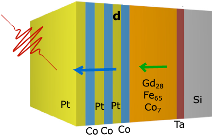
A cobalt layer on top of a gadolinium-iron alloy allows for switching memory with a single laser pulse in just 7 picoseconds. The discovery may lead to a computing processor with high-speed, non-volatile memory right on the chip. (credit: Jon Gorchon et al./Applied Physics Letters)

Researchers at UC Berkeley and UC Riverside have developed an ultrafast new method for electrically controlling magnetism in certain metals — a breakthrough that could lead to more energy-efficient computer memory and processing technologies.

“The development of a non-volatile memory that is as fast as charge-based random-access memories could dramatically improve performance and energy efficiency of computing devices,” says Berkeley electrical engineering and computer sciences (EECS) professor Jeffrey Bokor, coauthor of a paper on the research in the open-access journal Science Advances. “That motivated us to look for new ways to control magnetism in materials at much higher speeds than in today’s MRAM.”


Background: RAM vs. MRAM memory

Computers use different kinds of memory technologies to store data. Long-term memory, typically a hard disk or flash drive, needs to be dense in order to store as much data as possible but is slow. The central processing unit (CPU) — the hardware that enables computers to compute — requires fast memory to keep up with the CPU’s calculations, so the memory is only used for short-term storage of information (while operations are executed).

Random access memory (RAM) is one example of such short-term memory. Most current RAM technologies are based on charge (electron) retention, and can be written at rates of billions of bits per second (bits/nanosecond). The downside of these charge-based technologies is that they are volatile, requiring constant power or else they will lose the data.

In recent years, “spintronics” magnetic alternatives to RAM, known as Magnetic Random Access Memory (MRAM), have reached the market. The advantage of using magnets is that they retain information even when memory and CPU are powered off, allowing for energy savings. But that efficiency comes at the expense of speed, which is on the order of hundreds of picoseconds to write a single bit of information. (For comparison, silicon field-effect transistors have switching delays less than 5 picoseconds.)


The researchers found a magnetic alloy made up of gadolinium and iron that could accomplish those higher speeds — switching the direction of the magnetism with a series of electrical pulses of about 10 picoseconds (one picosecond is 1,000 times shorter than one nanosecond) — more than 10 times faster than MRAM.*

A faster version, using an energy-efficient optical pulse

In a second study, published in Applied Physics Letters, the researchers were able to further improve the performance by stacking a single-element magnetic metal such as cobalt on top of the gadolinium-iron alloy, allowing for switching with a single laser pulse in just 7 picoseconds. As a single pulse, it was also more energy-efficient. The result was a computing processor with high-speed, non-volatile memory right on the chip, functionally similar to an IBM Research “in-memory” computing architecture profiled in a recent KurzweilAI article.

“Together, these two discoveries provide a route toward ultrafast magnetic memories that enable a new generation of high-performance, low-power computing processors with high-speed, non-volatile memories right on chip,” Bokor says.

The research was supported by grants from the National Science Foundation and the U.S. Department of Energy.

* The electrical pulse temporarily increases the energy of the iron atom’s electrons, causing the magnetism in the iron and gadolinium atoms to exert torque on one another, and eventually leads to a reorientation of the metal’s magnetic poles. It’s a completely new way of using electrical currents to control magnets, according to the researchers.


Abstract of Ultrafast magnetization reversal by picosecond electrical pulses

The field of spintronics involves the study of both spin and charge transport in solid-state devices. Ultrafast magnetism involves the use of femtosecond laser pulses to manipulate magnetic order on subpicosecond time scales. We unite these phenomena by using picosecond charge current pulses to rapidly excite conduction electrons in magnetic metals. We observe deterministic, repeatable ultrafast reversal of the magnetization of a GdFeCo thin film with a single sub–10-ps electrical pulse. The magnetization reverses in ~10 ps, which is more than one order of magnitude faster than any other electrically controlled magnetic switching, and demonstrates a fundamentally new electrical switching mechanism that does not require spin-polarized currents or spin-transfer/orbit torques. The energy density required for switching is low, projecting to only 4 fJ needed to switch a (20 nm)3 cell. This discovery introduces a new field of research into ultrafast charge current–driven spintronic phenomena and devices.


Abstract of Single shot ultrafast all optical magnetization switching of ferromagnetic Co/Pt multilayers

A single femtosecond optical pulse can fully reverse the magnetization of a film within picoseconds. Such fast operation hugely increases the range of application of magnetic devices. However, so far, this type of ultrafast switching has been restricted to ferrimagnetic GdFeCo
films. In contrast, all optical switching of ferromagnetic films require multiple pulses, thereby being slower and less energy efficient. Here, we demonstrate magnetization switching induced by a single laser pulse in various ferromagnetic Co/Pt multilayers grown on GdFeCo, by exploiting
the exchange coupling between the two magnetic films. Table-top depth-sensitive time-resolved magneto-optical experiments show that the Co/Pt magnetization switches within 7 ps. This coupling approach will allow ultrafast control of a variety of magnetic films, which is critical for
applications.

Controlled by a synthetic gene circuit, self-assembling bacteria build working electronic sensors

Bacteria create a functioning 3D pressure-sensor device. A gene circuit (left) triggers the production of an engineered protein that enables pattern-forming bacteria on growth membranes (center) to assemble gold nanoparticles into a hybrid organic-inorganic dome structure whose size and shape can be controlled by altering the growth environment. In this proof-of-concept demonstration, the gold structure serves as a functioning pressure switch (right) that responds to touch. (credit: Yangxiaolu Cao et al./Nature Biotechnology)

Using a synthetic gene circuit, Duke University researchers have programmed self-assembling bacteria to build useful electronic devices — a first.

Other experiments have successfully grown materials using bacterial processes (for example, MIT engineers have coaxed bacterial cells to produce biofilms that can incorporate nonliving materials, such as gold nanoparticles and quantum dots). However, they have relied entirely on external control over where the bacteria grow and they have been limited to two dimensions.

In the new study, the researchers demonstrated the production of a composite structure by programming the cells themselves and controlling their access to nutrients, but still leaving the bacteria free to grow in three dimensions.*

As a demonstration, the bacteria were programmed to assemble into a finger-pressure sensor.

To create the pressure sensor, two identical arrays of domes were grown on a membrane (left) on two substrate surfaces. The two substrates were then sandwiched together (center) so that each dome was positioned directly above its counterpart on the other substrate. A battery was connected to the domes by copper wiring. When pressure was applied (right) to the sandwich, the domes pressed into one another, causing a deformation, resulting in an increase in conductivity, with resulting increased current (as shown the arrow in the ammeter). (credit: Yangxiaolu Cao et al./Nature Biotechnology)

Inspired by nature, but going beyond it

“This technology allows us to grow a functional device from a single cell,” said Lingchong You, the Paul Ruffin Scarborough Associate Professor of Engineering at Duke. “Fundamentally, it is no different from programming a cell to grow an entire tree.”

Nature is full of examples of life combining organic and inorganic compounds to make better materials. Mollusks grow shells consisting of calcium carbonate interlaced with a small amount of organic components, resulting in a microstructure three times tougher than calcium carbonate alone. Our own bones are a mix of organic collagen and inorganic minerals made up of various salts.

Harnessing such construction abilities in bacteria would have many advantages over current manufacturing processes. In nature, biological fabrication uses raw materials and energy very efficiently. In this synthetic system, for example, tweaking growth instructions to create different shapes and patterns could theoretically be much cheaper and faster than casting the new dies or molds needed for traditional manufacturing.

“Nature is a master of fabricating structured materials consisting of living and non-living components,” said You. “But it is extraordinarily difficult to program nature to create self-organized patterns. This work, however, is a proof-of-principle that it is not impossible.”

Self-healing materials

According to the researchers, in addition to creating circuits from bacteria, if the bacteria are kept alive, it may be possible to create materials that could heal themselves and respond to environmental changes.

“Another aspect we’re interested in pursuing is how to generate much more complex patterns,” said You. “Bacteria can create complex branching patterns, we just don’t know how to make them do that ourselves — yet.”

It’s a “very exciting work,” Timothy Lu, a synthetic biologist at MIT, who was not involved in the research, told The Register. “I think this represents a major step forward in the field of living materials.” Lu believes self-assembling materials “could create new manufacturing processes that may use less energy or be better for the environment than the ones today,” the article said. “But ‘the design rules for enabling bottoms-up assembly of novel materials are still not well understood,’ he cautioned.”

The study appeared online on October 9, 2107 in Nature Biotechnology. This study was supported by the Office of Naval Research, the National Science Foundation, the Army Research Office, the National Institutes of Health, the Swiss National Science Foundation, and a David and Lucile Packard Fellowship.

* The gene circuit is like a biological package of instructions that researchers embed into a bacterium’s DNA. The directions first tell the bacteria to produce a protein called T7 RNA polymerase (T7RNAP), which then activates its own expression in a positive feedback loop. It also produces a small molecule called AHL that can diffuse into the environment like a messenger. As the cells multiply and grow outward, the concentration of the small messenger molecule hits a critical concentration threshold, triggering the production of two more proteins called T7 lysozyme and curli. The former inhibits the production of T7RNAP while the latter acts as sort of biological Velcro, which grabs onto gold nanoparticles supplied by the researchers, forming a dome shell (the structure of the sensor). The researchers were able to alter the size and shape of the dome by controlling the properties of the porous membrane it grows on. For example, changing the size of the pores or how much the membrane repels water affects how many nutrients are passed to the cells, altering their growth pattern.


Abstract of Programmed assembly of pressure sensors using pattern-forming bacteria

Conventional methods for material fabrication often require harsh reaction conditions, have low energy efficiency, and can cause a negative impact on the environment and human health. In contrast, structured materials with well-defined physical and chemical properties emerge spontaneously in diverse biological systems. However, these natural processes are not readily programmable. By taking a synthetic-biology approach, we demonstrate here the programmable, three-dimensional (3D) material fabrication using pattern-forming bacteria growing on top of permeable membranes as the structural scaffold. We equip the bacteria with an engineered protein that enables the assembly of gold nanoparticles into a hybrid organic-inorganic dome structure. The resulting hybrid structure functions as a pressure sensor that responds to touch. We show that the response dynamics are determined by the geometry of the structure, which is programmable by the membrane properties and the extent of circuit activation. Taking advantage of this property, we demonstrate signal sensing and processing using one or multiple bacterially assembled structures. Our work provides the first demonstration of using engineered cells to generate functional hybrid materials with programmable architecture.
Fast-moving spinning magnetized nanoparticles could lead to ultra-high-speed, high-density data storage

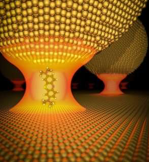
Artist’s impression of skyrmion data storage (credit: Moritz Eisebitt)

An international team led by MIT associate professor of materials science and engineering Geoffrey Beach has demonstrated a practical way to use “skyrmions” to create a radical new high-speed, high-density data-storage method that could one day replace disk drives — and even replace high-speed RAM memory.

Rather than reading and writing data one bit at a time by changing the orientation of magnetized nanoparticles on a surface, Skyrmions could store data using only a tiny area of a magnetic surface — perhaps just a few atoms across — and for long periods of time, without the need for further energy input (unlike disk drives and RAM).

Beach and associates conceive skyrmions as little sub-nanosecond spin-generating eddies of magnetism controlled by electric fields — replacing the magnetic-disk system of reading and writing data one bit at a time. In experiments, skyrmions have been generated on a thin metallic film sandwiched with non-magnetic heavy metals and transition-metal ferromagnetic layers — exploiting a defect, such as a constriction in the magnetic track.*

Skyrmions are also highly stable to external magnetic and mechanical perturbations, unlike the individual magnetic poles in a conventional magnetic storage device — allowing for vastly more data to be written onto a surface of a given size.

A practical data-storage system

Google data center (credit: Google Inc.)

Beach has recently collaborated with researchers at MIT and others in Germany** to demonstrate experimentally for the first time that it’s possible to create skyrmions in specific locations, which is needed for a data-storage system. The new findings were reported October 2, 2017 in the journal Nature Nanotechnology.

Conventional magnetic systems are now reaching speed and density limits set by the basic physics of their existing materials. The new system, once perfected, could provide a way to continue that progress toward ever-denser data storage, Beach says.

However, the researchers note that to create a commercialized system will require an efficient, reliable way to create skyrmions when and where they were needed, along with a way to read out the data (which now requires sophisticated, expensive X-ray magnetic spectroscopy). The team is now pursuing possible strategies to accomplish that.***

* The system focuses on the boundary region between atoms whose magnetic poles are pointing in one direction and those with poles pointing the other way. This boundary region can move back and forth within the magnetic material, Beach says. What he and his team found four years ago was that these boundary regions could be controlled by placing a second sheet of nonmagnetic heavy metal very close to the magnetic layer. The nonmagnetic layer can then influence the magnetic one, with electric fields in the nonmagnetic layer pushing around the magnetic domains in the magnetic layer. Skyrmions are little swirls of magnetic orientation within these layers. The key to being able to create skyrmions at will in particular locations lays in material defects. By introducing a particular kind of defect in the magnetic layer, the skyrmions become pinned to specific locations on the surface, the team found. Those surfaces with intentional defects can then be used as a controllable writing surface for data encoded in the skyrmions.

** The team also includes researchers at the Max Born Institute and the Institute of Optics and Atomic Physics, both in Berlin; the Institute for Laser Technologies in Medicine and Metrology at the University of Ulm, in Germany; and the Deutches Elektroniken-Syncrotron (DESY), in Hamburg. The work was supported by the U.S. Department of Energy and the German Science Foundation.

*** The researchers believe an alternative way of reading the data is possible, using an additional metal layer added to the other layers. By creating a particular texture on this added layer, it may be possible to detect differences in the layer’s electrical resistance depending on whether a skyrmion is present or not in the adjacent layer.


Abstract of Field-free deterministic ultrafast creation of magnetic skyrmions by spin–orbit torques

Magnetic skyrmions are stabilized by a combination of external magnetic fields, stray field energies, higher-order exchange interactions and the Dzyaloshinskii–Moriya interaction (DMI). The last favours homochiral skyrmions, whose motion is driven by spin–orbit torques and is deterministic, which makes systems with a large DMI relevant for applications. Asymmetric multilayers of non-magnetic heavy metals with strong spin–orbit interactions and transition-metal ferromagnetic layers provide a large and tunable DMI. Also, the non-magnetic heavy metal layer can inject a vertical spin current with transverse spin polarization into the ferromagnetic layer via the spin Hall effect. This leads to torques that can be used to switch the magnetization completely in out-of-plane magnetized ferromagnetic elements, but the switching is deterministic only in the presence of a symmetry-breaking in-plane field. Although spin–orbit torques led to domain nucleation in continuous films and to stochastic nucleation of skyrmions in magnetic tracks, no practical means to create individual skyrmions controllably in an integrated device design at a selected position has been reported yet. Here we demonstrate that sub-nanosecond spin–orbit torque pulses can generate single skyrmions at custom-defined positions in a magnetic racetrack deterministically using the same current path as used for the shifting operation. The effect of the DMI implies that no external in-plane magnetic fields are needed for this aim. This implementation exploits a defect, such as a constriction in the magnetic track, that can serve as a skyrmion generator. The concept is applicable to any track geometry, including three-dimensional designs.

New transistor design enables flexible, high-performance wearable/mobile electronics

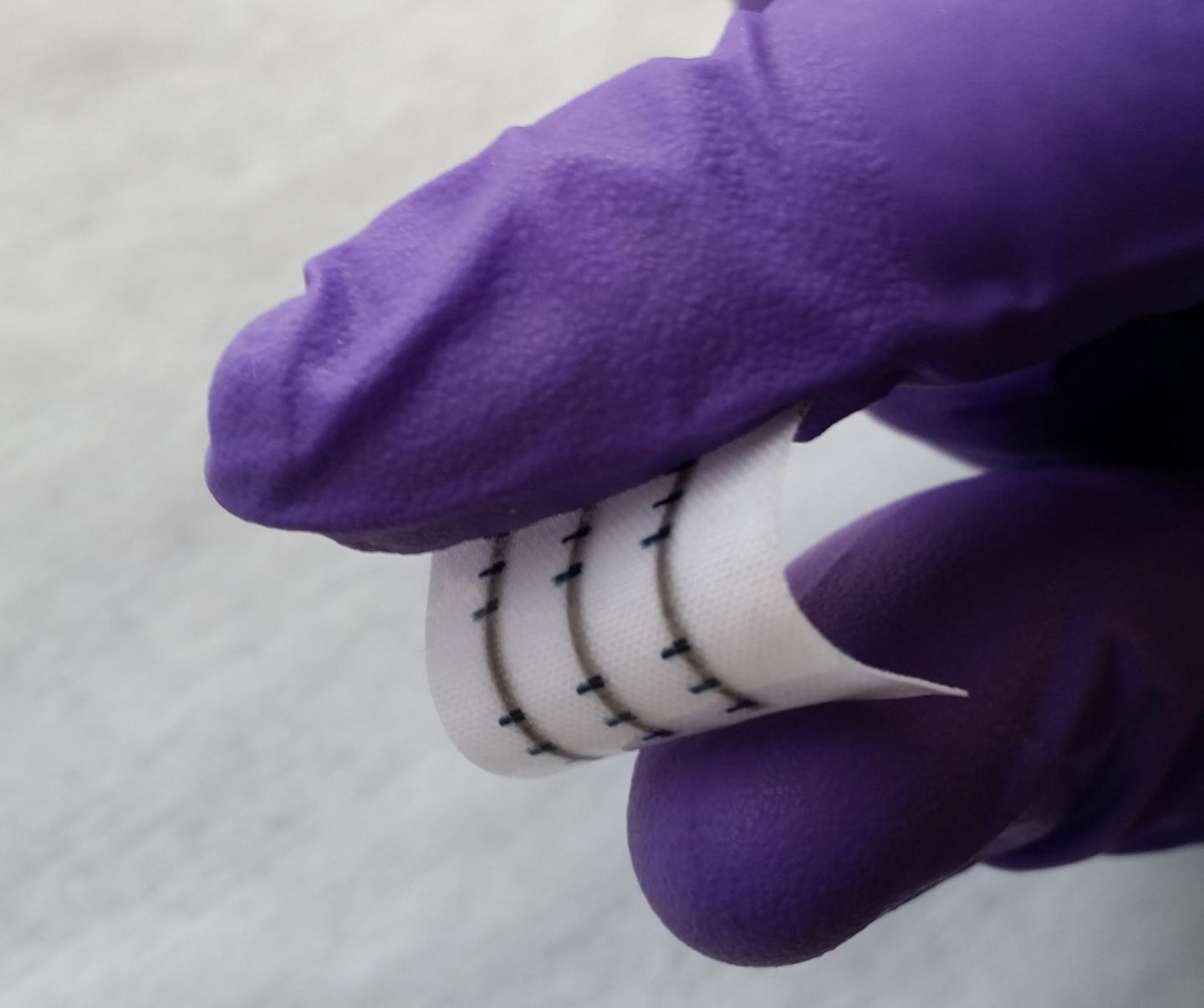
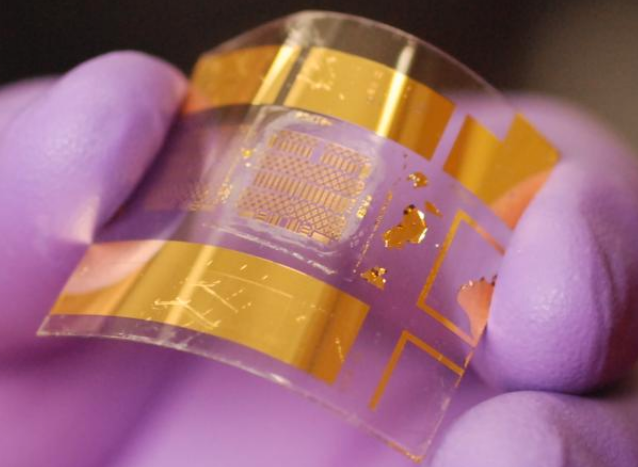
Advanced flexible transistor developed at UW-Madison (photo credit: Jung-Hun Seo/University at Buffalo, State University of New York)

A team of University of Wisconsin–Madison (UW–Madison) engineers has created “the most functional flexible transistor in the world,” along with a fast, simple, inexpensive fabrication process that’s easily scalable to the commercial level.

The development promises to allow manufacturers to add advanced, smart-wireless capabilities to wearable and mobile devices that curve, bend, stretch and move.*

The UW–Madison group’s advance is based on a BiCMOS (bipolar complementary metal oxide semiconductor) thin-film transistor, combining speed, high current, and low power dissipation (heat and wasted energy) on just one surface (a silicon nanomembrane, or “Si NM”).**

BiCMOS transistors are the chip of choice for “mixed-signal” devices (combining analog and digital capabilities), which include many of today’s portable electronic devices such as cellphones. “The [BiCMOS] industry standard is very good,” says Zhenqiang (Jack) Ma, the Lynn H. Matthias Professor and Vilas Distinguished Achievement Professor in electrical and computer engineering at UW–Madison. “Now we can do the same things with our transistor — but it can bend.”

The research was described in the inaugural issue of Nature Publishing Group’s open-access journal Flexible Electronics, published Sept. 27, 2017.***

Making traditional BiCMOS flexible electronics is difficult, in part because the process takes several months and requires a multitude of delicate, high-temperature steps. Even a minor variation in temperature at any point could ruin all of the previous steps.

Ma and his collaborators fabricated their flexible electronics on a single-crystal silicon nanomembrane on a single bendable piece of plastic. The secret to their success is their unique process, which eliminates many steps and slashes both the time and cost of fabricating the transistors.

“In industry, they need to finish these in three months,” he says. “We finished it in a week.”

He says his group’s much simpler, high-temperature process can scale to industry-level production right away.

“The key is that parameters are important,” he says. “One high-temperature step fixes everything — like glue. Now, we have more powerful mixed-signal tools. Basically, the idea is for [the flexible electronics platform] to expand with this.”

* Some companies (such as Samsung) have developed flexible displays, but not other flexible electronic components in their devices, Ma explained to KurzweilAI.

** “Flexible electronics have mainly focused on their form factors such as bendability, lightweight, and large area with low-cost processability…. To date, all the [silicon, or Si]-based thin-film transistors (TFTs) have been realized with CMOS technology because of their simple structure and process. However, as more functions are required in future flexible electronic applications (i.e., advanced bioelectronic systems or flexible wireless power applications), an integration of functional devices in one flexible substrate is needed to handle complex signals and/or various power levels.” — Jung Hun Seo et al./Flexible Electronics. The n-channel, p-channel metal-oxide semiconductor field-effect transistors (N-MOSFETs & P-MOSFETs), and NPN bipolar junction transistors (BJTs) were realized together on a 340-nm thick Si NM layer. 

*** Co-authors included researchers at the University at Buffalo, State University of New York, and the University of Texas at Arlington. This work was supported by the Air Force Office Of Scientific Research.


Abstract of High-performance flexible BiCMOS electronics based on single-crystal Si nanomembrane

In this work, we have demonstrated for the first time integrated flexible bipolar-complementary metal-oxide-semiconductor (BiCMOS) thin-film transistors (TFTs) based on a transferable single crystalline Si nanomembrane (Si NM) on a single piece of bendable plastic substrate. The n-channel, p-channel metal-oxide semiconductor field-effect transistors (N-MOSFETs & P-MOSFETs), and NPN bipolar junction transistors (BJTs) were realized together on a 340-nm thick Si NM layer with minimized processing complexity at low cost for advanced flexible electronic applications. The fabrication process was simplified by thoughtfully arranging the sequence of necessary ion implantation steps with carefully selected energies, doses and anneal conditions, and by wisely combining some costly processing steps that are otherwise separately needed for all three types of transistors. All types of TFTs demonstrated excellent DC and radio-frequency (RF) characteristics and exhibited stable transconductance and current gain under bending conditions. Overall, Si NM-based flexible BiCMOS TFTs offer great promises for high-performance and multi-functional future flexible electronics applications and is expected to provide a much larger and more versatile platform to address a broader range of applications. Moreover, the flexible BiCMOS process proposed and demonstrated here is compatible with commercial microfabrication technology, making its adaptation to future commercial use straightforward.

Artificial ‘skin’ gives robotic hand a sense of touch

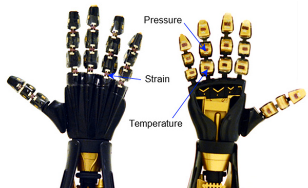
University of Houston researchers have reported a development in stretchable electronics that can serve as artificial skin for a robotic hand and biomedical devices (credit: University of Houston)

A team of researchers from the University of Houston has reported a development in stretchable electronics that can serve as an artificial skin, allowing a robotic hand to sense the difference between hot and cold, and also offering advantages for a wide range of biomedical devices.

The work, reported in the open-access journal Science Advances, describes a new mechanism for producing stretchable electronics, a process that relies upon readily available materials and could be scaled up for commercial production.

Cunjiang Yu, Bill D. Cook Assistant Professor of mechanical engineering and lead author of the paper, said the work is the first to create a semiconductor in a rubber composite format, designed to allow the electronic components to retain functionality even after the material is stretched by 50 percent.

He noted that traditional semiconductors are brittle and using them in otherwise stretchable materials has required a complicated system of mechanical accommodations. That’s both more complex and less stable than the new discovery, as well as more expensive, he said. “Our strategy has advantages for simple fabrication, scalable manufacturing, high-density integration, large strain tolerance, and low cost,” he said.

Photograph of a robotic hand with intrinsically stretchable rubbery sensors (credit: Hae-Jin Kim et al./Science Advances)

The team used the skin to demonstrate that a robotic hand could sense the temperature of hot and iced water in a cup. The skin also was able to interpret computer signals sent to the hand and reproduce the signals as American Sign Language.

Uses of the stretchable skin include soft wearable electronics such as health monitors, medical implants, and human-machine interfaces.

The stretchable composite semiconductor was prepared by using a silicon-based polymer known as polydimethylsiloxane (PDMS) and tiny nanowires to create a solution that was then hardened into a material that used the nanowires to transport electric current.


Abstract of Rubbery electronics and sensors from intrinsically stretchable elastomeric composites of semiconductors and conductors

A general strategy to impart mechanical stretchability to stretchable electronics involves engineering materials into special architectures to accommodate or eliminate the mechanical strain in nonstretchable electronic materials while stretched. We introduce an all solution–processed type of electronics and sensors that are rubbery and intrinsically stretchable as an outcome from all the elastomeric materials in percolated composite formats with P3HT-NFs [poly(3-hexylthiophene-2,5-diyl) nanofibrils] and AuNP-AgNW (Au nanoparticles with conformally coated silver nanowires) in PDMS (polydimethylsiloxane). The fabricated thin-film transistors retain their electrical performances by more than 55% upon 50% stretching and exhibit one of the highest P3HT-based field-effect mobilities of 1.4 cm2/V∙s, owing to crystallinity improvement. Rubbery sensors, which include strain, pressure, and temperature sensors, show reliable sensing capabilities and are exploited as smart skins that enable gesture translation for sign language alphabet and haptic sensing for robotics to illustrate one of the applications of the sensors.