A graphene microphone and loudspeaker that operate at up to 500 kilohertz

Construction of graphene electrostatic wideband receiver (microphone). The graphene membrane is suspended across the supporting frame (A). The membrane is electrically contacted with gold wires, and spacers are added (B) to control the distance from the membrane to the gold-coated stationary electrodes (C). (credit: Qin Zhou et al./PNAS)

University of California, Berkeley, physicists have used graphene to build lightweight ultrasonic loudspeakers and microphones, enabling people to mimic bats or dolphins’ ability to use sound to communicate and gauge the distance and speed of objects around them.

More practically, the wireless ultrasound devices complement standard radio transmission using electromagnetic waves in areas where radio is impractical, such as underwater, but with far greater fidelity than current ultrasound or sonar devices. They can also be used to communicate through objects, such as steel, that electromagnetic waves can’t penetrate.

“Sea mammals and bats use high-frequency sound for echolocation and communication, but humans just haven’t fully exploited that before, in my opinion, because the technology has not been there,” said UC Berkeley physicist Alex Zettl. “Until now, we have not had good wideband ultrasound transmitters or receivers. These new devices are a technology opportunity.”

The diaphragms in the new devices are graphene sheets a mere one atom thick that have the right combination of stiffness, strength and light weight to respond to frequencies ranging from subsonic (below 20 hertz) to ultrasonic (above 20 kilohertz). Humans can hear from 20 hertz up to 20,000 hertz, whereas bats hear only in the kilohertz range, from 9 to 200 kilohertz. The graphene loudspeakers and microphones operate from well below 20 hertz to over 500 kilohertz.

Practical graphene uses

“There’s a lot of talk about using graphene in electronics and small nanoscale devices, but they’re all a ways away,” said Zettl, who is a senior scientist at Lawrence Berkeley National Laboratory and a member of the Kavli Energy NanoSciences Institute, operated jointly by UC Berkeley and Berkeley Lab. “The microphone and loudspeaker are some of the closest devices to commercial viability, because we’ve worked out how to make the graphene and mount it, and it’s easy to scale up.”

Zettl, UC Berkeley postdoctoral fellow Qin Zhou and colleagues describe their graphene microphone and ultrasonic radio in a paper appearing online this week in the Proceedings of the National Academy of Sciences.

One big advantage of graphene is that the atom-thick sheet is so lightweight that it responds well to the different frequencies of an electronic pulse, unlike today’s piezoelectric microphones and speakers. This comes in handy when using ultrasonic transmitters and receivers to transmit large amounts of information through many different frequency channels simultaneously, or to measure distance, as in sonar applications.

“Because our membrane is so light, it has an extremely wide frequency response and is able to generate sharp pulses and measure distance much more accurately than traditional methods,” Zhou said.

Graphene membranes are also more efficient, converting over 99 percent of the energy driving the device into sound, whereas today’s conventional loudspeakers and headphones convert only 8 percent into sound. Zettl anticipates that in the future, communications devices like cellphones will utilize not only electromagnetic waves – radio – but also acoustic or ultrasonic sound, which can be highly directional and long-range.

Bat chirps

Bat expert Michael Yartsev, a newly hired UC Berkeley assistant professor of bioengineering and member of the Helen Wills Neuroscience Institute, said, “These new microphones will be incredibly valuable for studying auditory signals at high frequencies, such as the ones used by bats.


A recording of the pipistrelle bat’s ultrasonic chirps, slowed to one-eighth normal speed (credit: Qin Zhou/UC Berkeley)

The use of graphene allows the authors to obtain very flat frequency responses in a wide range of frequencies, including ultrasound, and will permit a detailed study of the auditory pulses that are used by bats.”

Zettl noted that audiophiles would also appreciate the graphene loudspeakers and headphones, which have a flat response across the entire audible frequency range.

The work was supported by the U.S. Department of Energy, the Office of Naval Research and the National Science Foundation. Other co-authors were Zheng, Michael Crommie, a UC Berkeley professor of physics, and Seita Onishi.


Abstract of Graphene electrostatic microphone and ultrasonic radio

We present a graphene-based wideband microphone and a related ultrasonic radio that can be used for wireless communication. It is shown that graphene-based acoustic transmitters and receivers have a wide bandwidth, from the audible region (20∼20 kHz) to the ultrasonic region (20 kHz to at least 0.5 MHz). Using the graphene-based components, we demonstrate efficient high-fidelity information transmission using an ultrasonic band centered at 0.3 MHz. The graphene-based microphone is also shown to be capable of directly receiving ultrasound signals generated by bats in the field, and the ultrasonic radio, coupled to electromagnetic (EM) radio, is shown to function as a high-accuracy rangefinder. The ultrasonic radio could serve as a useful addition to wireless communication technology where the propagation of EM waves is difficult.

A graphene-based molecule sensor

Shining infrared light on a graphene surface makes surface electrons oscillate in different ways that identify the specific molecule attached to the surface (EPFL/Miguel Spuch /Daniel Rodrigo )

European scientists have harnessed graphene’s unique optical and electronic properties to develop a highly sensitive sensor to detect molecules such as proteins and drugs — one of the first such applications of graphene.

The results are described in an article appearing in the latest edition of the journal Science.

The researchers at EPFL’s Bionanophotonic Systems Laboratory (BIOS) and the Institute of Photonic Sciences (ICFO, Spain) used graphene to improve on a molecule-detection method called infrared absorption spectroscopy, which uses infrared light is used to excite the molecules. Each type of molecule absorbs differently across the spectrum, creating a signature that can be recognized.

This method is not effective, however, in detecting molecules that are under 10 nanometers in size (such as proteins), because the size of the mid-infrared wavelengths used are huge in comparison — 2 to 6 micrometers (2,000 to 6,000 nanometers).

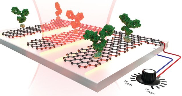
Conceptual view of the graphene biosensor. An infrared beam excites a plasmon resonance across the graphene nanoribbons. Protein sensing is achieved by changing the voltage applied to the graphene and detecting a plasmon resonance spectral shift accompanied by narrow dips corresponding to the molecular vibration bands of the protein. (credit: Daniel Rodrigo et al./Science)

Resonant vibrations

With the new graphene method, the target proteins to be analyzed are attached to the graphene surface. “We pattern nanostructures on the graphene surface by bombarding it with electron beams and etching it with oxygen ions,” said Daniel Rodrigo, co-author of the publication. “When the light arrives, the electrons in graphene nanostructures begin to oscillate. This phenomenon, known as ‘localized surface plasmon resonance,’ serves to concentrate light into tiny spots, which are comparable with the [tiny] dimensions of the target molecules. It is then possible to detect nanometric structures.”

This process can also reveal the nature of the bonds connecting the atoms that the molecule is composed of. When a molecule vibrates, it does so in a range of frequencies, which are generated by the bonds connecting the different atoms. To detect these frequencies,  the researchers “tuned” the graphene to different frequencies by applying voltage, which is not possible with current sensors. Making graphene’s electrons oscillate in different ways makes it possible to “read” all the vibrations of the molecule on its surface. “It gave us a full picture of the molecule,” said co-author Hatice Altug.

According to the researchers, this simple method shows that it is possible to conduct a complex analysis using only one device, while it normally requires many different ones, and without stressing or modifying the biological sample. “The method should also work for polymers, and many other substances,” she added.


Abstract of Mid-infrared plasmonic biosensing with graphene

Infrared spectroscopy is the technique of choice for chemical identification of biomolecules through their vibrational fingerprints. However, infrared light interacts poorly with nanometric-size molecules. We exploit the unique electro-optical properties of graphene to demonstrate a high-sensitivity tunable plasmonic biosensor for chemically specific label-free detection of protein monolayers. The plasmon resonance of nanostructured graphene is dynamically tuned to selectively probe the protein at different frequencies and extract its complex refractive index. Additionally, the extreme spatial light confinement in graphene—up to two orders of magnitude higher than in metals—produces an unprecedentedly high overlap with nanometric biomolecules, enabling superior sensitivity in the detection of their refractive index and vibrational fingerprints. The combination of tunable spectral selectivity and enhanced sensitivity of graphene opens exciting prospects for biosensing.

Omnidirectional wireless charging up to half a meter away from a power source

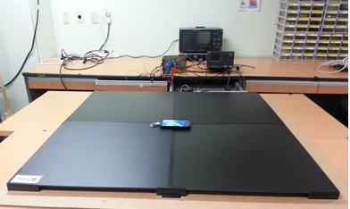
Omnidirectional wireless-charging system can charge multiple numbers of mobile devices simultaneously in a one-cubic-meter range. Above: charging transmitter; below: a Samsung Galaxy Note with embedded receiver. (credit: KAIST)

A group of researchers at KAIST in Korea has developed a wireless-power transfer (WPT) technology that allows mobile devices in the “Wi-Power” zone (within 0.5 meters from the power source) to be charged at any location and in any direction and orientation, tether-free.

The WPT system is capable of charging 30 smartphones with a power capacity of one watt each or 5 laptops with 2.4 watts.

The research team used its Dipole Coil Resonance System (DCRS) to induce magnetic fields, composed of two (transmitting and receiving) magnetic dipole coils, placed in parallel. Each coil has a ferrite core and is connected with a resonant capacitor.

Current wireless-power technologies require close contact with a charging pad and are limited to a fixed position.

The research was published in the June 2015 on-line issue of IEEE Transactions on Power Electronics.


KAIST | KAIST Omnidirectional Wireless Smartphone Charger at 1m


Abstract of Six Degrees of Freedom Mobile Inductive Power Transfer by Crossed Dipole Tx and Rx Coils

Crossed dipole coils for the wide-range 3-D omnidirectional inductive power transfer (IPT) are proposed. Free positioning of a plane receiving (Rx) coil is obtained for an arbitrary direction within 1m from a plane transmission (Tx) coil. Both the Tx and Rx coils consist of crossed dipole coils with an orthogonal phase difference; hence, a rotating magnetic field is generated from the Tx, which enables the Rx to receive power vertically or horizontally. Thus, the 3-D omnidirectional IPT is first realized for both the plate type Tx and Rx coils, which is crucial for practical applications where volumetric coil structure is highly prohibited. This optimized configuration of coils has been obtained through a general classification of power transfer and searching for mathematical constraints on multi-D omnidirectional IPT. Conventional loop coils are thoroughly analyzed and verified to be inadequate for the plate-type omnidirectional IPT in this paper. Simulation-based design of the proposed crossed dipole coils for a uniform magnetic field distribution is provided, and the 3-D omnidirectional IPT is experimentally verified by prototype Rx coils for a wireless power zone of 1 m3 with a prototype Tx coil of 1 m2 at an operating frequency of 280 kHz, meeting the Power Matters Alliance (PMA). The maximum overall efficiency was 33.6% when the input power was 100 W.

Creating DNA-based nanostructures without water

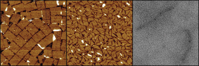
Three different DNA nanostructures assembled at room temperature in water-free glycholine (left) and in 75 percent glycholine-water mixture (center and right). The structures are (from left to right) a tall rectangle two-dimensional DNA origami, a triangle made of single-stranded tails, and a six-helix bundle three-dimensional DNA origami (credit: Isaac Gállego).

Researchers at the Georgia Institute of Technology have discovered an new process for assembling DNA nanostructures in a water-free solvent, which may allow for fabricating more complex nanoscale structures — especially, nanoelectronic chips based on DNA.

Scientists have been using DNA to construct sophisticated new structures from nanoparticles (such as a recent development at Brookhaven National Labs reported by KurzweilAI May 26), but the use of DNA has required a water-based environment. That’s because DNA naturally functions inside the watery environment of living cells. However, the use of water limited the types of structures that are possible.

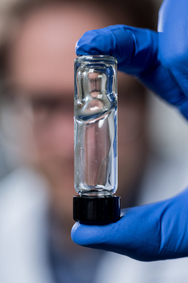
The viscosity of a new solvent used for assembling DNA nanostructures (credit: Rob Felt)

In addition, the Georgia Tech researchers discovered that, paradoxically, adding a small amount of water to their water-free solvent during the assembly process (and removing it later) increases the assembly rate. It could also allow for even more complex structures, by reducing the problem of DNA becoming trapped in unintended structures by aggregation (clumping).

The new solvent they used is known as glycholine, a mixture of glycerol (used for sweetening and preserving food) and choline chloride, but the researchers are exploring other materials.

The solvent system could improve the combined use of metallic nanoparticles and DNA based materials at room temperature. The solvent’s low volatility could also allow for storage of assembled DNA structures without the concern that a water-based medium would dry out.

The research on water-free solvents grew out of Georgia Tech researchers’ studies in the origins of life. They wondered if the molecules necessary for life, such as the ancestor of DNA, could have developed in a water-free solution. In some cases, they found, the chemistry necessary to make the molecules of life would be much easier without water being present.

Sponsored by the National Science Foundation and NASA, the research will be published as the cover story in Volume 54, Issue 23 of the journal Angewandte Chemie International Edition.

* The assembly rate of DNA nanostructures can be very slow, and depends strongly on temperature. Raising the temperature increases this rate, but temperatures that are too high can cause the DNA structures to fall apart. The solvent system developed at Georgia Tech adds a new level of control over DNA assembly. DNA structures assemble at lower temperatures in this solvent, and adding water can adjust the solvent’s viscosity (resistance to flow), which allows for faster assembly compared to the water-free version of the solvent.


Abstract of Folding and Imaging of DNA Nanostructures in Anhydrous and Hydrated Deep-Eutectic Solvents

There is great interest in DNA nanotechnology, but its use has been limited to aqueous or substantially hydrated media. The first assembly of a DNA nanostructure in a water-free solvent, namely a low-volatility biocompatible deep-eutectic solvent composed of a 4:1 mixture of glycerol and choline chloride (glycholine), is now described. Glycholine allows for the folding of a two-dimensional DNA origami at 20 °C in six days, whereas in hydrated glycholine, folding is accelerated (≤3 h). Moreover, a three-dimensional DNA origami and a DNA tail system can be folded in hydrated glycholine under isothermal conditions. Glycholine apparently reduces the kinetic traps encountered during folding in aqueous solvent. Furthermore, folded structures can be transferred between aqueous solvent and glycholine. It is anticipated that glycholine and similar solvents will allow for the creation of functional DNA structures of greater complexity by providing a milieu with tunable properties that can be optimized for a range of applications and nanostructures.

Next-generation energy-efficient light-based computers

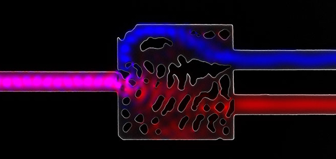
Infrared light enters this silicon structure from the left. The cut-out patterns, determined by an algorithm, route two different wavelengths of this light into the two pathways on the right. (credit: Alexander Piggott)

Stanford University engineers have developed a new design algorithm that can automate the process of designing optical interconnects, which could lead to faster, more energy-efficient computers that use light rather than electricity for internal data transport.

Light can transmit more data while consuming far less power than electricity. According to a study by David Miller, the MIT W.M. Keck Foundation Professor of Electrical Engineering, up to 80 percent of microprocessor power is consumed by sending data over interconnects (wires that connect chips).

In addition, “for chip-scale links, light can carry more than 20 times as much data,” said Stanford graduate student Alexander Y. Piggott, lead author of a Nature Photonics article.

However, designing optical interconnects (using silicon fiber-optics cables) is complex and requires custom design for each interconnect. Given that thousands of interconnects are needed for each electronic system, optical data transport has remained impractical.

Optimized design of optical interconnects

Now the Stanford engineers believe they’ve broken that bottleneck by inventing what they call an “inverse design algorithm.” It works as the name suggests: the engineers specify what they want the optical circuit to do, and the software provides the details of how to fabricate a silicon structure to perform the task.

The wavelength demultiplexer developed by the Stanford team comprised one input waveguide, two output waveguides, and a chip for switching outputs based on incoming wavelengths (credit: Alexander Y. Piggott et al./Nature Photonics)

“We used the algorithm to design a working optical circuit and made several copies in our lab,” said Jelena Vuckovic, a Stanford professor of electrical engineering and senior author of the article.

The optical circuit they created was a silicon wavelength demultiplexer (which splits incoming light into multiple channels based on the wavelengths of the light). The device split 1,300 nm and 1,550 nm light from an input waveguide into two output waveguides.

(“Multiplexing” allows for multiple signals to be transmitted over a thin fiber-optic cable, which is how the Internet and cable television is able to transmit massive amounts of data, not possible with wires.)

The engineers note that once the algorithm has calculated the proper shape for the task, standard scalable industrial processes can be used to transfer that pattern onto silicon. The device footprint is only 2.8 x 2.8 micrometers, making this the smallest dielectric wavelength splitter to date.

The researchers envision other potential applications for their inverse design algorithm, including high-bandwidth optical communications, compact microscopy systems, and ultra-secure quantum communications.


Abstract of Inverse design and demonstration of a compact and broadband on-chip wavelength demultiplexer

Integrated photonic devices are poised to play a key role in a wide variety of applications, ranging from optical interconnects and sensors to quantum computing. However, only a small library of semi-analytically designed devices is currently known. Here, we demonstrate the use of an inverse design method that explores the full design space of fabricable devices and allows us to design devices with previously unattainable functionality, higher performance and robustness, and smaller footprints than conventional devices. We have designed a silicon wavelength demultiplexer that splits 1,300 nm and 1,550 nm light from an input waveguide into two output waveguides, and fabricated and characterized several devices. The devices display low insertion loss (∼2 dB), low crosstalk (<−11 dB) and wide bandwidths (>100 nm). The device footprint is 2.8 × 2.8 μm2, making this the smallest dielectric wavelength splitter.

Improving the experience of the audience with digital instruments

Virtual content being displayed on stage and overlapping the instruments and the performers (credit: Florent Berthaut)

University of Bristol researchers have developed a new augmented-reality display that allows audiences to better appreciate digital musical performances

The research team from the University’s Bristol Interaction and Graphics (BIG) has been investigating how to improve the audiences experience during performances with digital musical instruments, which are played by manipulating buttons, mich, and various other controls.

Funded by a Marie Curie grant, the IXMI project, led by Florent Berthaut, aims to show the mechanisms of digital instruments, using 3D virtual content and mixed-reality displays.

Their first creation Reflets is a mixed-reality environment that allows for displaying virtual content anywhere on stage, even overlapping the instruments or the performers. It does not require the audience to wear glasses or to use their smartphones to see the augmentations, which remain consistent at all positions in the audience.

Reflets relies on combining the audience and stage spaces using reflective transparent surfaces and having the audience and performers reveal the virtual content by intersecting it with their bodies or physical props.

The research is being presented at the 15th International Conference on New Interfaces for Musical Expression (NIME) in the U.S. [May 31 -- June 3].


BristolIG | Ixmi: Improving the experience of the audience with digital instruments

A 99% biodegradable computer chip

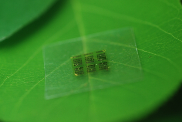
A cellulose nanofibril (CNF) computer chip shown on a leaf (credit: Yei Hwan Jung, Wisconsin Nano Engineering Device Laboratory)

University of Wisconsin-Madison and U.S. Department of Agriculture Forest Products Laboratory (FPL) researchers have jointly developed a wood chip in an effort to alleviate the environmental burden* of electronic devices.

Well, actually, a wood-substrate-based semiconductor chip. They replaced the silicon substrate portion in a conventional chip with environment-friendly cellulose nanofibril (CNF). CNF is a flexible, biodegradable material made from wood, as the researchers note in an open-access paper published May 26 in the journal Nature Communications.

“[More than 99%] of the material in a chip is support,” said Zhiyong Cai, project leader of an engineering composite science research group at FPL. With the new substrate, the chips are “so safe you can put them in the forest and fungus will degrade it. They become as safe as fertilizer.”

The new material is especially important for microwave chips (such as those used in mobile phones) made with gallium arsenide, which is especially difficult to fabricate on foreign substrates. That’s because of the small feature sizes and high temperature processes required for high performance.

Cai’s group addressed two key barriers to using wood-derived materials in an electronics setting: surface roughness and thermal expansion. “You don’t want it to expand or shrink too much. Wood is a natural hydroscopic [water-absorbing] material and could attract moisture from the air and expand,” Cai says. “With an epoxy coating on the surface of the CNF, we solved both [problems].”

* In 2007, it was estimated that over 426,000 cell phones (most of them were still functional) and 112,000 computers were discarded every day in the US, totalling 3.2 million tons of electronic waste generated per year, the researcher note in the paper.


Abstract of High-performance green flexible electronics based on biodegradable cellulose nanofibril paper

Today’s consumer electronics, such as cell phones, tablets and other portable electronic devices, are typically made of non-renewable, non-biodegradable, and sometimes potentially toxic (for example, gallium arsenide) materials. These consumer electronics are frequently upgraded or discarded, leading to serious environmental contamination. Thus, electronic systems consisting of renewable and biodegradable materials and minimal amount of potentially toxic materials are desirable. Here we report high-performance flexible microwave and digital electronics that consume the smallest amount of potentially toxic materials on biobased, biodegradable and flexible cellulose nanofibril papers. Furthermore, we demonstrate gallium arsenide microwave devices, the consumer wireless workhorse, in a transferrable thin-film form. Successful fabrication of key electrical components on the flexible cellulose nanofibril paper with comparable performance to their rigid counterparts and clear demonstration of fungal biodegradation of the cellulose-nanofibril-based electronics suggest that it is feasible to fabricate high-performance flexible electronics using ecofriendly materials.

Medical ‘millirobots’ could replace invasive surgery

Cross-section: three-component Gauss gun before (top) and after (bottom) firing (credit: Aaron T. Becker et al./Proceedings of the IEEE)

University of Houston researchers have developed a concept for MRI-powered millimeter-size “millirobots” that could one day perform unprecedented minimally invasive medical treatments.

This technology could be used to treat hydrocephalus, for example. Current treatments require drilling through the skull to implant pressure-relieving shunts, said Aaron T. Becker, assistant professor of electrical and computer engineering at the University of Houston.

But MRI scanners alone don’t produce enough force to pierce tissues (or insert needles). So the researchers drew upon the principle of the “Gauss gun.”


K&J Magnetics | Gauss Gun Demonstrations

Here’s how the a Gauss gun works: a single steel ball rolls down a chamber, setting off a chain reaction when it smashes into the next ball, etc., until the last ball flies forward, moving much more quickly the initial ball.

Based on that concept, the researchers imagine a medical robot with a barrel self-assembled from three small high-impact 3D-printed plastic components, with slender titanium rod spacers separating two steel balls.

Millirobot components (credit: Aaron T. Becker et al./Proceedings of the IEEE)

Aaron T. Becker, assistant professor of electrical and computer engineering at the University of Houston, said the potential technology could be used to treat hydrocephalus and other conditions, allowing surgeons to avoid current treatments that require cutting through the skull to implant pressure-relieving shunts.

Becker was first author of a paper presented at ICRA, the conference of the IEEE Robotics and Automation Society, nominated for best conference paper and best medical robotics paper.

“Hydrocephalus, among other conditions, is a candidate for correction by our millirobots because the ventricles are fluid-filled and connect to the spinal canal,” Becker said. “Our noninvasive approach would eventually require simply a hypodermic needle or lumbar puncture to introduce the components into the spinal canal, and the components could be steered out of the body afterwards.”

Future work will focus on exploring clinical context, miniaturizing the device, and optimizing material selection.


Abstract of Toward Tissue Penetration by MRI-powered Millirobots Using a Self-Assembled Gauss Gun

MRI-based navigation and propulsion of millirobots is a new and promising approach for minimally invasive therapies. The strong central field inside the scanner, however, precludes torque-based control. Consequently, prior propulsion techniques have been limited to gradient-based pulling through fluid-filled body lumens. This paper introduces a technique for generating large impulsive forces that can be used to penetrate tissue. The approach is based on navigating multiple robots to a desired location and using self-assembly to trigger the conversion of magnetic potential energy into sufficient kinetic energy to achieve penetration. The approach is illustrated through analytical modeling and experiments in a clinical MRI scanner.

New tech keeps your smart phone charged for 30 percent longer

(credit: iStock)

Engineers  at The Ohio State University claim they have created a circuit that makes cell phone batteries last up to 30 percent longer on a single charge. The trick: it converts some of the radio signals emanating from a phone into direct current (DC) power, which then charges the phone’s battery, they state.

This new technology can be built into a cell phone case, adding minimal bulk and weight.

“When we communicate with a cell tower or Wi-Fi router, so much energy goes to waste,” explained Chi-Chih Chen, research associate professor of electrical and computer engineering. “We recycle some of that wasted energy back into the battery.”

“Our technology is based on harvesting energy directly from the source, explained Robert Lee, professor of electrical and computer engineering. By Lee’s reckoning, nearly 97 percent of cell phone signals never reach a destination and are simply lost. Some of the that energy can be captured.

The idea is to siphon off just enough of the radio signal to noticeably slow battery drain, but not enough to degrade voice quality or data transmission. Cell phones broadcast in all directions at once to reach the nearest cell tower or Wi-Fi router. Chen and his colleagues came up with a system that identifies which radio signals are being wasted. It works only when a phone is transmitting.

Next, the engineers want to insert the device into a “skin” that sticks directly to a phone, or better, partner with a manufacturer to build it directly into a phone, tablet or other portable electronic device.

UPDATE June 6: Responding to a request for more information on energy harvesting, we received the following statement from Will Zell, CEO of licensee Nikola Labs: “Nikola Labs has a limit to the technical details we are able to share until our patents are published.”

A chip implanted under the skin allows for precise, real-time medical monitoring

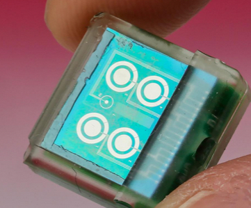
Under-the-skin chip (credit: EPFL)

A tiny (one-centimeter-square) biosensor chip developed at EPFL is designed to be implanted under your skin to continuously monitor concentrations of pH, temperature, and metabolism-related molecules like glucose, lactate and cholesterol, as well as some drugs.

The chip would replace blood work, which may take  hours — or even days — for analysis and is a limited snapshot of conditions at the moment the blood is drawn.

Developer Sandro Carrara unveiled the chip Tuesday (May 26) at the International Symposium on Circuits and Systems (ISCAS) in Lisbon.

The electrochemical sensors work with or without enzymes, which means the device can react to a wide range of compounds, and it can do so for several days or even weeks.

Wireless power and monitoring

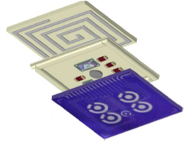
Implantable biosensor chip with three layers: a passive sensing platform (bottom), integrated circuits (middle) to analyze electrochemical measurements and generate a Bluetooth signal, and a coil (top) for through-the-skin data transmission and power via an external battery (credit: Camilla Baj-Rossi et al./IEEE Transactions on Biomedical Circuits and Systems)

The biochip contains three main components: a circuit with six sensors, a control unit that analyzes incoming signals, and a Bluetooth module for sending the results immediately to a mobile phone.

It also has an induction coil that wirelessly draws power from an external battery attached to the skin by a patch.

To ensure biocompatibility, an epoxy-enhanced polyurethane membrane was used to cover the device.

The chip was successfully tested in vivo on mice at the Institute for Research in Biomedicine (IRB) in Bellinzona, where researchers were able to constantly monitor glucose and paracetamol levels without a wire tracker getting in the way of the animals’ daily activities.

The results were promising, so clinical tests on humans could take place in three to five years — especially since the procedure is minimally invasive, the researchers say.

“Knowing the precise and real-time effect of drugs on the metabolism is one of the keys to the type of personalised, precision medicine that we are striving for,” said Carrara.