A battery-free origami robot powered and controlled by external magnetic fields

Wirelessly powered and controlled magnetic folding robot arm can grasp and bend (credit: Wyss Institute at Harvard University)

Harvard University researchers have created a battery-free, folding robot “arm” with multiple “joints,” gripper “hand,” and actuator “muscles” — all powered and controlled wirelessly by an external resonant magnetic field.

The design is inspired by the traditional Japanese art of origami (used to transform a simple sheet of paper into complex, three-dimensional shapes through a specific pattern of folds, creases, and crimps). The prototype device is capable of complex, repeatable movements at millimeter to centimeter scales.

The research, by scientists at the Wyss Institute for Biologically Inspired Engineering and the John A. Paulson School of Engineering and Applied Sciences (SEAS), is reported in Science Robotics.

How it works

Design of small-scale-structure prototype of wirelessly controlled robotic arm (credit: Mustafa Boyvat et al./Science Robotics)

The researchers designed a 0.8-gram prototype small-scale-structure* prototype robotic “arm” capable of bending and opening or closing a gripper around an object. The “arm” is constructed with a special origami-like pattern that uses hinges (“joints”) to permit it to bend. There is also a “hand” (gripper — left panel in above image) that opens or closes.

To power the device, an external coil with its own power source (see video below) is used to generate a low-frequency magnetic field that induces an electrical current in three magnetic coils. The current heats the spiral-wire shape-memory-alloy actuator wires (coiled wire shown in inset above). That causes the actuator wires (“muscles”) to contract, making the attached nearby “joints” bend, and folding the robot body.

Mechanism of the origami gripper (for small-scale prototype design). (Left) The coil SMA actuator pushes the center link connected to both fingers and the gripper opens fingers, enabled by dynamic folding at the joints (left). The plate spring, which is a passive compression spring, pulls the link back as the gripper closes the fingers, again by rotations at folding joints (center). (Right) A photo of the gripper showing the SMA actuator wire attached at the center link. (credit: Mustafa Boyvat et al./Science Robotics)

By changing the resonant frequency of the external electromagnetic field, the two longer actuator wires (coiled wires shown in above illustration) are instead heated and stretched, opening the gripper (“hand”).

In both cases, when the external field-induced current stops, the actuators relax, springing back to their “memory” positions and causing the robot body to straighten out or the gripper’s outer triangles to close.

Minimally invasive medicine and surgery applications

As an example of a practical future application, instead of having an uncomfortable endoscope put down their throat to assist a doctor with surgery, a patient could just swallow a micro-robot that could move around and perform simple tasks, like holding tissue or filming, powered by a coil outside their body.

Using a much larger source coil — on the order of yards in diameter — could enable wireless, battery-free communication between multiple “smart” objects in a room or building.

“Medical devices today are commonly limited by the size of the batteries that power them, whereas these remotely powered origami robots can break through that size barrier and potentially offer entirely new, minimally invasive approaches for medicine and surgery in the future,” says Wyss Founding Director Donald Ingber, who is also the Judah Folkman Professor of Vascular Biology at Harvard Medical School and the Vascular Biology Program at Boston Children’s Hospital, as well as a Professor of Bioengineering at Harvard’s School of Engineering and Applied Sciences.

This work was supported by the National Science Foundation, the U.S. Army Research Laboratory, and the Swiss National Science Foundation.

* A large-scale-structure prototype version has minor differences, including 12-cm folding lines vs. 1.7-cm folding lines in the smaller version.

Wyss Institute | Battery-Free Folding Robots


Abstract of Addressable wireless actuation for multijoint folding robots and devices

“Printing” robots and other complex devices through a process of origami-like folding is an emerging and promising manufacturing method due to the inherent simplicity and low cost of folding-based assembly. Folding is used in this class of device to create both complex static structures and flexure-based compliant mechanisms. Dependency on batteries to power these folds with no external wires is a hurdle to giving small-scale folding robots and devices functionality. We demonstrate a battery-free wireless folding method for dynamic multijoint structures, achieving addressable folding motions—both individual and collective folding—using only basic passive electronic components on the device. The method is based on electromagnetic power transmission and resonance selectivity for actuation of resistive shape memory alloy actuators without the need for physical connection or line of sight. We demonstrate the utility of this approach using two folded devices at different sizes using different circuit approaches.

New system allows near-zero-power sensors to communicate data over long distances

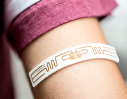
This low-cost, flexible epidermal medical-data patch prototype successfully transmitted information at up to 37500 bits per second across a 3,300-square-feet atrium. (credit: Dennis Wise/University of Washington)

University of Washington (UW) researchers have developed a low-cost, long-range data-communication system that could make it possible for medical sensors or billions of low-cost “internet of things” objects to connect via radio signals at long distances (up to 2.8 kilometers) and with 1000 times lower required power (9.25 microwatts in an experiment) compared to existing technologies.

“People have been talking about embedding connectivity into everyday objects … for years, but the problem is the cost and power consumption to achieve this,” said Vamsi Talla, chief technology officer of Jeeva Wireless, which plans to market the system within six months. “This is the first wireless system that can inject connectivity into any device with very minimal cost.”

The new system uses “backscatter,” which uses energy from ambient transmissions (from WiFi, for example) to power a passive sensor that encodes and scatter-reflects the signal. (This article explains how ambient backscatter, developed by UW, works.) Backscatter systems, used with RFID chips, are very low cost, but are limited in distance.

So the researchers combined backscatter with a “chirp spread spectrum” technique, used in LoRa (long-range) wireless data-communication systems.

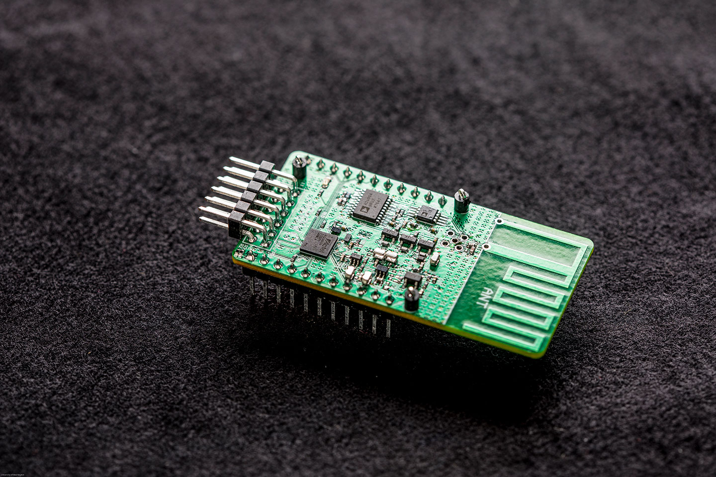
This tiny off-the-shelf spread-spectrum receiver enables extremely-low-power cheap sensors to communicate over long distances. (credit: Dennis Wise/University of Washington)

This new system has three components: a power source (which can be WiFi or other ambient transmission sources, or cheap flexible printed batteries, with an expected bulk cost of 10 to 20 cents each) for a radio signal; cheap sensors (less than 10 cents at scale) that modulate (encode) information (contained in scattered reflections of the signal), and an inexpensive, off-the-shelf spread-spectrum receiver, located as far away as 2.8 kilometers, that decodes the sensor information.

Applications could include, for example, medical monitoring devices that wirelessly transmit information about a heart patient’s condition to doctors; sensor arrays that monitor pollution, noise, or traffic in “smart” cities; and farmers looking to measure soil temperature or moisture, who could affordably blanket an entire field to determine how to efficiently plant seeds or water.

The research team built a contact lens prototype and a flexible epidermal patch that attaches to human skin, which successfully used long-range backscatter to transmit information across a 3300-square-foot building.

The research, which was partially funded by the National Science Foundation, is detailed in an open-access paper presented Sept. 13, 2017 at UbiComp 2017. More information: longrange@cs.washington.edu.


UW (University of Washington) | UW team shatters long-range communication barrier for devices that consume almost no power


Abstract of LoRa Backscatter: Enabling The Vision of Ubiquitous Connectivity

The vision of embedding connectivity into billions of everyday objects runs into the reality of existing communication technologies — there is no existing wireless technology that can provide reliable and long-range communication at tens of microwatts of power as well as cost less than a dime. While backscatter is low-power and low-cost, it is known to be limited to short ranges. This paper overturns this conventional wisdom about backscatter and presents the first wide-area backscatter system. Our design can successfully backscatter from any location between an RF source and receiver, separated by 475 m, while being compatible with commodity LoRa hardware. Further, when our backscatter device is co-located with the RF source, the receiver can be as far as 2.8 km away. We deploy our system in a 4,800 ft2 (446 m2) house spread across three floors, a 13,024 ft2 (1210 m2) office area covering 41 rooms, as well as a one-acre (4046 m2) vegetable farm and show that we can achieve reliable coverage, using only a single RF source and receiver. We also build a contact lens prototype as well as a flexible epidermal patch device attached to the human skin. We show that these devices can reliably backscatter data across a 3,328 ft2 (309 m2) room. Finally, we present a design sketch of a LoRa backscatter IC that shows that it costs less than a dime at scale and consumes only 9.25 &mgr;W of power, which is more than 1000x lower power than LoRa radio chipsets.

Miniature MRI simulator chip could help diagnose and treat diseases in the body at sub-millimeter precision

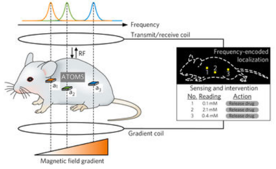
Illustration of an ATOMS microchip localized within the gastrointestinal tract (not to scale; a prototype measures just 0.7 cubic millimeters). The microchip contains a magnetic field sensor, integrated antennas, a wireless powering device, and a circuit that adjusts its radio frequency signal based on the magnetic field strength and wirelessly relays the chip’s precise location. (credit: Ella Marushchenko/Caltech)

Caltech researchers have developed a “Fantastic Voyage” style prototype microchip that could one day be used in “smart pills” to diagnose and treat diseases when inserted into the human body.

Called ATOMS (addressable transmitters operated as magnetic spins), the microchips could one day monitor a patient’s gastrointestinal tract, blood, or brain, measuring factors that indicate a patient’s health — such as pH, temperature, pressure, and sugar concentrations — with sub-millimeter localization and relay that information to doctors. Or the devices could even be instructed to release drugs at precise locations.

An open access paper describing the new device appears in the September issue of the journal Nature Biomedical Engineering. The lead author is Manuel Monge, who now works at Elon Musk’s new Neuralink company.

The ATOMS microchips, proven to work in tests with mice, mimic the way nuclear spins in atoms in the body resonate to magnetic fields in a magnetic resonance imaging (MRI) machine and can be precisely identified and localized within the body. Similarly, the ATOMS devices resonate at different frequencies depending on where they are in a magnetic field. (credit: Manuel Monge et al./ Nature Biomedical Engineering)


Abstract of Localization of Microscale Devices In Vivo using Addressable Transmitters Operated as Magnetic Spins

The function of miniature wireless medical devices, such as capsule endoscopes, biosensors and drug-delivery systems, depends critically on their location inside the body. However, existing electromagnetic, acoustic and imaging-based methods for localizing and communicating with such devices suffer from limitations arising from physical tissue properties or from the performance of the imaging modality. Here, we embody the principles of nuclear magnetic resonance in a silicon integrated-circuit approach for microscale device localization. Analogous to the behaviour of nuclear spins, the engineered miniaturized radio frequency transmitters encode their location in space by shifting their output frequency in proportion to the local magnetic field; applied field gradients thus allow each device to be located precisely from its signal’s frequency. The devices are integrated in circuits smaller than 0.7 mm3 and manufactured through a standard complementary-metal-oxide-semiconductor process, and are capable of sub-millimetre localization in vitro and in vivo. The technology is inherently robust to tissue properties, scalable to multiple devices, and suitable for the development of microscale devices to monitor and treat disease.

A single-molecule room-temperature transistor made from 14 atoms

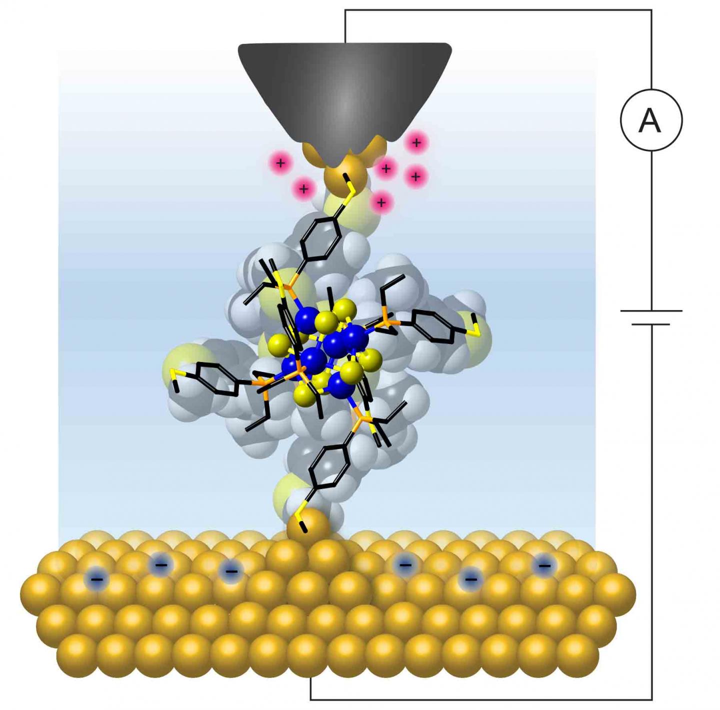
Columbia researchers wired a single molecule consisting of 14 atoms connected to two gold electrodes to show that it performs as a transistor at room temperature. (credit: Bonnie Choi/Columbia University)

Columbia Engineering researchers have taken a key step toward atomically precise, reproducible transistors made from single molecules and operating at room temperature — a major goal in the field of molecular electronics.

The team created a two-terminal transistor with a diameter of about 0.5 nanometers and core consisting of just 14 atoms. The device can reliably switch from insulator to conductor when charge is added or removed, one electron at a time (known as “current blockade”).*

The research was published in the journal Nature Nanotechnology.

Controllable structure with atomic precision

“With these molecular clusters, we have complete control over their structure with atomic precision and can change the elemental composition and structure in a controllable manner to elicit certain electrical response,” says Latha Venkataraman, leader of the Columbia research team.

The researchers plan to design improved molecular cluster systems with better electrical performance (such as higher on/off current ratio and different accessible states) and increase the number of atoms in the cluster core, while maintaining the atomic precision and uniformity of the compound.

Other studies have created quantum dots to produce similar effects, but the dots are much larger and not uniform in size, and the results have not been reproducible. The ultimate size reduction would be single-atom transistors, but they require ultra-cold temperatures (minus 196 degrees Celsius in this case, for example).

The single molecule’s 14-atom core structure comprises cobalt (blue) and sulfur (yellow) atoms (left) and ethyl-4-(methylthio)phenyl phosphine atoms, used to wire the cluster into a junction (right). (credit: Bonnie Choi/Columbia University)

* The researchers used a scanning tunneling microscope technique that they pioneered to make junctions comprising a single cluster connected to the two gold electrodes, which enabled them to characterize its electrical response as they varied the applied bias voltage. The technique allows them to fabricate and measure thousands of junctions with reproducible transport characteristics. The team worked with small inorganic molecular clusters that were identical in shape and size, so they knew exactly — down to the atomic scale — what they were measuring. The team evaluated the performance of the diode by the on/off ratio — the ratio between the current flowing through the device when it is switched on and the residual current still present in its “off” state. At room temperature, they observed a high on/off ratio of about 600 in single-cluster junctions, higher than any other single-molecule devices measured to date.


Abstract of Room-temperature current blockade in atomically defined single-cluster junctions

Fabricating nanoscopic devices capable of manipulating and processing single units of charge is an essential step towards creating functional devices where quantum effects dominate transport characteristics. The archetypal single-electron transistor comprises a small conducting or semiconducting island separated from two metallic reservoirs by insulating barriers. By enabling the transfer of a well-defined number of charge carriers between the island and the reservoirs, such a device may enable discrete single-electron operations. Here, we describe a single-molecule junction comprising a redox-active, atomically precise cobalt chalcogenide cluster wired between two nanoscopic electrodes. We observe current blockade at room temperature in thousands of single-cluster junctions. Below a threshold voltage, charge transfer across the junction is suppressed. The device is turned on when the temporary occupation of the core states by a transiting carrier is energetically enabled, resulting in a sequential tunnelling process and an increase in current by a factor of ∼600. We perform in situ and ex situ cyclic voltammetry as well as density functional theory calculations to unveil a two-step process mediated by an orbital localized on the core of the cluster in which charge carriers reside before tunnelling to the collector reservoir. As the bias window of the junction is opened wide enough to include one of the cluster frontier orbitals, the current blockade is lifted and charge carriers can tunnel sequentially across the junction.

Astronomers detect 15 high-frequency ‘fast radio bursts’ from distant galaxy

Green Bank Telescope in West Virginia (credit: Geremia/CC)

Using the Green Bank radio telescope, astronomers at Breakthrough Listen, a $100 million initiative to find signs of intelligent life in the universe, have detected 15 brief but powerful “fast radio bursts” (FRBs). These microwave radio pulses are from a mysterious source known as FRB 121102* in a dwarf galaxy about 3 billion light years from Earth, transmitting at record high frequencies (4 to 8 GHz), according to the researchers

This sequence of 14 of the 15 detected fast radio bursts illustrates their dispersed spectrum and extreme variability. The streaks across the colored energy plot are the bursts appearing at different times and different energies because of dispersion caused by 3 billion years of travel through intergalactic space. In the top frequency spectrum, the dispersion has been removed to show the 300 microsecond pulse spike. (credit: Berkeley SETI Research Center)

Andrew Siemion, director of the Berkeley SETI Research Center and of the Breakthrough Listen program, and his team alerted the astronomical community to the high-frequency activity via an Astronomer’s Telegram on Monday evening, Aug. 28.

A schematic illustration of CSIRO’s Parkes radio telescope in Australia receiving a fast radio burst signal in 2014 (credit: Swinburne Astronomy Productions)

First detected in 2007, fast radio bursts are brief, bright pulses of radio emission detected from distant but largely unknown sources.

Breakthrough Starshot’s plan to use powerful laser pulses to propel nano-spacecraft to Proxima Centauri (credit: Breakthrough Initiatives)

Possible explanations for the repeating bursts range from outbursts from magnetars (rotating neutron stars with extremely strong magnetic fields) to directed energy sources — powerful bursts used by extraterrestrial civilizations to power exploratory spacecraft, akin to Breakthrough Starshot’s plan to use powerful laser pulses to propel nano-spacecraft to Earth’s nearest star, Proxima Centauri.

* FRB 121102 was discovered Nov 2, 2014 (hence its name) with the Arecibo radio telescope, and in 2015 it was the first fast radio burst seen to repeat. More than 150 high-energy bursts have been observed so far. (The repetition ruled out the possibility that FRBs were caused by catastrophic events.)


FRB 121102: Detection at 4 – 8 GHz band with Breakthrough Listen backend at Green Bank

On Saturday, August 26 at 13:51:44 UTC we initiated observations of the well-known repeating fast radio burst FRB 121102 [Spitler et al., Nature, 531, 7593 202-205, 2016] using the Breakthrough Listen Digital Backend with the C-band receiver at the Green Bank Telescope. We recorded baseband voltage data across 5.4375 GHz of bandwidth, completely covering the C-band receiver’s nominal 4-8 GHz band [MacMahon et al. arXiv:1707.06024v2]. Observations were conducted over ten 30-minute scans, as detailed in Table 1. Immediately after observations, the baseband data were reduced to form high time resolution (300 us integration) Stokes-I products using a GPU-accelerated spectroscopy suite. These reduced products were searched for dispersed pulses consistent with the known dispersion measure of FRB 121102 (557 pc cm^-3); baseband voltage data were preserved. We detected 15 bursts above our detection threshold of 10 sigma in the first two 30-minute scans, denoted 11A-L and 12A-B in Table 2. In Table 2, we include the detection signal-to-noise ratio (SNR) of each burst, along with a very rough estimate of pulse energy density assuming a 12 Jy system equivalent flux density, 300 us pulse width, and uniform 3800 MHz bandwidth. We note the following phenomenological properties of the detected bursts: 1. Bursts show marked changes in spectral extent, with characteristic spectral structure in the 100 MHz – 1 GHz range. 2. Several bursts appear to peak in brightness at frequencies above 6 GHz.


Single-molecule-level data storage may achieve 100 times higher data density

(credit: iStock)

Scientists at the University of Manchester have developed a data-storage method that could achieve 100 times higher data density than current technologies.*

The system would allow for data servers to operate at the (relatively high) temperature of -213 °C. That could make it possible in the future for data servers to be chilled by liquid nitrogen (-196 °C) — a cooling method that is relatively cheap compared to the far more expensive liquid helium (which requires -269 °C) currently used.

The research provides proof-of-concept that such technologies could be achievable in the near future “with judicious molecular design.”

Huge benefits for the environment

Molecular-level data storage could lead to much smaller hard drives that require less energy, meaning data centers across the globe could be smaller, lower-cost, and a lot more energy-efficient.

Google data centers (credit: Google)

For example, Google currently has 15 data centers around the world. They process an average of 40 million searches per second, resulting in 3.5 billion searches per day and 1.2 trillion searches per year. To deal with all that data, Google had approximately 2.5 million servers in each data center, it was reported in 2016, and that number was likely to rise.

Some reports say the energy consumed at such centers could account for as much as 2 per cent of the world’s total greenhouse gas emissions. This means any improvement in data storage and energy efficiency could also have huge benefits for the environment as well as vastly increasing the amount of information that can be stored.

The research, led by David Mills, PhD, and Nicholas Chilton, PhD, from the School of Chemistry, is published in the journal Nature. “Our aim is to achieve even higher operating temperatures in the future, ideally functioning above liquid nitrogen temperatures,” said Mills.

* The method uses single-molecule magnets, which display “hysteresis” — a magnetic memory effect that is a requirement of magnetic data storage, such as hard drives. Molecules containing lanthanide atoms have exhibited this phenomenon at the highest temperatures to date. Lanthanides are rare earth metals used in all forms of everyday electronic devices such as smartphones, tablets and laptops. The team achieved their results using the lanthanide element dysprosium.


Abstract of Molecular magnetic hysteresis at 60 kelvin in dysprosocenium

Lanthanides have been investigated extensively for potential applications in quantum information processing and high-density data storage at the molecular and atomic scale. Experimental achievements include reading and manipulating single nuclear spins, exploiting atomic clock transitions for robust qubits and, most recently, magnetic data storage in single atoms. Single-molecule magnets exhibit magnetic hysteresis of molecular origin—a magnetic memory effect and a prerequisite of data storage—and so far, lanthanide examples have exhibited this phenomenon at the highest temperatures. However, in the nearly 25 years since the discovery of single-molecule magnets, hysteresis temperatures have increased from 4 kelvin to only about 14 kelvin using a consistent magnetic field sweep rate of about 20 oersted per second, although higher temperatures have been achieved by using very fast sweep rates (for example, 30 kelvin with 200 oersted per second). Here we report a hexa-tert-butyldysprosocenium complex—[Dy(Cpttt)2][B(C6F5)4], with Cpttt = {C5H2tBu3-1,2,4} and tBu = C(CH3)3—which exhibits magnetic hysteresis at temperatures of up to 60 kelvin at a sweep rate of 22 oersted per second. We observe a clear change in the relaxation dynamics at this temperature, which persists in magnetically diluted samples, suggesting that the origin of the hysteresis is the localized metal–ligand vibrational modes that are unique to dysprosocenium. Ab initio calculations of spin dynamics demonstrate that magnetic relaxation at high temperatures is due to local molecular vibrations. These results indicate that, with judicious molecular design, magnetic data storage in single molecules at temperatures above liquid nitrogen should be possible.

Flexible ‘electronic skin’ patch provides wearable health monitoring anywhere on the body

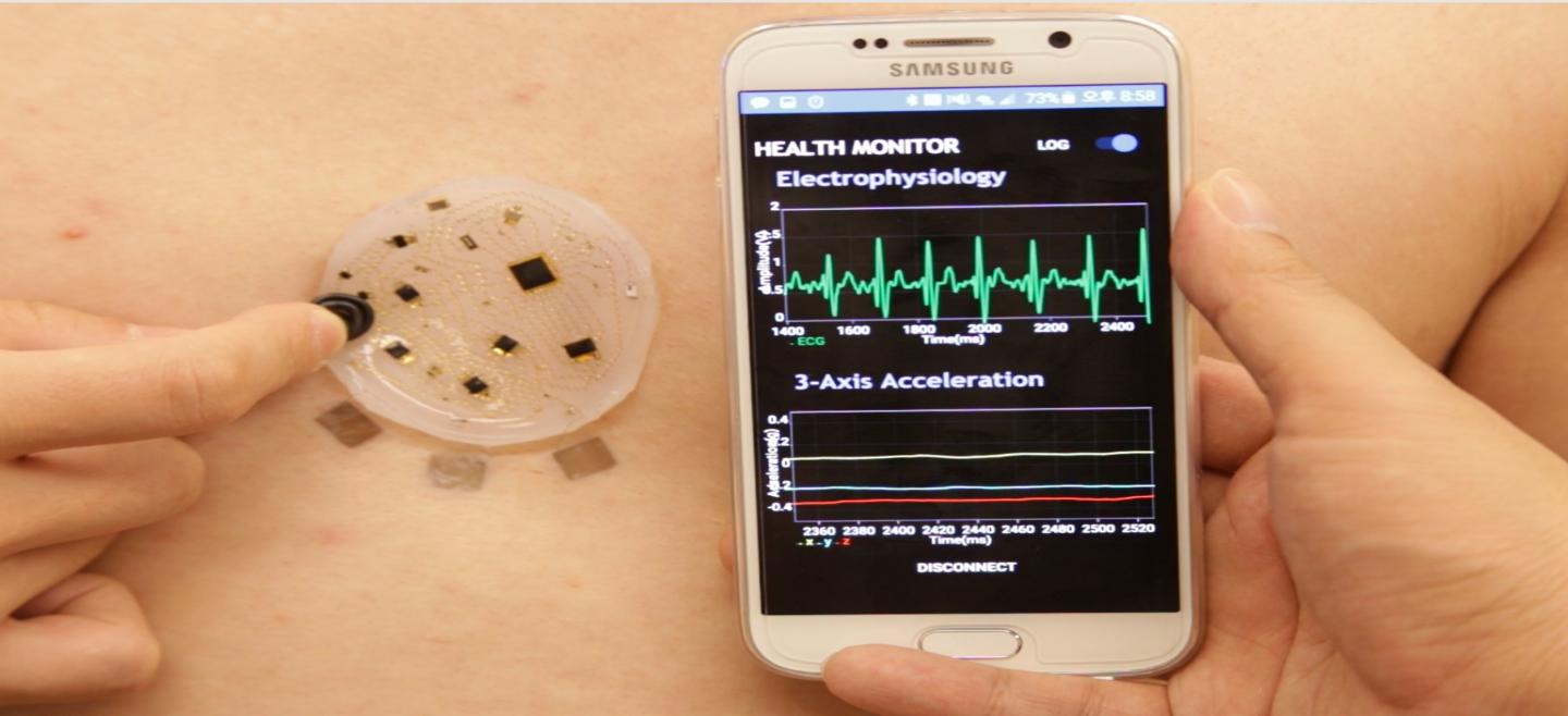
New soft electronic stick-on patch collects, analyzes, and diagnoses biosignals and sends data wirelessly to a mobile app. (credit: DGIST)

A radical new electronic skin monitor developed by Korean and U.S. scientists tracks heart rate, respiration, muscle movement, acceleration, and electrical activity in the heart, muscles, eyes, and brain and wirelessly transmits it to a smartphone, allowing for continuous health monitoring.

KurzweilAI has covered a number of biomedical skin-monitoring devices. This new design is noteworthy because the soft, flexible self-adhesive patch (a soft silicone material about four centimeters or 1.5 inches in diameter) can be instantly stuck just about anywhere on the body as needed — no battery required (it’s powered wirelessly).

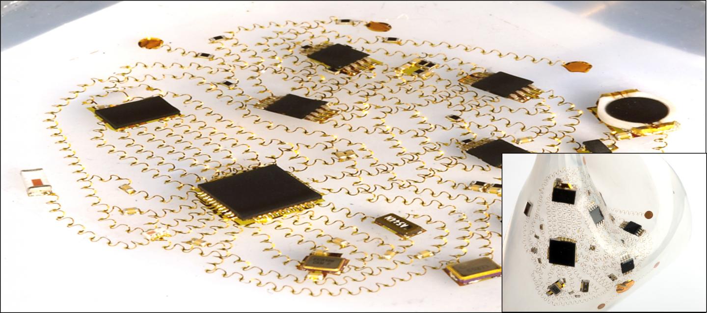
Optical image of the three-dimensional network of helical coils as electrical interconnects for soft electronics. (credit: DGIST)

The patch is designed more like a mattress or creeping vine than a conventional electronic device. It contains about 50 components connected by a network of 250 tiny flexible wire coils embedded in protective silicone. Unlike flat sensors, the tiny helical wire coils, made of gold, chromium and phosphate, are firmly connected to the base only at one end and can stretch and contract like a spring without breaking.

Helical coils serve as 3D electrical interconnects for soft electronics. (credit: DGIST)

The researchers say the microsystem could also be used in soft robotics, virtual reality, and autonomous navigation.

The microsystem was developed by an international team led by Kyung-In Jang, a professor of robotics engineering at South Korea’s Daegu Gyeongbuk Institute of Science and Technology, and John A. Rogers, the director of Northwestern University’s Center for Bio-Integrated Electronics. The research is described in the open-access journal Nature Communications.

“We have several human subject studies ongoing with our medical school at Northwestern — mostly with a focus on health status monitoring in infants,” Rogers told KurzweilAI.


Abstract of Self-assembled three dimensional network designs for soft electronics

Low modulus, compliant systems of sensors, circuits and radios designed to intimately interface with the soft tissues of the human body are of growing interest, due to their emerging applications in continuous, clinical-quality health monitors and advanced, bioelectronic therapeutics. Although recent research establishes various materials and mechanics concepts for such technologies, all existing approaches involve simple, two-dimensional (2D) layouts in the constituent micro-components and interconnects. Here we introduce concepts in three-dimensional (3D) architectures that bypass important engineering constraints and performance limitations set by traditional, 2D designs. Specifically, open-mesh, 3D interconnect networks of helical microcoils formed by deterministic compressive buckling establish the basis for systems that can offer exceptional low modulus, elastic mechanics, in compact geometries, with active components and sophisticated levels of functionality. Coupled mechanical and electrical design approaches enable layout optimization, assembly processes and encapsulation schemes to yield 3D configurations that satisfy requirements in demanding, complex systems, such as wireless, skin-compatible electronic sensors.

How to turn a crystal into an erasable electrical circuit

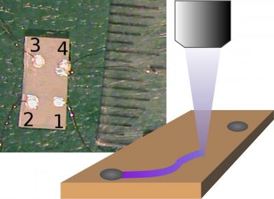
Washington State University researchers used light to write a highly conducting electrical path in a crystal that can be erased and reconfigured. (Left) A photograph of a sample with four metal contacts. (Right) An illustration of a laser drawing a conductive path between two contacts. (credit: Washington State University)

Washington State University (WSU) physicists have found a way to write an electrical circuit into a crystal, opening up the possibility of transparent, three-dimensional electronics that, like an Etch A Sketch, can be erased and reconfigured.

Ordinarily, a crystal does not conduct electricity. But when the researchers heated up crystal strontium titanate under the specific conditions, the crystal was altered so that light made it conductive. The circuit could be erased by heating it with an optical pen.

Schematic diagram of experiment in writing an electrical circuit into a crystal (credit: Washington State University)

The physicists were able to increase the crystal’s conductivity 1,000-fold. The phenomenon occurred at room temperature.

“It opens up a new type of electronics where you can define a circuit optically and then erase it and define a new one,” said Matt McCluskey, a WSU professor of physics and materials science.

The work was published July 27, 2017 in the open-access on-line journal Scientific Reports. The research was funded by the National Science Foundation.


Abstract of Using persistent photoconductivity to write a low-resistance path in SrTiO3

Materials with persistent photoconductivity (PPC) experience an increase in conductivity upon exposure to light that persists after the light is turned off. Although researchers have shown that this phenomenon could be exploited for novel memory storage devices, low temperatures (below 180 K) were required. In the present work, two-point resistance measurements were performed on annealed strontium titanate (SrTiO3, or STO) single crystals at room temperature. After illumination with sub-gap light, the resistance decreased by three orders of magnitude. This markedly enhanced conductivity persisted for several days in the dark. Results from IR spectroscopy, electrical measurements, and exposure to a 405 nm laser suggest that contact resistance plays an important role. The laser was then used as an “optical pen” to write a low-resistance path between two contacts, demonstrating the feasibility of optically defined, transparent electronics.

How to run faster, smarter AI apps on smartphones

(credit: iStock)

When you use smartphone AI apps like Siri, you’re dependent on the cloud for a lot of the processing — limited by your connection speed. But what if your smartphone could do more of the processing directly on your device — allowing for smarter, faster apps?

MIT scientists have taken a step in that direction with a new way to enable artificial-intelligence systems called convolutional neural networks (CNNs) to run locally on mobile devices. (CNN’s are used in areas such as autonomous driving, speech recognition, computer vision, and automatic translation.) Neural networks take up a lot of memory and consume a lot of power, so they usually run on servers in the cloud, which receive data from desktop or mobile devices and then send back their analyses.

The new MIT analytic method can determine how much power a neural network will actually consume when run on a particular type of hardware. The researchers used the method to evaluate new techniques for paring down neural networks so that they’ll run more efficiently on handheld devices.

The new CNN designs are also optimized to run on an energy-efficient computer chip optimized for neural networks that the researchers developed in 2016.

Reducing energy consumption

The new MIT software method uses “energy-aware pruning” — meaning they reduce a neural networks’ power consumption by cutting out the layers of the network that contribute very little to a neural network’s final output and consume the most energy.

Associate professor of electrical engineering and computer science Vivienne Sze and colleagues describe the work in an open-access paper they’re presenting this week (of July 24, 2017) at the Computer Vision and Pattern Recognition Conference. They report that the methods offered up to 73 percent reduction in power consumption over the standard implementation of neural networks — 43 percent better than the best previous method.

Meanwhile, another MIT group at the Computer Science and Artificial Intelligence Laboratory has designed a hardware approach to reduce energy consumption and increase computer-chip processing speed for specific apps, using “cache hierarchies.” (“Caches” are small, local memory banks that store data that’s frequently used by computer chips to cut down on time- and energy-consuming communication with off-chip memory.)**

The researchers tested their system on a simulation of a chip with 36 cores, or processing units. They found that compared to its best-performing predecessors, the system increased processing speed by 20 to 30 percent while reducing energy consumption by 30 to 85 percent. They presented the new system, dubbed Jenga, in an open-access paper at the International Symposium on Computer Architecture earlier in July 2017.

Better batteries — or maybe, no battery?

Another solution to better mobile AI is improving rechargeable batteries in cell phones (and other mobile devices), which have limited charge capacity and short lifecycles, and perform poorly in cold weather.

Recently, DARPA-funded researchers from the University of Houston (and at the University of California-San Diego and Northwestern University) have discovered that quinones — an inexpensive, earth-abundant and easily recyclable material that is low-cost and nonflammable — can address current battery limitations.

“One of these batteries, as a car battery, could last 10 years,” said Yan Yao, associate professor of electrical and computer engineering. In addition to slowing the deterioration of batteries for vehicles and stationary electricity storage batteries, it also would make battery disposal easier because the material does not contain heavy metals. The research is described in Nature Materials.

The first battery-free cellphone that can send and receive calls using only a few microwatts of power. (credit: Mark Stone/University of Washington)

But what if we eliminated batteries altogether? University of Washington researchers have invented a cellphone that requires no batteries. Instead, it harvests 3.5 microwatts of power from ambient radio signals, light, or even the vibrations of a speaker.

The new technology is detailed in a paper published July 1, 2017 in the Proceedings of the Association for Computing Machinery on Interactive, Mobile, Wearable and Ubiquitous Technologies.

The UW researchers demonstrated how to harvest this energy from ambient radio signals transmitted by a WiFi base station up to 31 feet away. “You could imagine in the future that all cell towers or Wi-Fi routers could come with our base station technology embedded in it,” said co-author Vamsi Talla, a former UW electrical engineering doctoral student and Allen School research associate. “And if every house has a Wi-Fi router in it, you could get battery-free cellphone coverage everywhere.”

A cellphone CPU (computer processing unit) typically requires several watts or more (depending on the app), so we’re not quite there yet. But that power requirement could one day be sufficiently reduced by future special-purpose chips and MIT’s optimized algorithms.

It might even let you do amazing things. :)

* Loosely based on the anatomy of the brain, neural networks consist of thousands or even millions of simple but densely interconnected information-processing nodes, usually organized into layers. The connections between nodes have “weights” associated with them, which determine how much a given node’s output will contribute to the next node’s computation. During training, in which the network is presented with examples of the computation it’s learning to perform, those weights are continually readjusted, until the output of the network’s last layer consistently corresponds with the result of the computation. With the proposed pruning method, the energy consumption of AlexNet and GoogLeNet are reduced by 3.7x and 1.6x, respectively, with less than 1% top-5 accuracy loss.

** The software reallocates cache access on the fly to reduce latency (delay), based on the physical locations of the separate memory banks that make up the shared memory cache. If multiple cores are retrieving data from the same DRAM [memory] cache, this can cause bottlenecks that introduce new latencies. So after Jenga has come up with a set of cache assignments, cores don’t simply dump all their data into the nearest available memory bank; instead, Jenga parcels out the data a little at a time, then estimates the effect on bandwidth consumption and latency. 

*** The stumbling block, Yao said, has been the anode, the portion of the battery through which energy flows. Existing anode materials are intrinsically structurally and chemically unstable, meaning the battery is only efficient for a relatively short time. The differing formulations offer evidence that the material is an effective anode for both acid batteries and alkaline batteries, such as those used in a car, as well as emerging aqueous metal-ion batteries.

Neural stem cells steered by electric fields can repair brain damage

Electrical stimulation of the rat brain to move neural stem cells (credit: Jun-Feng Feng et al./ Stem Cell Reports)

Electric fields can be used to guide transplanted human neural stem cells — cells that can develop into various brain tissues — to repair brain damage in specific areas of the brain, scientists at the University of California, Davis have discovered.

It’s well known that electric fields can locally guide wound healing. Damaged tissues generate weak electric fields, and research by UC Davis Professor Min Zhao at the School of Medicine’s Institute for Regenerative Cures has previously shown how these electric fields can attract cells into wounds to heal them.

But the problem is that neural stem cells are naturally only found deep in the brain — in the hippocampus and the subventricular zone. To repair damage to the outer layers of the brain (the cortex), they would have to migrate a significant distance in the much larger human brain.

Migrating neural stem cells with electric fields. (Left) Transplanted human neural stem cells would normally be carried along by the the rostral migration stream (RMS) (red) toward the olfactory bulb (OB) (dark green, migration direction indicated by white arrow). (Right) But electrically guiding migration of the transplanted human neural stem cells reverses the flow toward the subventricular zone (bright green, migration direction indicated by red arrow). (credit: Jun-Feng Feng et al. (adapted by KurzweilAI/ StemCellReports)

Could electric fields be used to help the stem cells migrate that distance? To find out, the researchers placed human neural stem cells in the rostral migration stream (a pathway in the rat brain that carries cells toward the olfactory bulb, which governs the animal’s sense of smell). Cells move easily along this pathway because they are carried by the flow of cerebrospinal fluid, guided by chemical signals.

But by applying an electric field within the rat’s brain, the researchers found they could get the transplanted stem cells to reverse direction and swim “upstream” against the fluid flow. Once arrived, the transplanted stem cells stayed in their new locations weeks or months after treatment, and with indications of differentiation (forming into different types of neural cells).

“Electrical mobilization and guidance of stem cells in the brain provides a potential approach to facilitate stem cell therapies for brain diseases, stroke and injuries,” Zhao concluded.

But it will take future investigation to see if electrical stimulation can mobilize and guide migration of neural stem cells in diseased or injured human brains, the researchers note.

The research was published July 11 in the journal Stem Cell Reports.

Additional authors on the paper are at Ren Ji Hospital, Shanghai Jiao Tong University, and Shanghai Institute of Head Trauma in China and at Aaken Laboratories, Davis. The work was supported by the California Institute for Regenerative Medicine with additional support from NIH, NSF, and Research to Prevent Blindness Inc.


Abstract of Electrical Guidance of Human Stem Cells in the Rat Brain

Limited migration of neural stem cells in adult brain is a roadblock for the use of stem cell therapies to treat brain diseases and injuries. Here, we report a strategy that mobilizes and guides migration of stem cells in the brain in vivo. We developed a safe stimulation paradigm to deliver directional currents in the brain. Tracking cells expressing GFP demonstrated electrical mobilization and guidance of migration of human neural stem cells, even against co-existing intrinsic cues in the rostral migration stream. Transplanted cells were observed at 3 weeks and 4 months after stimulation in areas guided by the stimulation currents, and with indications of differentiation. Electrical stimulation thus may provide a potential approach to facilitate brain stem cell therapies.