How to turn audio clips into realistic lip-synced video


UW (University of Washington) | UW researchers create realistic video from audio files alone

University of Washington researchers at the UW Graphics and Image Laboratory have developed new algorithms that turn audio clips into a realistic, lip-synced video, starting with an existing video of  that person speaking on a different topic.

As detailed in a paper to be presented Aug. 2 at  SIGGRAPH 2017, the team successfully generated a highly realistic video of former president Barack Obama talking about terrorism, fatherhood, job creation and other topics, using audio clips of those speeches and existing weekly video addresses in which he originally spoke on a different topic decades ago.

Realistic audio-to-video conversion has practical applications like improving video conferencing for meetings (streaming audio over the internet takes up far less bandwidth than video, reducing video glitches), or holding a conversation with a historical figure in virtual reality, said Ira Kemelmacher-Shlizerman, an assistant professor at the UW’s Paul G. Allen School of Computer Science & Engineering.


Supasorn Suwajanakorn | Teaser — Synthesizing Obama: Learning Lip Sync from Audio

This beats previous audio-to-video conversion processes, which have involved filming multiple people in a studio saying the same sentences over and over to try to capture how a particular sound correlates to different mouth shapes, which is expensive, tedious and time-consuming. The new machine learning tool may also help overcome the “uncanny valley” problem, which has dogged efforts to create realistic video from audio.

How to do it
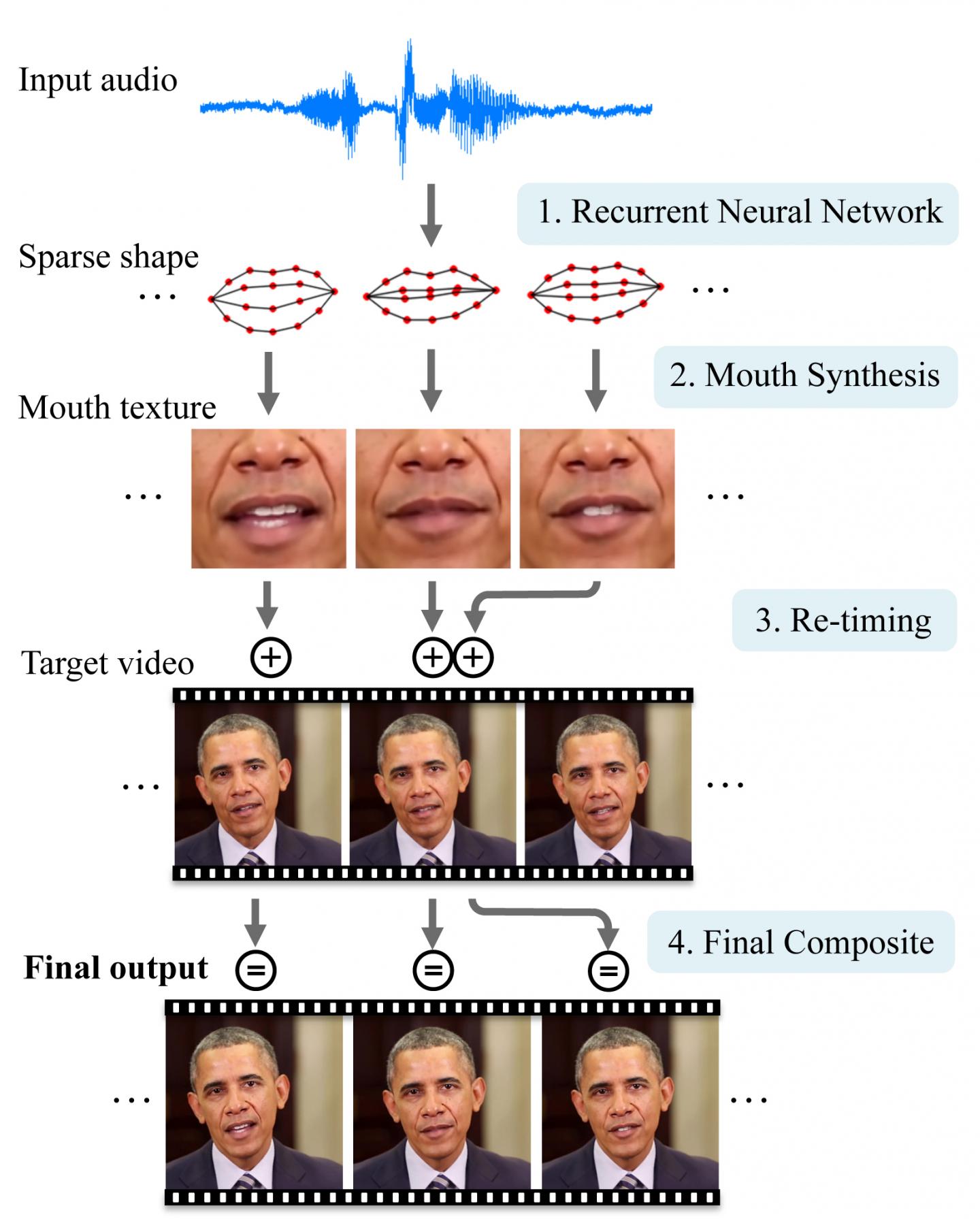
A neural network first converts the sounds from an audio file into basic mouth shapes. Then the system grafts and blends those mouth shapes onto an existing target video and adjusts the timing to create a realistic, lip-synced video of the person delivering the new speech. (credit: University of Washington)

1. Find or record a video of the person (or use video chat tools like Skype to create a new video) for the neural network to learn from. There are millions of hours of video that already exist from interviews, video chats, movies, television programs and other sources, the researchers note. (Obama was chosen because there were hours of presidential videos in the public domain.)

2. Train the neural network to watch videos of the person and translate different audio sounds into basic mouth shapes.

3. The system then uses the audio of an individual’s speech to generate realistic mouth shapes, which are then grafted onto and blended with the head of that person. Use a small time shift to enable the neural network to anticipate what the person is going to say next.

4. Currently, the neural network is designed to learn on one individual at a time, meaning that Obama’s voice — speaking words he actually uttered — is the only information used to “drive” the synthesized video. Future steps, however, include helping the algorithms generalize across situations to recognize a person’s voice and speech patterns with less data, with only an hour of video to learn from, for instance, instead of 14 hours.

Fakes of fakes

So the obvious question is: Can you use someone else’s voice on a video (assuming enough videos)? The researchers said they decided against going down the path, but they didn’t say it was impossible.

Even more pernicious: the original video person’s words (not just the voice) could be faked using Princeton/Adobe’s “VoCo” software (when available) — simply by editing a text transcript of their voice recording — or the fake voice itself could be modified.

Or Disney Research’s FaceDirector could be used to edit recorded substitute facial expressions (along with the fake voice) into the video.

However, by reversing the process — feeding video into the neural network instead of just audio — one could also potentially develop algorithms that could detect whether a video is real or manufactured, the researchers note.

The research was funded by Samsung, Google, Facebook, Intel, and the UW Animation Research Labs. You can contact the research team at audiolipsync@cs.washington.edu.


Abstract of Synthesizing Obama: Learning Lip Sync from Audio

Given audio of President Barack Obama, we synthesize a high quality video of him speaking with accurate lip sync, composited into a target video clip. Trained on many hours of his weekly address footage, a recurrent neural network learns the mapping from raw audio features to mouth shapes. Given the mouth shape at each time instant, we synthesize high quality mouth texture, and composite it with proper 3D pose matching to change what he appears to be saying in a target video to match the input audio track. Our approach produces photorealistic results.

How to ‘talk’ to your computer or car with hand or body poses

Researchers at Carnegie Mellon University’s Robotics Institute have developed a system that can detect and understand body poses and movements of multiple people from a video in real time — including, for the first time, the pose of each individual’s fingers.

The ability to recognize finger or hand poses, for instance, will make it possible for people to interact with computers in new and more natural ways, such as simply pointing at things.

That will also allow robots to perceive you’re doing, what moods you’re in, and whether you can be interrupted, for example. Your self-driving car could get an early warning that a pedestrian is about to step into the street by monitoring your body language. The technology could also be used for behavioral diagnosis and rehabilitation for conditions such as autism, dyslexia, and depression, the researchers say.

This new method was developed at CMU’s NSF-funded Panoptic Studio, a two-story dome embedded with 500 video cameras, but the researchers can now do the same thing with a single camera and laptop computer.

The researchers have released their computer code. It’s already being widely used by research groups, and more than 20 commercial groups, including automotive companies, have expressed interest in licensing the technology, according to Yaser Sheikh, associate professor of robotics.

Tracking multiple people in real time, particularly in social situations where they may be in contact with each other, presents a number of challenges. Sheikh and his colleagues took a bottom-up approach, which first localizes all the body parts in a scene — arms, legs, faces, etc. — and then associates those parts with particular individuals.

Sheikh and his colleagues will present reports on their multiperson and hand-pose detection methods at CVPR 2017, the Computer Vision and Pattern Recognition Conference, July 21–26 in Honolulu.

Radical new vertically integrated 3D chip design combines computing and data storage

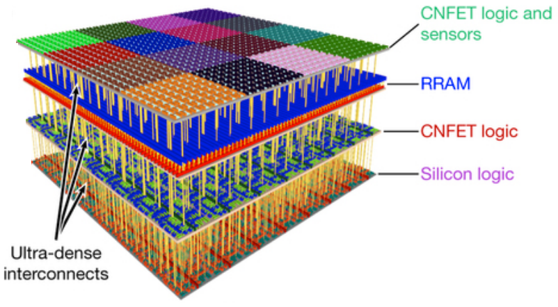
Four vertical layers in new 3D nanosystem chip. Top (fourth layer): sensors and more than one million carbon-nanotube field-effect transistor (CNFET) logic inverters; third layer, on-chip non-volatile RRAM (1 Mbit memory); second layer, CNFET logic with classification accelerator (to identify sensor inputs); first (bottom) layer, silicon FET logic. (credit: Max M. Shulaker et al./Nature)

A radical new 3D chip that combines computation and data storage in vertically stacked layers — allowing for processing and storing massive amounts of data at high speed in future transformative nanosystems — has been designed by researchers at Stanford University and MIT.

The new 3D-chip design* replaces silicon with carbon nanotubes (sheets of 2-D graphene formed into nanocylinders) and integrates resistive random-access memory (RRAM) cells.

Carbon-nanotube field-effect transistors (CNFETs) are an emerging transistor technology that can scale beyond the limits of silicon MOSFETs (conventional chips), and promise an order-of-magnitude improvement in energy-efficient computation. However, experimental demonstrations of CNFETs so far have been small-scale and limited to integrating only tens or hundreds of devices (see earlier 2015 Stanford research, “Skyscraper-style carbon-nanotube chip design…”).

The researchers integrated more than 1 million RRAM cells and 2 million carbon-nanotube field-effect transistors in the chip, making it the most complex nanoelectronic system ever made with emerging nanotechnologies, according to the researchers. RRAM is an emerging memory technology that promises high-capacity, non-volatile data storage, with improved speed, energy efficiency, and density, compared to dynamic random-access memory (DRAM).

Instead of requiring separate components, the RRAM cells and carbon nanotubes are built vertically over one another, creating a dense new 3D computer architecture** with interleaving layers of logic and memory. By using ultradense through-chip vias (electrical interconnecting wires passing between layers), the high delay with conventional wiring between computer components is eliminated.

The new 3D nanosystem can capture massive amounts of data every second, store it directly on-chip, perform in situ processing of the captured data, and produce “highly processed” information. “Such complex nanoelectronic systems will be essential for future high-performance, highly energy-efficient electronic systems,” the researchers say.

How to combine computation and storage

Illustration of separate CPU (bottom) and RAM memory (top) in current computer architecture (images credit: iStock)

The new chip design aims to replace current chip designs, which separate computing and data storage, resulting in limited-speed connections.

Separate 2D chips have been required because “building conventional silicon transistors involves extremely high temperatures of over 1,000 degrees Celsius,” explains lead author Max Shulaker, an assistant professor of electrical engineering and computer science at MIT and lead author of a paper published July 5, 2017 in the journal Nature. “If you then build a second layer of silicon circuits on top, that high temperature will damage the bottom layer of circuits.”

Instead, carbon nanotube circuits and RRAM memory can be fabricated at much lower temperatures: below 200 C. “This means they can be built up in layers without harming the circuits beneath,” says Shulaker.

Overcoming communication and computing bottlenecks

As applications analyze increasingly massive volumes of data, the limited rate at which data can be moved between different chips is creating a critical communication “bottleneck.” And with limited real estate on increasingly miniaturized chips, there is not enough room to place chips side-by-side.

At the same time, embedded intelligence in areas ranging from autonomous driving to personalized medicine is now generating huge amounts of data, but silicon transistors are no longer improving at the historic rate that they have for decades.

Instead, three-dimensional integration is the most promising approach to continue the technology-scaling path set forth by Moore’s law, allowing an increasing number of devices to be integrated per unit volume, according to Jan Rabaey, a professor of electrical engineering and computer science at the University of California at Berkeley, who was not involved in the research.

Three-dimensional integration “leads to a fundamentally different perspective on computing architectures, enabling an intimate interweaving of memory and logic,” he says. “These structures may be particularly suited for alternative learning-based computational paradigms such as brain-inspired systems and deep neural nets, and the approach presented by the authors is definitely a great first step in that direction.”

The new 3D design provides several benefits for future computing systems, including:

  • Logic circuits made from carbon nanotubes can be an order of magnitude more energy-efficient compared to today’s logic made from silicon.
  • RRAM memory is denser, faster, and more energy-efficient compared to conventional DRAM (dynamic random-access memory) devices.
  • The dense through-chip vias (wires) can enable vertical connectivity that is 1,000 times more dense than conventional packaging and chip-stacking solutions allow, which greatly improves the data communication bandwidth between vertically stacked functional layers. For example, each sensor in the top layer can connect directly to its respective underlying memory cell with an inter-layer via. This enables the sensors to write their data in parallel directly into memory and at high speed.
  • The design is compatible in both fabrication and design with today’s CMOS silicon infrastructure.

Shulaker next plans to work with Massachusetts-based semiconductor company Analog Devices to develop new versions of the system.

This work was funded by the Defense Advanced Research Projects Agency, the National Science Foundation, Semiconductor Research Corporation, STARnet SONIC, and member companies of the Stanford SystemX Alliance.

* As a working-prototype demonstration of the potential of the technology, the researchers took advantage of the ability of carbon nanotubes to also act as sensors. On the top layer of the chip, they placed more than 1 million carbon nanotube-based sensors, which they used to detect and classify ambient gases for detecting signs of disease by sensing particular compounds in a patient’s breath, says Shulaker. By layering sensing, data storage, and computing, the chip was able to measure each of the sensors in parallel, and then write directly into its memory, generating huge bandwidth in just one device, according to Shulaker. The top layer could be replaced with additional computation or data storage subsystems, or with other forms of input/output, he explains.

** Previous R&D in 3D chip technologies and their limitations are covered here, noting that “in general, 3D integration is a broad term that includes such technologies as 3D wafer-level packaging (3DWLP); 2.5D and 3D interposer-based integration; 3D stacked ICs (3D-SICs), monolithic 3D ICs; 3D heterogeneous integration; and 3D systems integration.” The new Stanford-MIT nanosystem design significantly expands this definition.


Abstract of Three-dimensional integration of nanotechnologies for computing and data storage on a single chip

The computing demands of future data-intensive applications will greatly exceed the capabilities of current electronics, and are unlikely to be met by isolated improvements in transistors, data storage technologies or integrated circuit architectures alone. Instead, transformative nanosystems, which use new nanotechnologies to simultaneously realize improved devices and new integrated circuit architectures, are required. Here we present a prototype of such a transformative nanosystem. It consists of more than one million resistive random-access memory cells and more than two million carbon-nanotube field-effect transistors—promising new nanotechnologies for use in energy-efficient digital logic circuits and for dense data storage—fabricated on vertically stacked layers in a single chip. Unlike conventional integrated circuit architectures, the layered fabrication realizes a three-dimensional integrated circuit architecture with fine-grained and dense vertical connectivity between layers of computing, data storage, and input and output (in this instance, sensing). As a result, our nanosystem can capture massive amounts of data every second, store it directly on-chip, perform in situ processing of the captured data, and produce ‘highly processed’ information. As a working prototype, our nanosystem senses and classifies ambient gases. Furthermore, because the layers are fabricated on top of silicon logic circuitry, our nanosystem is compatible with existing infrastructure for silicon-based technologies. Such complex nano-electronic systems will be essential for future high-performance and highly energy-efficient electronic systems.

Smart algorithm automatically adjusts exoskeletons for best walking performance

Walk this way: Metabolic feedback and optimization algorithm automatically tweaks exoskeleton for optimal performance. (credit: Kirby Witte, Katie Poggensee, Pieter Fiers, Patrick Franks & Steve Collins)

Researchers at the College of Engineering at Carnegie Mellon University (CMU) have developed a new automated feedback system for personalizing exoskeletons to achieve optimal performance.

Exoskeletons can be used to augment human abilities. For example, they can provide more endurance while walking, help lift a heavy load, improve athletic performance, and help a stroke patient walk again.

But current one-size-fits-all exoskeleton devices, despite their potential, “have not improved walking performance as much as we think they should,” said Steven Collins, a professor of Mechanical Engineering and senior author of a paper published published Friday June 23, 2017 in Science.

The problem: An exoskeleton needs to be adjusted (and re-adjusted) to work effectively for each user — currently, a time-consuming, iffy manual process.

So the CMU engineers developed a more effective “human-in-the-loop optimization” technique that measures the amount of energy the walker expends by monitoring their breathing* — automatically adjusting the exoskeleton’s ankle dynamics to minimize required human energy expenditure.**

Using real-time metabolic cost estimation for each individual, the CMU software algorithm, combined with versatile emulator hardware, optimized the exoskeleton torque pattern for one ankle while walking, running, and carrying a load on a treadmill. The algorithm automatically made optimized adjustments for each pattern, based on measurements of a person’s energy use for 32 different walking patterns over the course of an hour. (credit: Juanjuan Zhang et al./Science, adapted by KurzweilAI)

In a lab study with 11 healthy volunteers, the new technique resulted in an average reduction in effort of 24% compared to participants walking with the exoskeleton powered off. The technique yielded higher user benefits than in any exoskeleton study to date, including devices acting at all joints on both legs, according to the researchers.

* “In daily life, a proxy measure such as heart rate or muscle activity could be used for optimization, providing noisier but more abundant performance data.” — Juanjuan Zhang et al./Science

** Ankle torque in the lab study was determined by four parameters: peak torque, timing of peak torque, and rise and fall times. This method was chosen to allow comparisons to a prior study that used the same hardware.


Science/AAAS | Personalized Exoskeletons Are Taking Support One Step Farther


Abstract of Human-in-the-loop optimization of exoskeleton assistance during walking

Exoskeletons and active prostheses promise to enhance human mobility, but few have succeeded. Optimizing device characteristics on the basis of measured human performance could lead to improved designs. We have developed a method for identifying the exoskeleton assistance that minimizes human energy cost during walking. Optimized torque patterns from an exoskeleton worn on one ankle reduced metabolic energy consumption by 24.2 ± 7.4% compared to no torque. The approach was effective with exoskeletons worn on one or both ankles, during a variety of walking conditions, during running, and when optimizing muscle activity. Finding a good generic assistance pattern, customizing it to individual needs, and helping users learn to take advantage of the device all contributed to improved economy. Optimization methods with these features can substantially improve performance.

Two drones see through walls in 3D using WiFi signals

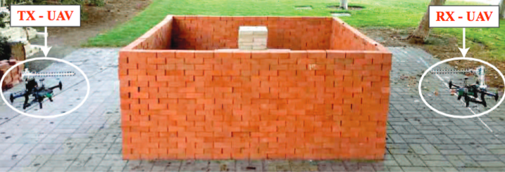
Transmit and receive drones perform 3D imaging through walls using WiFi (credit: Chitra R. Karanam and Yasamin Mostofi/ACM)

Researchers at the University of California Santa Barbara have demonstrated the first three-dimensional imaging of objects through walls using an ordinary wireless signal.

Applications could include emergency search-and-rescue, archaeological discovery, and structural monitoring, according to the researchers. Other applications could include military and law-enforcement surveillance.

Calculating 3D images from WiFi signals

In the research, two octo-copters (drones) took off and flew outside an enclosed, four-sided brick structure whose interior was unknown to the drones. One drone continuously transmitted a WiFi signal; the other drone (located on a different side of the structure) received that signal and transmitted the changes in received signal strength (“RSSI”) during the flight to a computer, which then calculated 3D high-resolution images of the objects inside (which do not need to move).

Structure and resulting 3D image (credit: Chitra R. Karanam and Yasamin Mostofi/ACM)

Interestingly, the equipment is all commercially available: two drones with “yagi” antenna, WiFi router, Tango tablet (for real-time localization), and Raspberry Pi computer with network interface to record measurements.

This development builds on previous 2D work by professor Yasamin Mostofi’s lab, which has pioneered sensing and imaging with everyday radio frequency signals such as WiFi. Mostofi says the success of the 3D experiments is due to the drones’ ability to approach the area from several angles, and to new methodology* developed by her lab.

The research is described in an open-access paper published April 2017 in proceedings of the Association for Computing Machinery/Institute of Electrical and Electronics Engineers International Conference on Information Processing in Sensor Networks (IPSN).

A later paper by Technical University of Munich physicists also reported a system intended for 3D imaging with WiFi, but with only simulated (and cruder) images. (An earlier 2009 paper by Mostofi et al. also reported simulated results for 3D see-through imaging of structures.)

Block diagram of the 3D through-wall imaging system (credit: Chitra R. Karanam and Yasamin Mostofi/ACM)

* The researchers’ approach to enabling 3D through-wall imaging utilizes four tightly integrated key components, according to the paper.

(1) They proposed robotic paths that can capture the spatial variations in all three dimensions as much as possible, while maintaining the efficiency of the operation. 

(2) They modeled the three-dimensional unknown area of interest as a Markov Random Field to capture the spatial dependencies, and utilized a graph-based belief propagation approach to update the imaging decision of each voxel (the smallest unit of a 3D image) based on the decisions of the neighboring voxels. 

(3) To approximate the interaction of the transmitted wave with the area of interest, they used a linear wave model.

(4) They took advantage of the compressibility of the information content to image the area with a very small number of WiFi measurements (less than 4 percent).


Mostofi Lab | X-ray Eyes in the Sky: Drones and WiFi for 3D Through-Wall Imaging


Abstract of 3D Through-Wall Imaging with Unmanned Aerial Vehicles Using WiFi

In this paper, we are interested in the 3D through-wall imaging of a completely unknown area, using WiFi RSSI and Unmanned Aerial Vehicles (UAVs) that move outside of the area of interest to collect WiFi measurements. It is challenging to estimate a volume represented by an extremely high number of voxels with a small number of measurements. Yet many applications are time-critical and/or limited on resources, precluding extensive measurement collection. In this paper, we then propose an approach based on Markov random field modeling, loopy belief propagation, and sparse signal processing for 3D imaging based on wireless power measurements. Furthermore, we show how to design ecient aerial routes that are informative for 3D imaging. Finally, we design and implement a complete experimental testbed and show high-quality 3D robotic through-wall imaging of unknown areas with less than 4% of measurements.

Crystal ‘domain walls’ may lead to tinier electronic devices

Abstract art? No, nanoscale crystal sheets with moveable conductive “domain walls” that can modify a circuit’s electronic properties (credit: Queen’s University Belfast)

Queen’s University Belfast physicists have discovered a radical new way to modify the conductivity (ease of electron flow) of electronic circuits — reducing the size of future devices.

The two latest KurzweilAI articles on graphene cited faster/lower-power performance and device-compatibility features. This new research takes another approach: Altering the properties of a crystal to eliminate the need for multiple circuits in devices.

Reconfigurable nanocircuitry

To do that, the scientists used “ferroelectric copper-chlorine boracite” crystal sheets, which are almost as thin as graphene. The researchers discovered that squeezing the crystal sheets with a sharp needle at a precise location causes a jigsaw-puzzle-like pattern of “domains walls” to develop around the contact point.

Then, using external applied electric fields, these writable, erasable domain walls can be repeatedly moved around in the crystal to create a variety of new electronic properties. They can appear, disappear, or move around within the crystal, all without permanently altering the crystal itself.

Eliminating the need for multiple circuits may reduce the size of future computers and other devices, according to the researchers.

The team’s findings have been published in an open-access paper in Nature Communications.


Abstract of Injection and controlled motion of conducting domain walls in improper ferroelectric Cu-Cl boracite

Ferroelectric domain walls constitute a completely new class of sheet-like functional material. Moreover, since domain walls are generally writable, erasable and mobile, they could be useful in functionally agile devices: for example, creating and moving conducting walls could make or break electrical connections in new forms of reconfigurable nanocircuitry. However, significant challenges exist: site-specific injection and annihilation of planar walls, which show robust conductivity, has not been easy to achieve. Here, we report the observation, mechanical writing and controlled movement of charged conducting domain walls in the improper-ferroelectric Cu3B7O13Cl. Walls are straight, tens of microns long and exist as a consequence of elastic compatibility conditions between specific domain pairs. We show that site-specific injection of conducting walls of up to hundreds of microns in length can be achieved through locally applied point-stress and, once created, that they can be moved and repositioned using applied electric fields.

New chemical method could revolutionize graphene use in electronics

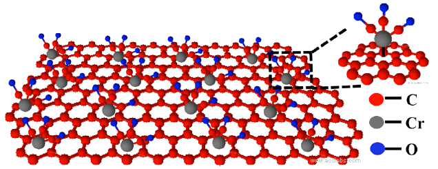
Adding a molecular structure containing carbon, chromium, and oxygen atoms retains graphene’s superior conductive properties. The metal atoms (silver, in this experiment) to be bonded are then added to the oxygen atoms on top. (credit: Songwei Che et al./Nano Letters)

University of Illinois at Chicago scientists have solved a fundamental problem that has held back the use of wonder material graphene in a wide variety of electronics applications.

When graphene is bonded (attached) to metal atoms (such as molybdenum) in devices such as solar cells, graphene’s superior conduction properties degrade.

The solution: Instead of adding molecules directly to the individual carbon atoms of graphene, the new method first adds a sort of buffer (consisting of chromium, carbon, and oxygen atoms) to the graphene, and then adds the metal atoms to this buffer material instead. That enables the graphene to retain its unique properties of electrical conduction.

In an experiment, the researchers successfully added silver nanoparticles to graphene with this method. That increased the material’s ability to boost the efficiency of graphene-based solar cells by 11 fold, said Vikas Berry, associate professor and department head of chemical engineering and senior author of a paper on the research, published in Nano Letters.

Researchers at Indian Institute of Technology and Clemson University were also involved in the study. The research was funded by the National Science Foundation.


Abstract of Retained Carrier-Mobility and Enhanced Plasmonic-Photovoltaics of Graphene via ring-centered η6 Functionalization and Nanointerfacing

Binding graphene with auxiliary nanoparticles for plasmonics, photovoltaics, and/or optoelectronics, while retaining the trigonal-planar bonding of sp2 hybridized carbons to maintain its carrier-mobility, has remained a challenge. The conventional nanoparticle-incorporation route for graphene is to create nucleation/attachment sites via “carbon-centered” covalent functionalization, which changes the local hybridization of carbon atoms from trigonal-planar sp2to tetrahedral sp3. This disrupts the lattice planarity of graphene, thus dramatically deteriorating its mobility and innate superior properties. Here, we show large-area, vapor-phase, “ring-centered” hexahapto (η6) functionalization of graphene to create nucleation-sites for silver nanoparticles (AgNPs) without disrupting its sp2 character. This is achieved by the grafting of chromium tricarbonyl [Cr(CO)3] with all six carbon atoms (sigma-bonding) in the benzenoid ring on graphene to form an (η6-graphene)Cr(CO)3 complex. This nondestructive functionalization preserves the lattice continuum with a retention in charge carrier mobility (9% increase at 10 K); with AgNPs attached on graphene/n-Si solar cells, we report an ∼11-fold plasmonic-enhancement in the power conversion efficiency (1.24%).

Graphene-based computer would be 1,000 times faster than silicon-based, use 100th the power

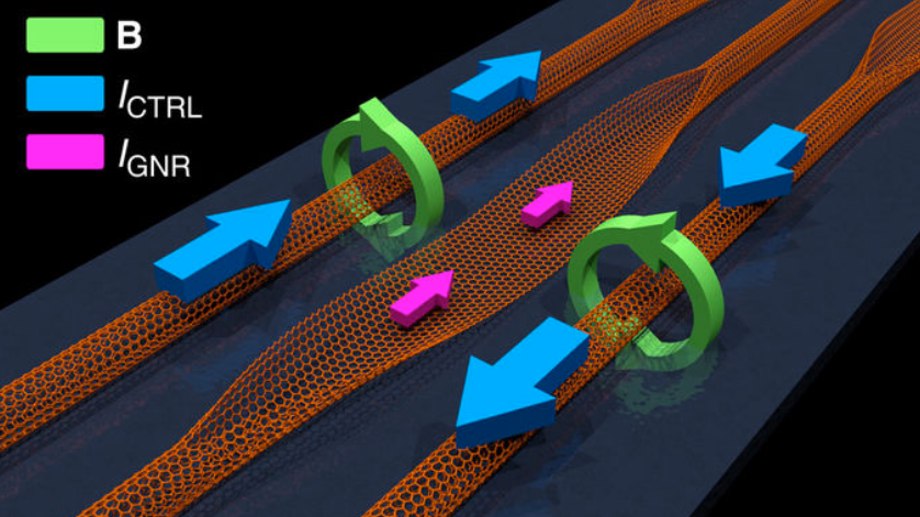
How a graphene-based transistor would work. A graphene nanoribbon (GNR) is created by unzipping (opening up) a portion of a carbon nanotube (CNT) (the flat area, shown with pink arrows above it). The GRN switching is controlled by two surrounding parallel CNTs. The magnitudes and relative directions of the control current, ICTRL (blue arrows) in the CNTs determine the rotation direction of the magnetic fields, B (green). The magnetic fields then control the GNR magnetization (based on the recent discovery of negative magnetoresistance), which causes the GNR to switch from resistive (no current) to conductive, resulting in current flow, IGNR (pink arrows) — in other words, causing the GNR to act as a transistor gate. The magnitude of the current flow through the GNR functions as the binary gate output — with binary 1 representing the current flow of the conductive state and binary 0 representing no current (the resistive state). (credit: Joseph S. Friedman et al./Nature Communications)

A future graphene-based transistor using spintronics could lead to tinier computers that are a thousand times faster and use a hundredth of the power of silicon-based computers.

The radical transistor concept, created by a team of researchers at Northwestern University, The University of Texas at Dallas, University of Illinois at Urbana-Champaign, and University of Central Florida, is explained this month in an open-access paper in the journal Nature Communications.

Transistors act as on and off switches. A series of transistors in different arrangements act as logic gates, allowing microprocessors to solve complex arithmetic and logic problems. But the speed of computer microprocessors that rely on silicon transistors has been relatively stagnant since around 2005, with clock speeds mostly in the 3 to 4 gigahertz range.

Clock speeds approaching the terahertz range

The researchers discovered that by applying a magnetic field to a graphene ribbon (created by unzipping a carbon nanotube), they could change the resistance of current flowing through the ribbon. The magnetic field — controlled by increasing or decreasing the current through adjacent carbon nanotubes — increased or decreased the flow of current.

A cascading series of graphene transistor-based logic circuits could produce a massive jump, with clock speeds approaching the terahertz range — a thousand times faster.* They would also be smaller and substantially more efficient, allowing device-makers to shrink technology and squeeze in more functionality, according to Ryan M. Gelfand, an assistant professor in The College of Optics & Photonics at the University of Central Florida.

The researchers hope to inspire the fabrication of these cascaded logic circuits to stimulate a future transformative generation of energy-efficient computing.

* Unlike other spintronic logic proposals, these new logic gates can be cascaded directly through the carbon materials without requiring intermediate circuits and amplification between gates. That would result in compact circuits with reduced area that are far more efficient than with CMOS switching, which is limited by charge transfer and accumulation from RLC (resistance-inductance-capacitance) interconnect delays.


Abstract of Cascaded spintronic logic with low-dimensional carbon

Remarkable breakthroughs have established the functionality of graphene and carbon nanotube transistors as replacements to silicon in conventional computing structures, and numerous spintronic logic gates have been presented. However, an efficient cascaded logic structure that exploits electron spin has not yet been demonstrated. In this work, we introduce and analyse a cascaded spintronic computing system composed solely of low-dimensional carbon materials. We propose a spintronic switch based on the recent discovery of negative magnetoresistance in graphene nanoribbons, and demonstrate its feasibility through tight-binding calculations of the band structure. Covalently connected carbon nanotubes create magnetic fields through graphene nanoribbons, cascading logic gates through incoherent spintronic switching. The exceptional material properties of carbon materials permit Terahertz operation and two orders of magnitude decrease in power-delay product compared to cutting-edge microprocessors. We hope to inspire the fabrication of these cascaded logic circuits to stimulate a transformative generation of energy-efficient computing.

High-speed light-based systems could replace supercomputers for certain ‘deep learning’ calculations

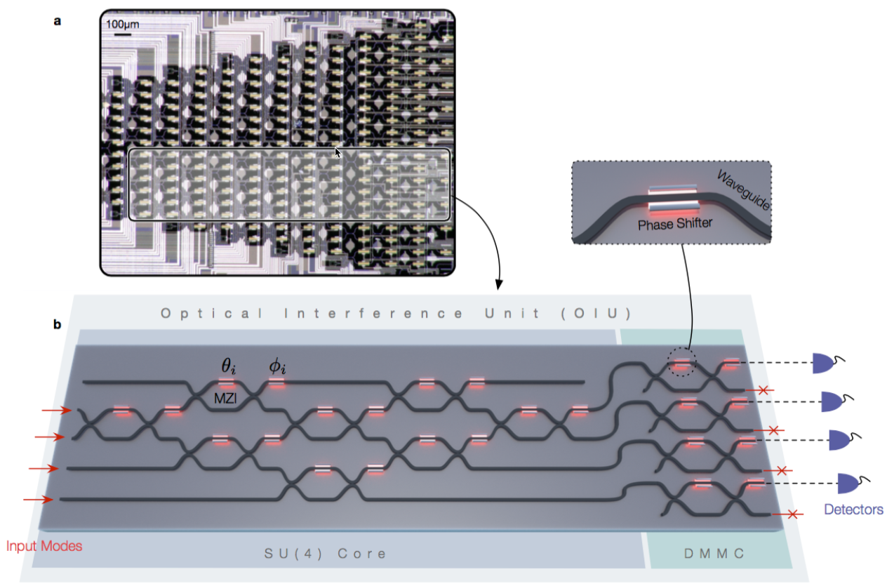
(a) Optical micrograph of an experimentally fabricated on-chip optical interference unit; the physical region where the optical neural network program exists is highlighted in gray. A programmable nanophotonic processor uses a field-programmable gate array (similar to an FPGA integrated circuit ) — an array of interconnected waveguides, allowing the light beams to be modified as needed for a specific deep-learning matrix computation. (b) Schematic illustration of the optical neural network program, which performs matrix multiplication and amplification fully optically. (credit: Yichen Shen et al./Nature Photonics)

A team of researchers at MIT and elsewhere has developed a new approach to deep learning systems — using light instead of electricity, which they say could vastly improve the speed and efficiency of certain deep-learning computations.

Deep-learning systems are based on artificial neural networks that mimic the way the brain learns from an accumulation of examples. They can enable technologies such as face- and voice-recognition software, or scour vast amounts of medical data to find patterns that could be useful diagnostically, for example.

But the computations these systems carry out are highly complex and demanding, even for supercomputers. Traditional computer architectures are not very efficient for calculations needed for neural-network tasks that involve repeated multiplications of matrices (arrays of numbers). These can be computationally intensive for conventional CPUs or even GPUs.

Programmable nanophotonic processor

Instead, the new approach uses an optical device that the researchers call a “programmable nanophotonic processor.” Multiple light beams are directed in such a way that their waves interact with each other, producing interference patterns that “compute” the intended operation.

The optical chips using this architecture could, in principle, carry out dense matrix multiplications (the most power-hungry and time-consuming part in AI algorithms) for learning tasks much faster, compared to conventional electronic chips. The researchers expect a computational speed enhancement of at least two orders of magnitude over the state-of-the-art and three orders of magnitude in power efficiency.

“This chip, once you tune it, can carry out matrix multiplication with, in principle, zero energy, almost instantly,” says Marin Soljacic, one of the MIT researchers on the team.

To demonstrate the concept, the team set the programmable nanophotonic processor to implement a neural network that recognizes four basic vowel sounds. Even with the prototype system, they were able to achieve a 77 percent accuracy level, compared to about 90 percent for conventional systems. There are “no substantial obstacles” to scaling up the system for greater accuracy, according to Soljacic.

The team says is will still take a lot more time and effort to make this system useful. However, once the system is scaled up and fully functioning, the low-power system should find many uses, especially for situations where power is limited, such as in self-driving cars, drones, and mobile consumer devices. Other uses include signal processing for data transmission and computer centers.

The research was published Monday (June 12, 2017) in a paper in the journal Nature Photonics (open-access version available on arXiv).

The team also included researchers at Elenion Technologies of New York and the Université de Sherbrooke in Quebec. The work was supported by the U.S. Army Research Office through the Institute for Soldier Nanotechnologies, the National Science Foundation, and the Air Force Office of Scientific Research.


Abstract of Deep learning with coherent nanophotonic circuits

Artificial neural networks are computational network models inspired by signal processing in the brain. These models have dramatically improved performance for many machine-learning tasks, including speech and image recognition. However, today’s computing hardware is inefficient at implementing neural networks, in large part because much of it was designed for von Neumann computing schemes. Significant effort has been made towards developing electronic architectures tuned to implement artificial neural networks that exhibit improved computational speed and accuracy. Here, we propose a new architecture for a fully optical neural network that, in principle, could offer an enhancement in computational speed and power efficiency over state-of-the-art electronics for conventional inference tasks. We experimentally demonstrate the essential part of the concept using a programmable nanophotonic processor featuring a cascaded array of 56 programmable Mach–Zehnder interferometers in a silicon photonic integrated circuit and show its utility for vowel recognition.

A noninvasive method for deep-brain stimulation for brain disorders

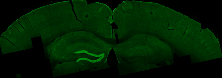
External electrical waves excite an area in the mouse hippocampus, shown in bright green. (credit: Nir Grossman, Ph.D., Suhasa B. Kodandaramaiah, Ph.D., and Andrii Rudenko, Ph.D.)

MIT researchers and associates have come up with a breakthrough method of remotely stimulating regions deep within the brain, replacing the invasive surgery now required for implanting electrodes for Parkinson’s and other brain disorders.

The new method could make deep-brain stimulation for brain disorders less expensive, more accessible to patients, and less risky (avoiding brain hemorrhage and infection).

Working with mice, the researchers applied two high-frequency electrical currents at two slightly different frequencies (E1 and E2 in the diagram below), attaching electrodes (similar those used with an EEG brain machine) to the surface of the skull.

A new noninvasive method for deep-brain stimulation (credit: Grossman et al./Cell)

At these higher brain frequencies, the currents have no effect on brain tissues. But where the currents converge deep in the brain, they interfere with one another in such a way that they generate low-frequency current (corresponding to the red envelope in the diagram) inside neurons, thus stimulating neural electrical activity.

The researchers named this method “temporal interference stimulation” (that is, interference between pulses in the two currents at two slightly different times — generating the difference frequency).* For the experimental setup shown in the diagram above, the E1 current was 1kHz (1,000 Hz), which mixed with a 1.04kHz E2 current. That generated a current with a 40Hz “delta f” difference frequency — a frequency that can stimulate neural activity in the brain. (The researchers found no harmful effects in any part of the mouse brain.)

“Traditional deep-brain stimulation requires opening the skull and implanting an electrode, which can have complications,” explains Ed Boyden, an associate professor of biological engineering and brain and cognitive sciences at MIT, and the senior author of the study, which appears in the June 1, 2017 issue of the journal Cell. Also, “only a small number of people can do this kind of neurosurgery.”

Custom-designed, targeted deep-brain stimulation

If this new method is perfected and clinically tested, neurologists could control the size and location of the exact tissue that receives the electrical stimulation for each patient, by selecting the frequency of the currents and the number and location of the electrodes, according to the researchers.

Neurologists could also steer the location of deep-brain stimulation in real time, without moving the electrodes, by simply altering the currents. In this way, deep targets could be stimulated for conditions such as Parkinson’s, epilepsy, depression, and obsessive-compulsive disorder — without affecting surrounding brain structures.

The researchers are also exploring the possibility of using this method to experimentally treat other brain conditions, such as autism, and for basic science investigations.

Co-author Li-Huei Tsai, director of MIT’s Picower Institute for Learning and Memory, and researchers in her lab tested this technique in mice and found that they could stimulate small regions deep within the brain, including the hippocampus. But they were also able to shift the site of stimulation, allowing them to activate different parts of the motor cortex and prompt the mice to move their limbs, ears, or whiskers.

“We showed that we can very precisely target a brain region to elicit not just neuronal activation but behavioral responses,” says Tsai.

Last year, Tsai showed (open access) that using light to visually induce brain waves of a particular frequency could substantially reduce the beta amyloid plaques seen in Alzheimer’s disease, in the brains of mice. She now plans to explore whether this new type of electrical stimulation could offer a new way to generate the same type of beneficial brain waves.

This new method is also an alternative to other brain-stimulation methods.

Transcranial magnetic stimulation (TMS), which is FDA-approved for treating depression and to study the basic science of cognition, emotion, sensation, and movement, can stimulate deep brain structures but can result in surface regions being strongly stimulated, according to the researchers.

Transcranial ultrasound and expression of heat-sensitive receptors and injection of thermomagnetic nanoparticles have been proposed, “but the unknown mechanism of action … and the need to genetically manipulate the brain, respectively, may limit their immediate use in humans,” the researchers note in the paper.

The MIT researchers collaborated with investigators at Beth Israel Deaconess Medical Center (BIDMC), the IT’IS Foundation, Harvard Medical School, and ETH Zurich.

The research was funded in part by the Wellcome Trust, a National Institutes of Health Director’s Pioneer Award, an NIH Director’s Transformative Research Award, the New York Stem Cell Foundation Robertson Investigator Award, the MIT Center for Brains, Minds, and Machines, Jeremy and Joyce Wertheimer, Google, a National Science Foundation Career Award, the MIT Synthetic Intelligence Project, and Harvard Catalyst: The Harvard Clinical and Translational Science Center.

* Similar to a radio-frequency or audio “beat frequency.”


Abstract of Noninvasive Deep Brain Stimulation via Temporally Interfering Electric Fields

We report a noninvasive strategy for electrically stimulating neurons at depth. By delivering to the brain multiple electric fields at frequencies too high to recruit neural firing, but which differ by a frequency within the dynamic range of neural firing, we can electrically stimulate neurons throughout a region where interference between the multiple fields results in a prominent electric field envelope modulated at the difference frequency. We validated this temporal interference (TI) concept via modeling and physics experiments, and verified that neurons in the living mouse brain could follow the electric field envelope. We demonstrate the utility of TI stimulation by stimulating neurons in the hippocampus of living mice without recruiting neurons of the overlying cortex. Finally, we show that by altering the currents delivered to a set of immobile electrodes, we can steerably evoke different motor patterns in living mice.