How to design and build your own robot

Two robots — robot calligrapher and puppy — produced using an interactive display tool and selecting off-the-shelf components and 3D-printed parts (credit: Carnegie Mellon University)

Carnegie Mellon University (CMU) Robotics Institute researchers have developed a simplified interactive design tool that lets you design and make your own customized legged or wheeled robot, using a mix of 3D-printed parts and off-the-shelf components.

The current process of creating new robotic systems is challenging, time-consuming, and resource-intensive. So the CMU researchers have created a visual design tool with a simple drag-and-drop interface that lets you choose from a library of standard building blocks (such as actuators and mounting brackets that are either off-the-shelf/mass-produced or can be 3D-printed) that you can combine to create complex functioning robotic systems.

(a) The design interface consists of two workspaces. The left workspace allows for designing the robot. It displays a list of various modules at the top. The leftmost menu provides various functions that allow users to define preferences for the search process visualization and for physical simulation. The right workspace (showing the robot design on a plane) runs a physics simulation of the robot for testing. (b) When you select a new module from the modules list, the system automatically makes visual suggestions (shown in red) about possible connections for this module that are relevant to the current design. (credit: Carnegie Mellon University)

An iterative design process lets you experiment by changing the number and location of actuators and adjusting the physical dimensions of your robot. An auto-completion feature can automatically generate assemblies of components by searching through possible component arrangements. It even suggests components that are compatible with each other, points out where actuators should go, and automatically generates 3D-printable structural components to connect those actuators.

Automated design process. (a) Start with a guiding mesh for the robot you want to make and select the orientations of its motors, using the drag and drop interface. (b) The system then searches for possible designs that connect a given pair of motors in user-defined locations, according to user-defined preferences. You can reject the solution and re-do the search with different preferences anytime. A proposed search solution connecting the root motor to the target motor (highlighted in dark red) is shown in light blue. Repeat this process for each pair of motors. (c) Since the legs are symmetric in this case, you would only need to use the search process for two legs. The interface lets you create the other pair of legs by simple editing operations. Finally, attach end-effectors of your choice and create a body plate to complete your awesome robot design. (d) shows the final design (with and without the guiding mesh). The dinosaur head mesh was manually added after this particular design, for aesthetic appeal. (credit: Carnegie Mellon University)

The research team, headed by Stelian Coros, CMU Robotics Institute assistant professor of robotics, designed a number of robots with the tool and verified its feasibility by fabricating two test robots (shown above) — a wheeled robot with a manipulator arm that can hold a pen for drawing, and a four-legged “puppy” robot that can walk forward or sideways. “Our work aims to make robotics more accessible to casual users,” says Coros.

Robotics Ph.D. student Ruta Desai presented a report on the design tool at the IEEE International Conference on Robotics and Automation (ICRA 2017) May 29–June 3 in Singapore. No date for the availability of this tool has been announced.

This work was supported by the National Science Foundation.


Ruta Desai | Computational Abstractions for Interactive Design of Robotic Devices (ICRA 2017)


Abstract of Computational Abstractions for Interactive Design of Robotic Devices

We present a computational design system that allows novices and experts alike to easily create custom robotic devices using modular electromechanical components. The core of our work consists of a design abstraction that models the way in which these components can be combined to form complex robotic systems. We use this abstraction to develop a visual design environment that enables an intuitive exploration of the space of robots that can be created using a given set of actuators, mounting brackets and 3d-printable components. Our computational system also provides support for design auto-completion operations, which further simplifies the task of creating robotic devices. Once robot designs are finished, they can be tested in physical simulations and iteratively improved until they meet the individual needs of their users. We demonstrate the versatility of our computational design system by creating an assortment of legged and wheeled robotic devices. To test the physical feasibility of our designs, we fabricate a wheeled device equipped with a 5-DOF arm and a quadrupedal robot.

3D-printed ‘bionic skin’ could give robots and prosthetics the sense of touch

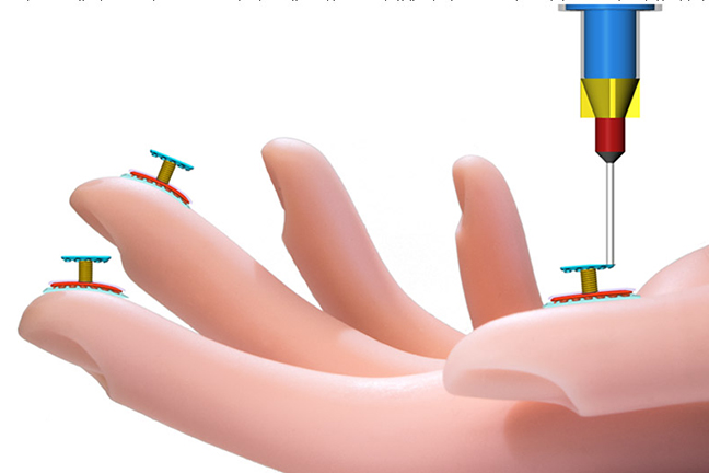
Schematic of a new kind of 3D printer that can print touch sensors directly on a model hand. (credit: Shuang-Zhuang Guo and Michael McAlpine/Advanced Materials )

Engineering researchers at the University of Minnesota have developed a process for 3D-printing stretchable, flexible, and sensitive electronic sensory devices that could give robots or prosthetic hands — or even real skin — the ability to mechanically sense their environment.

One major use would be to give surgeons the ability to feel during minimally invasive surgeries instead of using cameras, or to increase the sensitivity of surgical robots. The process could also make it easier for robots to walk and interact with their environment.

Printing electronics directly on human skin could be used for pulse monitoring, energy harvesting (of movements), detection of finger motions (on a keyboard or other devices), or chemical sensing (for example, by soldiers in the field to detect dangerous chemicals or explosives). Or imagine a future computer mouse built into your fingertip, with haptic touch on any surface.

“While we haven’t printed on human skin yet, we were able to print on the curved surface of a model hand using our technique,” said Michael McAlpine, a University of Minnesota mechanical engineering associate professor and lead researcher on the study.* “We also interfaced a printed device with the skin and were surprised that the device was so sensitive that it could detect your pulse in real time.”

The researchers also visualize use in “bionic organs.”

A unique skin-compatible 3D-printing process

(left) Schematic of the tactile sensor. (center) Top view. (right) Optical image showing the conformally printed 3D tactile sensor on a fingertip. Scale bar = 4 mm. (credit: Shuang-Zhuang Guo et al./Advanced Materials)

McAlpine and his team made the sensing fabric with a one-of-a kind 3D printer they built in the lab. The multifunctional printer has four nozzles to print the various specialized “inks” that make up the layers of the device — a base layer of silicone**, top and bottom electrodes made of a silver-based piezoresistive conducting ink, a coil-shaped pressure sensor, and a supporting layer that holds the top layer in place while it sets (later washed away in the final manufacturing process).

Surprisingly, all of the layers of “inks” used in the flexible sensors can set at room temperature. Conventional 3D printing using liquid plastic is too hot and too rigid to use on the skin. The sensors can stretch up to three times their original size.

The researchers say the next step is to move toward semiconductor inks and printing on a real surface. “The manufacturing is built right into the process, so it is ready to go now,” McAlpine said.

The research was published online in the journal Advanced Materials. It was funded by the National Institute of Biomedical Imaging and Bioengineering of the National Institutes of Health.

* McAlpine integrated electronics and novel 3D-printed nanomaterials to create a “bionic ear” in 2013.

** The silicone rubber has a low modulus of elasticity of 150 kPa, similar to that of skin, and lower hardness (Shore A 10) than that of human skin, according to the Advanced Materials paper.


College of Science and Engineering, UMN | 3D Printed Stretchable Tactile Sensors


Abstract of 3D Printed Stretchable Tactile Sensors

The development of methods for the 3D printing of multifunctional devices could impact areas ranging from wearable electronics and energy harvesting devices to smart prosthetics and human–machine interfaces. Recently, the development of stretchable electronic devices has accelerated, concomitant with advances in functional materials and fabrication processes. In particular, novel strategies have been developed to enable the intimate biointegration of wearable electronic devices with human skin in ways that bypass the mechanical and thermal restrictions of traditional microfabrication technologies. Here, a multimaterial, multiscale, and multifunctional 3D printing approach is employed to fabricate 3D tactile sensors under ambient conditions conformally onto freeform surfaces. The customized sensor is demonstrated with the capabilities of detecting and differentiating human movements, including pulse monitoring and finger motions. The custom 3D printing of functional materials and devices opens new routes for the biointegration of various sensors in wearable electronics systems, and toward advanced bionic skin applications.

Precision typing on a smartwatch with finger gestures

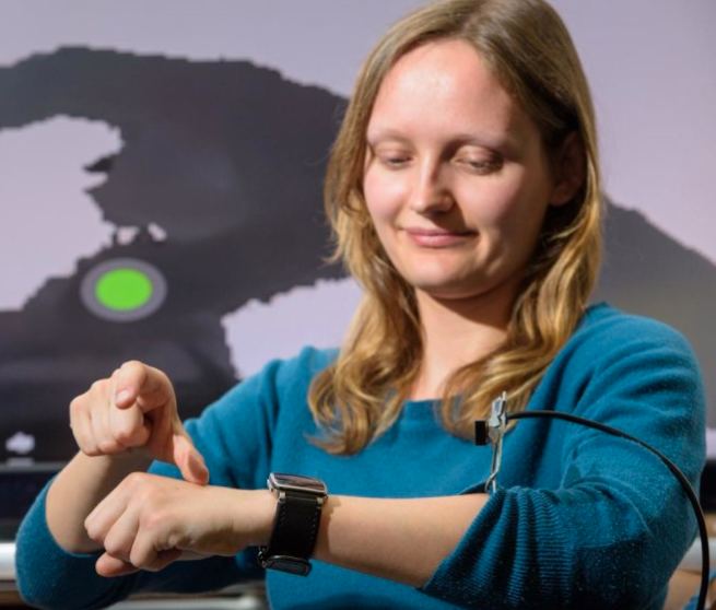
The “Watchsense” prototype uses a small depth camera attached to the arm, mimicking a depth camera on a smartwatch. It could make it easy to type, or in a music program, volume could be increased by simply raising a finger. (credit: Srinath Sridhar et al.)

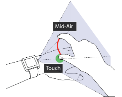
If you wear a smartwatch, you know how limiting it is to type it on or otherwise operate it. Now European researchers have developed an input method that uses a depth camera (similar to the Kinect game controller) to track fingertip touch and location on the back of the hand or in mid-air, allowing for precision control.

The researchers have created a prototype called “WatchSense,” worn on the user’s arm. It captures the movements of the thumb and index finger on the back of the hand or in the space above it. It would also work with smartphones, smart TVs, and virtual-reality or augmented reality devices, explains Srinath Sridhar, a researcher in the Graphics, Vision and Video group at the Max Planck Institute for Informatics.

KurzweilAI has covered a variety of attempts to use depth cameras for controlling devices, but developers have been plagued with the lack of precise control with current camera devices and software.

The new software, based on machine learning, recognizes the exact positions of the thumb and index finger in the 3D image from the depth sensor, says Sridhar, identifying specific fingers and dealing with the unevenness of the back of the hand and the fact that fingers can occlude each other when they are moved.

A smartwatch (or other device) could have an embedded depth sensor on its side, aimed at the back of the hand and the space above it, allowing for easy typing and control. (credit: Srinath Sridhar et al.)

“The currently available depth sensors do not fit inside a smartwatch, but from the trend it’s clear that in the near future, smaller depth sensors will be integrated into smartwatches,” Sridhar says.

The researchers, which include Christian Theobalt, head of the Graphics, Vision and Video group at MPI, Anders Markussen and Sebastian Boring at the University of Copenhagen, and Antti Oulasvirta at Aalto University in Finland, will present WatchSense at the ACM CHI Conference on Human Factors in Computing Systems in Denver (May 6–11, 2017). Their open-access paper is also available.


Srinath Sridhar et al. | WatchSense: On- and Above-Skin Input Sensing through a Wearable Depth Sensor


Abstract of WatchSense: On- and Above-Skin Input Sensing through a Wearable Depth Sensor

This paper contributes a novel sensing approach to support on- and above-skin finger input for interaction on the move. WatchSense uses a depth sensor embedded in a wearable device to expand the input space to neighboring areas of skin and the space above it. Our approach addresses challenging camera-based tracking conditions, such as oblique viewing angles and occlusions. It can accurately detect fingertips, their locations, and whether they are touching the skin or hovering above it. It extends previous work that supported either mid-air or multitouch input by simultaneously supporting both. We demonstrate feasibility with a compact, wearable prototype attached to a user’s forearm (simulating an integrated depth sensor). Our prototype—which runs in real-time on consumer mobile devices—enables a 3D input space on the back of the hand. We evaluated the accuracy and robustness of the approach in a user study. We also show how WatchSense increases the expressiveness of input by interweaving mid-air and multitouch for several interactive applications.

A ‘smart contact lens’ for diabetes and glaucoma diagnosis

Smart contact lens on mannequin eye (credit: UNIST)

Korean researchers have designed a “smart contact lens” that may one day allow patients with diabetes and glaucoma to self-monitor blood glucose levels and internal eye pressure.*

The study was conducted by researchers at Ulsan National Institute of Science and Technology (UNIST) and Kyungpook National University School of Medicine, both of South Korea.

Most previously reported contact lens sensors can only monitor a single analyte (such as glucose) at a time, and generally obstruct the field of vision of the subject.

The design is based on transparent, stretchable sensors that are deposited on commercially available soft-contact lenses.

Electrodes based on a hybrid graphene-silver nanowire material can measure glucose in tears. Internal eye pressure changes are measured by a sandwich structure whose electronic characteristics are modified by pressure.

Inductive coupling — batteries not required

Both of these readings are transmitted wirelessly using “inductive coupling” (similar to remote charging of batteries), so no connected power source, such as a battery, is required. This design also allows for 24-hour real-time monitoring by patients.

The researchers conducted in-vivo and in-vitro performance tests using a live rabbit and bovine eyeball.

The team expects that the research could also lead to developing biosensors capable of detecting and treating various other human diseases, or used as a component in other biomedical devices.

The study results were published in the March issue of the journal Nature Communications. The study was supported by the 2017 CooperVision Science and Technology (S&T) Awards Program.

* Diabetes is the most common cause of high blood sugar levels. Intraocular pressure is the largest risk factor for glaucoma, a leading cause of human blindness.


How the smart contact lens works

Schematic of the top portion of the wearable contact-lens sensor. Left: antenna. Insert: Glucose sensor, based on a field-effect transistor (FET), which consists of a graphene channel and graphene/silver nanowire for source/drain. Not shown: chromium/gold interconnect, epoxy layer, and lens (below). (credit: UNIST)

Real-time glucose sensing with graphene/silver hybrid nanostructures. For selective and sensitive detection of glucose, glucose oxidase (GOD) catalyzes oxidation of glucose to gluconic acid and reduction of water to hydrogen peroxide, which produces oxygen, protons and electrons. The concentration of charge carriers in the FET channel, and thus the drain current, increases at higher concentration of glucose. (credit: UNIST)

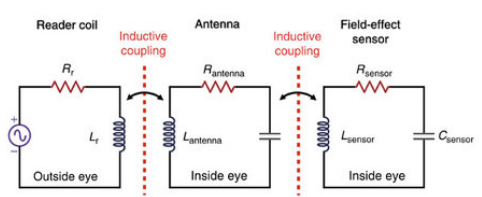
The FET sensor (right) is modeled as an electrical RLC resonant circuit, comprised of the resistance (R) of the graphene channel, the inductance (L) of the antenna coil made of the graphene-AgNW hybrid, and the capacitance (C) of graphene-AgNW hybrid S/D electrodes. Wireless operation is achieved by mutually coupling the sensor antenna (center) with an external reader antenna (left) at a resonant frequency of 4.1 GHz. (credit: UNIST)

Schematic of intraocular pressure monitoring. A layer of silicone elastomer  was placed between the two inductive spirals made of graphene-AgNW hybrid electrodes in a sandwich structure. The contact lens sensor responds to raised intraocular pressure (ocular hypertension), which increases the corneal radius of curvature, which in turn increases both the capacitance by thinning the dielectric and the inductance by bi-axial lateral expansion of the spiral coils. As a result, ocular hypertension shifts the reflection spectra of the spiral antenna to a lower frequency. (credit: UNIST)


Abstract of Wearable smart sensor systems integrated on soft contact lenses for wireless ocular diagnostics

Wearable contact lenses which can monitor physiological parameters have attracted substantial interests due to the capability of direct detection of biomarkers contained in body fluids. However, previously reported contact lens sensors can only monitor a single analyte at a time. Furthermore, such ocular contact lenses generally obstruct the field of vision of the subject. Here, we developed a multifunctional contact lens sensor that alleviates some of these limitations since it was developed on an actual ocular contact lens. It was also designed to monitor glucose within tears, as well as intraocular pressure using the resistance and capacitance of the electronic device. Furthermore, in-vivo and in-vitro tests using a live rabbit and bovine eyeball demonstrated its reliable operation. Our developed contact lens sensor can measure the glucose level in tear fluid and intraocular pressure simultaneously but yet independently based on different electrical responses.

The world’s fastest video camera

Elias Kristensson and Andreas Ehn (credit: Kennet Ruona)

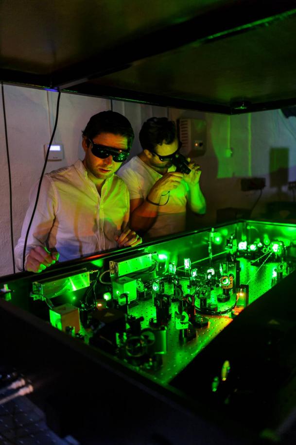
A research group at Lund University in Sweden has developed a video camera* that can record at a rate equivalent to five trillion images per second, or events as short as 0.2 trillionths of a second. This is far faster than has previously been possible (100,000 images per second).

The new super-fast camera can capture rapid processes in chemistry, physics, biology and biomedicine that so far have not been caught on film.

To illustrate the technology, the researchers have successfully filmed how light travels a distance corresponding to the thickness of paper. In reality, it only takes a picosecond, but the process has been slowed down by a trillion times.

Currently, high-speed cameras capture images one by one in a sequence. The new technology is based on an innovative algorithm, and instead captures several coded images in one picture. It then sorts them into a video sequence afterwards.

Coded flashes

The method involves exposing what you are recording (for example a chemical reaction) to light in the form of laser flashes, where each light pulse is given a unique code. The object reflects the light flashes, which merge into the single photograph. They are subsequently separated by detecting the keys.

The camera is initially intended to be used by researchers who literally want to gain better insight into many of the extremely rapid processes that occur in nature. Many take place on a picosecond and femtosecond scale.

“This does not apply to all processes in nature, but quite a few, for example, explosions, plasma flashes, turbulent combustion, brain activity in animals and chemical reactions. We are now able to ‘film’ such extremely short processes”, says professor Elias Kristensson. “In the long term, the technology can also be used by industry and others.”

“Today, the only way to visualize such rapid events is to photograph still images of the process. You then have to attempt to repeat identical experiments to provide several still images which can later be edited into a movie. The problem with this approach is that it is highly unlikely that a process will be identical if you repeat the experiment”, he says.

The researchers are currently conducting research on combustion — an area known to be difficult and complicated to study. The ultimate purpose of this basic research is to make next-generation car engines, gas turbines, and boilers cleaner and more fuel-efficient. Combustion is controlled by a number of ultra-fast processes at the molecular level, which can now be captured.

For example, the researchers will study the chemistry of plasma discharges, the lifetime of quantum states in combustion environments and in biological tissue, as well as how chemical reactions are initiated.

The research has been published in the journal Light: Science and Applications. A German company has already developed a prototype of the technology, which should be available commercially in two years.

* The technology, named FRAME (Frequency Recognition Algorithm for Multiple Exposures), uses a  camera with a flash, using “coded” light flashes, as a form of encryption. Every time a coded light flash hits the object — for example, a chemical reaction in a burning flame — the object emits an image signal (response) with the exact same coding. The following light flashes all have different codes, and the image signals are captured in one single photograph. These coded image signals are subsequently separated using an encryption key on a computer.

An atomically thin layer of water stores more energy and delivers it faster, researchers discover

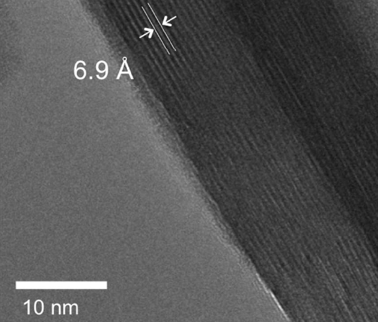
A high-resolution transmission electron microscope image of layered, crystalline tungsten oxide dihydrate, which acts as a better supercapacitor (similar to a battery) than plain tungsten oxide (without the water layer). The “stripes” are individual layers of atoms separated by atomically thin water layers; the gray area on the left is empty space. 6.9 Angstrom = 0.69 nanometer. (credit: James B. Mitchell et al./Chemistry of Materials)

Researchers at North Carolina State University have found that a material* that incorporates atomically thin layers of water can store more energy and deliver it much more quickly than the same material without the water.

The proof-of-concept finding could “ultimately lead to things like thinner batteries, faster storage for renewable-based power grids, or faster acceleration in electric vehicles,” according to Veronica Augustyn, an assistant professor of materials science and engineering at NC State and corresponding author of a paper in the journal Chemistry of Materials describing the work.

A basic goal of current energy-storage research is to combine the high energy-density (amount of energy stored) of batteries with the high power density (speed of charge/discharge) of capacitors. The new finding is a step in that direction — it could allow for an increased amount of energy to be stored per unit of volume, faster diffusion of ions through the material, and faster charge and discharge.

Crystallographic structures of tungsten oxide dihydrate (WO3.2H2O) and tungsten oxide (WO3). Dehydration of the layered hydrated phase (left) under heat treatment in air or in vacuum yields the anhydrous structure (right). (credit: James B. Mitchell et al./Chemistry of Materials)

In this research, the scientists compared two materials: a crystalline tungsten oxide and a layered, crystalline tungsten oxide dihydrate, which consists of crystalline tungsten oxide layers separated by atomically thin layers of water. When charging the two materials for 10 minutes, the researchers found that the regular tungsten oxide version stored more energy than the hydrate version. But when the charging period was only 12 seconds, the hydrate version surprisingly stored more energy than the regular material and stored energy more efficiently, wasting less energy as heat.

“Incorporating these solvent layers could be a new strategy for high-powered energy-storage devices that make use of layered materials,” Augustyn says. “We think the water layer acts as a pathway that facilitates the transfer of ions through the material. We are now moving forward with National Science Foundation-funded work on how to fine-tune this ‘interlayer,’ which will hopefully advance our understanding of these materials and get us closer to next-generation energy-storage devices.”

* The new material acts as a “pseudosupercapacitor” (between a battery and a supercapacitor, which is used in applications requiring many rapid charge/discharge cycles rather than long term compact energy storage, such as in cars, buses, and trains). The new material improves both energy density and power density. 


Abstract of Transition from Battery to Pseudocapacitor Behavior via Structural Water in Tungsten Oxide

The kinetics of energy storage in transition metal oxides are usually limited by solid-state diffusion, and the strategy most often utilized to improve their rate capability is to reduce ion diffusion distances by utilizing nanostructured materials. Here, another strategy for improving the kinetics of layered transition metal oxides by the presence of structural water is proposed. To investigate this strategy, the electrochemical energy storage behavior of a model hydrated layered oxide, WO3·2H2O, is compared with that of anhydrous WO3 in an acidic electrolyte. It is found that the presence of structural water leads to a transition from battery-like behavior in the anhydrous WO3 to ideally pseudocapacitive behavior in WO3·2H2O. As a result, WO3·2H2O exhibits significantly improved capacity retention and energy efficiency for proton storage over WO3 at sweep rates as fast as 200 mV s–1, corresponding to charge/discharge times of just a few seconds. Importantly, the energy storage of WO3·2H2O at such rates is nearly 100% efficient, unlike in the case of anhydrous WO3. Pseudocapacitance in WO3·2H2O allows for high-mass loading electrodes (>3 mg cm–2) and high areal capacitances (>0.25 F cm–2 at 200 mV s–1) with simple slurry-cast electrodes. These results demonstrate a new approach for developing pseudocapacitance in layered transition metal oxides for high-power energy storage, as well as the importance of energy efficiency as a metric of performance of pseudocapacitive materials.

Quadriplegia patient uses brain-computer interface to move his arm by just thinking

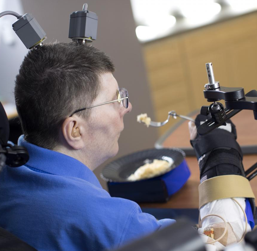
Bill Kochevar, who was paralyzed below his shoulders in a bicycling accident eight years ago, is the first person with quadriplegia to have arm and hand movements restored without robot help (credit: Case Western Reserve University/Cleveland FES Center)

A research team led by Case Western Reserve University has developed the first implanted brain-recording and muscle-stimulating system to restore arm and hand movements for quadriplegic patients.*

In a proof-of-concept experiment, the system included a brain-computer interface with recording electrodes implanted under his skull and a functional electrical stimulation (FES) system that activated his arm and hand — reconnecting his brain to paralyzed muscles.

The research was part of the ongoing BrainGate2 pilot clinical trial being conducted by a consortium of academic and other institutions to assess the safety and feasibility of the implanted brain-computer interface (BCI) system in people with paralysis. Previous Braingate designs required a robot arm.

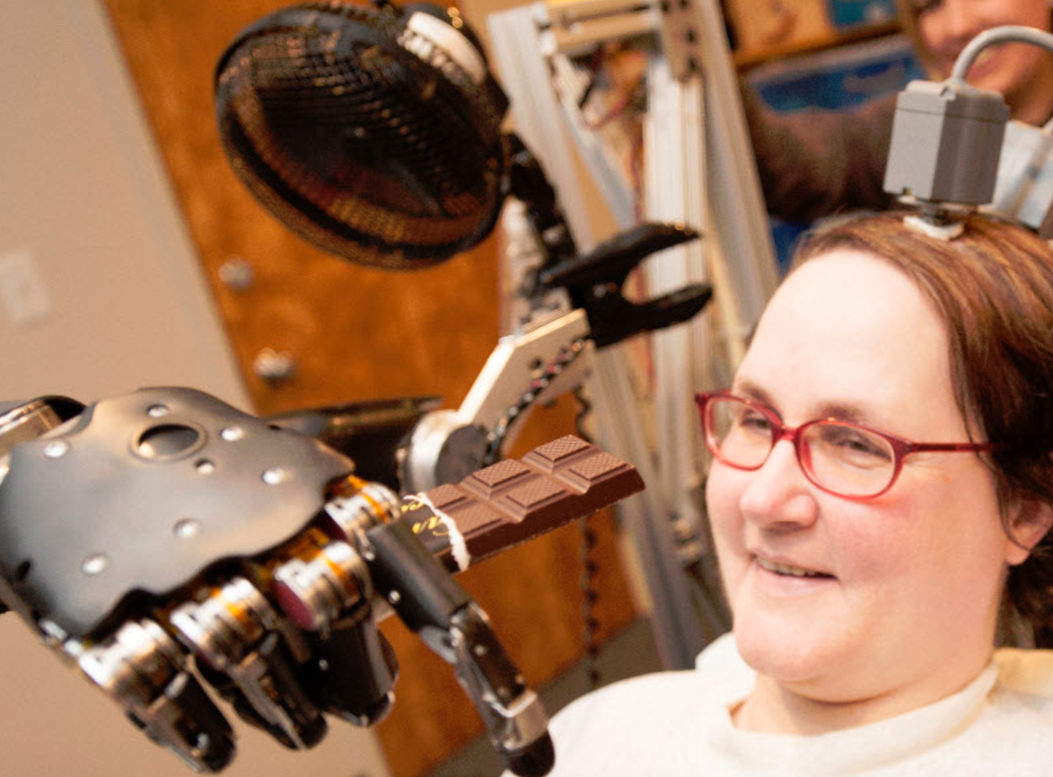
In 2012 research, Jan Scheuermann, who has quadriplegia, was able to feed herself using a brain-machine interface and a computer-driven robot arm (credit: UPMC)

Kochevar’s eight years of muscle atrophy first required rehabilitation. The researchers exercised Kochevar’s arm and hand with cyclical electrical stimulation patterns. Over 45 weeks, his strength, range of motion. and endurance improved. As he practiced movements, the researchers adjusted stimulation patterns to further his abilities.

To prepare him to use his arm again, Kochevar learned how to use his own brain signals to move a virtual-reality arm on a computer screen. The team then implanted the FES systems’ 36 electrodes that animate muscles in the upper and lower arm, allowing him to move the actual arm.

Kochevar can now make each joint in his right arm move individually. Or, just by thinking about a task such as feeding himself or getting a drink, the muscles are activated in a coordinated fashion.

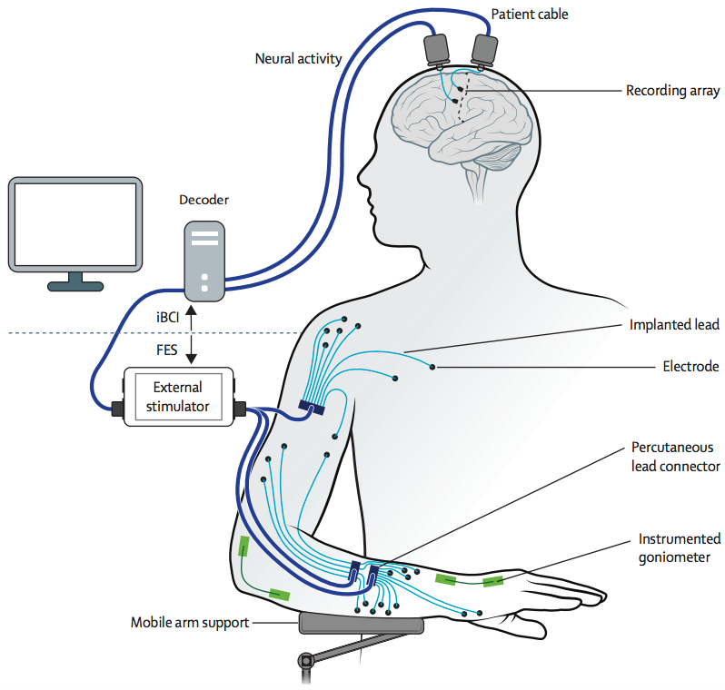
Neural activity (generated when Kochevar imagines movement of his arm and hand) is recorded from two 96-channel microelectrode arrays implanted in the motor cortex, on the surface of the brain. The implanted brain-computer interface translates the recorded brain signals into specific command signals that determine the amount of stimulation to be applied to each functional electrical stimulation (FES) electrode in the hand, wrist, arm, elbow and shoulder, and to a mobile arm support. (credit: A Bolu Ajiboye et al./The Lancet)

“Our research is at an early stage, but we believe that this neuro-prosthesis could offer individuals with paralysis the possibility of regaining arm and hand functions to perform day-to-day activities, offering them greater independence,” said lead author Dr Bolu Ajiboye, Case Western Reserve University. “So far, it has helped a man with tetraplegia to reach and grasp, meaning he could feed himself and drink. With further development, we believe the technology could give more accurate control, allowing a wider range of actions, which could begin to transform the lives of people living with paralysis.”

Work is underway to make the brain implant wireless, and the investigators are improving decoding and stimulation patterns needed to make movements more precise. Fully implantable FES systems have already been developed and are also being tested in separate clinical research.

A study of the work was published in the The Lancet March 28, 2017.

Writing in a linked Comment to The Lancet, Steve Perlmutter, M.D., University of Washington, said: “The goal is futuristic: a paralysed individual thinks about moving her arm as if her brain and muscles were not disconnected, and implanted technology seamlessly executes the desired movement… This study is groundbreaking as the first report of a person executing functional, multi-joint movements of a paralysed limb with a motor neuro-prosthesis. However, this treatment is not nearly ready for use outside the lab. The movements were rough and slow and required continuous visual feedback, as is the case for most available brain-machine interfaces, and had restricted range due to the use of a motorised device to assist shoulder movements… Thus, the study is a proof-of-principle demonstration of what is possible, rather than a fundamental advance in neuro-prosthetic concepts or technology. But it is an exciting demonstration nonetheless, and the future of motor neuro-prosthetics to overcome paralysis is brighter.”

* The study was funded by the US National Institutes of Health and the US Department of Veterans Affairs. It was conducted by scientists from Case Western Reserve University, Department of Veterans Affairs Medical Center, University Hospitals Cleveland Medical Center, MetroHealth Medical Center, Brown University, Massachusetts General Hospital, Harvard Medical School, Wyss Center for Bio and Neuroengineering. The investigational BrainGate technology was initially developed in the Brown University laboratory of John Donoghue, now the founding director of the Wyss Center for Bio and Neuroengineering in Geneva, Switzerland. The implanted recording electrodes are known as the Utah array, originally designed by Richard Normann, Emeritus Distinguished Professor of Bioengineering at the University of Utah. The report in Lancet is the result of a long-running collaboration between Kirsch, Ajiboye and the multi-institutional BrainGate consortium. Leigh Hochberg, a neurologist and neuroengineer at Massachusetts General Hospital, Brown University and the VA RR&D Center for Neurorestoration and Neurotechnology in Providence, Rhode Island, directs the pilot clinical trial of the BrainGate system and is a study co-author.


Case | Man with quadriplegia employs injury bridging technologies to move again – just by thinking


Abstract of Restoration of reaching and grasping movements through brain-controlled muscle stimulation in a person with tetraplegia: a proof-of-concept demonstration

Background: People with chronic tetraplegia, due to high-cervical spinal cord injury, can regain limb movements through coordinated electrical stimulation of peripheral muscles and nerves, known as functional electrical stimulation (FES). Users typically command FES systems through other preserved, but unrelated and limited in number, volitional movements (eg, facial muscle activity, head movements, shoulder shrugs). We report the findings of an individual with traumatic high-cervical spinal cord injury who coordinated reaching and grasping movements using his own paralysed arm and hand, reanimated through implanted FES, and commanded using his own cortical signals through an intracortical brain–computer interface (iBCI).

Methods: We recruited a participant into the BrainGate2 clinical trial, an ongoing study that obtains safety information regarding an intracortical neural interface device, and investigates the feasibility of people with tetraplegia controlling assistive devices using their cortical signals. Surgical procedures were performed at University Hospitals Cleveland Medical Center (Cleveland, OH, USA). Study procedures and data analyses were performed at Case Western Reserve University (Cleveland, OH, USA) and the US Department of Veterans Affairs, Louis Stokes Cleveland Veterans Affairs Medical Center (Cleveland, OH, USA). The study participant was a 53-year-old man with a spinal cord injury (cervical level 4, American Spinal Injury Association Impairment Scale category A). He received two intracortical microelectrode arrays in the hand area of his motor cortex, and 4 months and 9 months later received a total of 36 implanted percutaneous electrodes in his right upper and lower arm to electrically stimulate his hand, elbow, and shoulder muscles. The participant used a motorised mobile arm support for gravitational assistance and to provide humeral abduction and adduction under cortical control. We assessed the participant’s ability to cortically command his paralysed arm to perform simple single-joint arm and hand movements and functionally meaningful multi-joint movements. We compared iBCI control of his paralysed arm with that of a virtual three-dimensional arm. This study is registered with ClinicalTrials.gov, number NCT00912041.

Findings: The intracortical implant occurred on Dec 1, 2014, and we are continuing to study the participant. The last session included in this report was Nov 7, 2016. The point-to-point target acquisition sessions began on Oct 8, 2015 (311 days after implant). The participant successfully cortically commanded single-joint and coordinated multi-joint arm movements for point-to-point target acquisitions (80–100% accuracy), using first a virtual arm and second his own arm animated by FES. Using his paralysed arm, the participant volitionally performed self-paced reaches to drink a mug of coffee (successfully completing 11 of 12 attempts within a single session 463 days after implant) and feed himself (717 days after implant).

Interpretation: To our knowledge, this is the first report of a combined implanted FES+iBCI neuroprosthesis for restoring both reaching and grasping movements to people with chronic tetraplegia due to spinal cord injury, and represents a major advance, with a clear translational path, for clinically viable neuroprostheses for restoration of reaching and grasping after paralysis.

Funding: National Institutes of Health, Department of Veterans Affairs.

The first 2D microprocessor — based on a layer of just 3 atoms

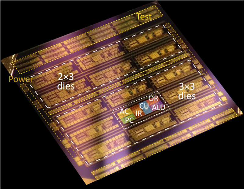
Overview of the entire chip. AC = Accumulator, internal buffer; PC = Program Counter, points at the next instruction to be executed; IR = Instruction Register, used to buffer data- and instruction-bits received from the external memory; CU = Control Unit, orchestrates the other units according to the instruction to be executed; OR = Output Register, memory used to buffer output-data; ALU = Arithmetic Logic Unit, does the actual calculations. (credit: TU Wien)

Researchers at Vienna University of Technology (known as TU Wien) in Vienna, Austria, have developed the world’s first two-dimensional microprocessor — the most complex 2D circuitry so far. Microprocessors based on atomically thin 2D materials promise to one day replace traditional microprocessors as well as open up new applications in flexible electronics.

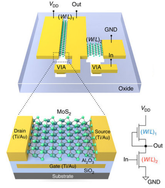
Consisting of 115 transistors, the microprocessor can run, simple user-defined programs stored in an external memory, perform logical operations, and communicate with peripheral devices. The microprocessor is based on molybdenum disulphide (MoS2), a three-atoms-thick 2D semiconductor transistor layer consisting of molybdenum and sulphur atoms, with a surface area of around 0.6 square millimeters.

Schematic drawing of an inverter (“NOT” logic) circuit (top) and an individual MoS2 transistor (bottom) (credit: Stefan Wachter et al./Nature Communications)

For demonstration purposes, the microprocessor is currently a 1-bit design, but it’s scalable to a multi-bit design using industrial fabrication methods, says Thomas Mueller, PhD., team leader and senior author of an open-access paper on the research published in Nature Communications.*

New sensors and flexible displays

Two-dimensional materials are flexible, making future 2D microprocessors and other integrated circuits ideal for uses such as medical sensors and flexible displays. They promise to extend computing to the atomic level, as silicon reaches its physical limits.

However, to date, it has only been possible to produce individual 2D digital components using a few transistors. The first 2D MoS2 transistor with a working 1-nanometer (nm) gate was created in October 2016 by a team led by Lawrence Berkeley National Laboratory (Berkeley Lab) scientists, as KurzweilAI reported.

Mueller said much more powerful and complex circuits with thousands or even millions of transistors will be required for this technology to have practical applications. Reproducibility continues to be one of the biggest challenges currently being faced within this field of research, along with the yield in the production of the transistors used, he explained.

* “We also gave careful consideration to the dimensions of the individual transistors,” explains Mueller. “The exact relationships between the transistor geometries within a basic circuit component are a critical factor in being able to create and cascade more complex units. … the major challenge that we faced during device fabrication is yield. Although the yield for subunits was high (for example, ∼80% of ALUs were fully functional), the sheer complexity of the full system, together with the non-fault tolerant design, resulted in an overall yield of only a few per cent of fully functional devices. Imperfections of the MoS2 film, mainly caused by the transfer from the growth to the target substrate, were identified as main source for device failure. However, as no metal catalyst is required for the synthesis of TMD films, direct growth on the target substrate is a promising route to improve yield.


Abstract of A microprocessor based on a two-dimensional semiconductor

The advent of microcomputers in the 1970s has dramatically changed our society. Since then, microprocessors have been made almost exclusively from silicon, but the ever-increasing demand for higher integration density and speed, lower power consumption and better integrability with everyday goods has prompted the search for alternatives. Germanium and III–V compound semiconductors are being considered promising candidates for future high-performance processor generations and chips based on thin-film plastic technology or carbon nanotubes could allow for embedding electronic intelligence into arbitrary objects for the Internet-of-Things. Here, we present a 1-bit implementation of a microprocessor using a two-dimensional semiconductor—molybdenum disulfide. The device can execute user-defined programs stored in an external memory, perform logical operations and communicate with its periphery. Our 1-bit design is readily scalable to multi-bit data. The device consists of 115 transistors and constitutes the most complex circuitry so far made from a two-dimensional material.

What if you could type directly from your brain at 100 words per minute?

(credit: Facebook)

Regina Dugan, PhD, Facebook VP of Engineering, Building8, revealed today (April 19, 2017) at Facebook F8 conference 2017 a plan to develop a non-invasive brain-computer interface that will let you type at 100 wpm — by decoding neural activity devoted to speech.

Dugan previously headed Google’s Advanced Technology and Projects Group, and before that, was Director of the Defense Advanced Research Projects Agency (DARPA).

She explained in a Facebook post that over the next two years, her team will be building systems that demonstrate “a non-invasive system that could one day become a speech prosthetic for people with communication disorders or a new means for input to AR [augmented reality].”

Dugan said that “even something as simple as a ‘yes/no’ brain click … would be transformative.” That simple level has been achieved by using functional near-infrared spectroscopy (fNIRS) to measure changes in blood oxygen levels in the frontal lobes of the brain, as KurzweilAI recently reported. (Near-infrared light can penetrate the skull and partially into the brain.)

Dugan agrees that optical imaging is the best place to start, but her Building8 team team plans to go way beyond that research — sampling hundreds of times per second and precise to millimeters. The research team began working on the brain-typing project six months ago and she now has a team of more than 60 researchers who specialize in optical neural imaging systems that push the limits of spatial resolution and machine-learning methods for decoding speech and language.

The research is headed by Mark Chevillet, previously an adjunct professor of neuroscience at Johns Hopkins University.

Besides replacing smartphones, the system would be a powerful speech prosthetic, she noted — allowing paralyzed patients to “speak” at normal speed.

(credit: Facebook)

Dugan revealed one specific method the researchers are currently working on to achieve that: a ballistic filter for creating quasi ballistic photons (avoiding diffusion) — creating a narrow beam for precise targeting — combined with a new method of detecting blood-oxygen levels.

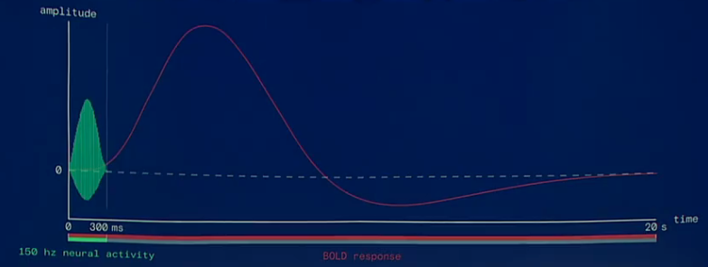
Neural activity (in green) and associated blood oxygenation level dependent (BOLD) waveform (credit: Facebook)

Dugan also described a system that may one day allow hearing-impaired people to hear directly via vibrotactile sensors embedded in the skin. “In the 19th century, Braille taught us that we could interpret small bumps on a surface as language,” she said. “Since then, many techniques have emerged that illustrate our brain’s ability to reconstruct language from components.” Today, she demonstrated “an artificial cochlea of sorts and the beginnings of a new a ‘haptic vocabulary’.”

A Facebook engineer with acoustic sensors implanted in her arm has learned to feel the acoustic shapes corresponding to words (credit: Facebook)

Dugan’s presentation can be viewed in the F8 2017 Keynote Day 2 video (starting at 1:08:10).


(credit: Facebook)

Nanopores map small changes in DNA for early cancer detection

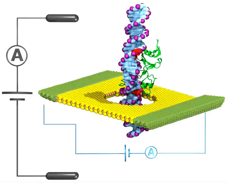
To detect DNA methylation changes (for cancer early warning), researchers punched a tiny hole (pore) in a flat sheet of graphene (or other  2D material). They then submerged the material in a salt solution and applied an electrical voltage to force the DNA molecule through the pore. A dip in the ionic current (black A) identified a methyl group (green) is passing through, but a dip in the electrical current (blue A) could detect smaller DNA changes. (credit: Beckman Institute Nanoelectronics and Nanomaterials Group)

University of Illinois researchers have designed a high-resolution method to detect, count, and map tiny additions to DNA called methylations*, which can be a early-warning sign of cancer.

The method threads DNA strands through a tiny hole, called a nanopore, in an atomically thin sheet of graphene or other 2D material** with an electrical current running through it.

Many methylations packed close together suggest an early stage of cancer, explained study leader Jean-Pierre Leburton, a professor of electrical and computer engineering at Illinois.

There have been previous attempts to use nanopores to detect methylation (by measuring ionic changes), which have been limited in resolution (how precise the measurement is). The Illinois group instead applied a current directly to the conductive sheet surrounding the pore. Working with Klaus Schulten, a professor of physics at Illinois, Leburton’s group at Illinois’ Beckman Institute for Advanced Science and Technology, they used advanced computer simulations to test applying current to different flat materials, such as graphene and molybdenum disulfide, while methylated DNA was threaded through.

“Our simulations indicate that measuring the current through the membrane instead of just the solution around it is much more precise,” Leburton said. “If you have two methylations close together, even only 10 base pairs away, you continue to see two dips and no overlapping. We also can map where they are on the strand, so we can see how many there are and where they are.”

Leburton’s group is now working with collaborators to improve DNA threading, to cut down on noise in the electrical signal, and to perform experiments to verify their simulations.

The study was published in 2D Materials and Applications, a new open-access journal from Nature Press. Grants from Oxford Nanopore Technology, the Beckman Institute, the National Institutes of Health, and the National Science Foundation supported this work.

* Methylation refers to the addition of a methyl group, which contains one carbon atom bonded to three hydrogen atoms, with the formula CH3.

** Such as graphene and molybdenum disulfide (MoS2).


NewsIllinois | Nanopore detection of DNA methylation