Neuron-recording nanowires could help screen drugs for neurological diseases

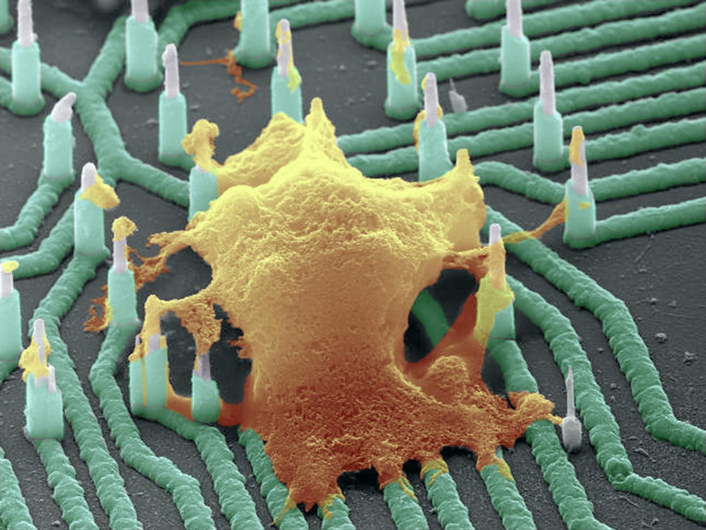
Colorized scanning electron microscopy (SEM) image of a neuron (orange) interfaced with the nanowire array (green). (credit: Integrated Electronics and Biointerfaces Laboratory, UC San Diego)

A research team* led by engineers at the University of California San Diego has developed nanowire technology that can non-destructively record the electrical activity of neurons in fine detail.

The new technology, published April 10, 2017 in Nano Letters, could one day serve as a platform to screen drugs for neurological diseases and help researchers better understand how single cells communicate in large neuronal networks.

A brain implant

The researchers currently create the neurons in vitro (in the lab) from human induced pluripotent stem cells. But the ultimate goal is to “translate this technology to a device that can be implanted in the brain,” said Shadi Dayeh, PhD, an electrical engineering professor at the UC San Diego Jacobs School of Engineering and the team’s lead investigator.

The technology can uncover details about a neuron’s health, activity, and response to drugs by measuring ion channel currents and changes in the neuron’s intracellular voltage (generated by the difference in ion concentration between the inside and outside of the cell).

The researchers cite five key innovations of this new nanowire-to-neuron technology:

  • It’s nondestructive (unlike current methods, which can break the cell membrane and eventually kill the cell).
  • It can simultaneously measure voltage changes in multiple neurons and in the future could bridge or repair neurons.**
  • It can isolate the electrical signal measured by each individual nanowire, with high sensitivity and high signal-to-noise ratios. Existing techniques are not scalable to 2D and 3D tissue-like structures cultured in vitro, according to Dayeh.
  • It can also be used for heart-on-chip drug screening for cardiac diseases.
  • The nanowires can integrate with CMOS (computer chip) electronics.***
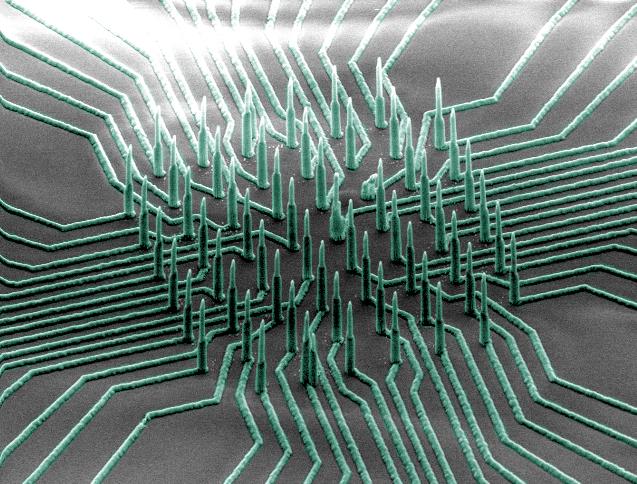
A colorized scanning electron microscopy (SEM) image of the silicon-nickel-titanium nanowire array. The nanowires are densely packed on a small chip that is compatible with CMOS chips. The nanowires poke inside cells without damaging them, and are sensitive enough to measure small voltage changes (millivolt or less). (credit: Integrated Electronics and Biointerfaces Laboratory, UC San Diego)

* The project was a collaborative effort between researchers at UC San Diego, the Conrad Prebys Center for Chemical Genomics at the Sanford Burnham Medical Research Institute, Nanyang Technological University in Singapore, and Sandia National Laboratories. This work was supported by the National Science Foundation, the Center for Brain Activity Mapping at UC San Diego, Qualcomm Institute at UC San Diego, Los Alamos National Laboratory, the National Institutes of Health, the March of Dimes, and UC San Diego Frontiers of Innovation Scholar Program. Dayeh’s laboratory holds several pending patent applications for this technology.

** “Highly parallel in vitro drug screening experiments can be performed using the human-relevant iPSC cell line and without the need of the laborious patch-clamp … which is destructive and unscalable to large neuronal densities and to long recording times, or planar multielectrode arrays that enable long-term recordings but can just measure extracellular potentials and lack the sensitivity to subthreshold potentials. … In vivo targeted modulation of individual neural circuits or even single cells within a network becomes possible, and implications for bridging or repairing networks in neurologically affected regions become within reach.” — Ren Liu et al./Nanoletters

*** The researchers invented a new wafer bonding approach to fuse the silicon nanowires to the nickel electrodes. Their approach involved a process called silicidation, which is a reaction that binds two solids (silicon and another metal) together without melting either material. This process prevents the nickel electrodes from liquidizing, spreading out and shorting adjacent electrode leads. Silicidation is usually used to make contacts to transistors, but this is the first time it is being used to do patterned wafer bonding, Dayeh said. “And since this process is used in semiconductor device fabrication, we can integrate versions of these nanowires with CMOS electronics, but it still needs further optimization for brain-on-chip drug screening.”


Abstract of High Density Individually Addressable Nanowire Arrays Record Intracellular Activity from Primary Rodent and Human Stem Cell Derived Neurons

We report a new hybrid integration scheme that offers for the first time a nanowire-on-lead approach, which enables independent electrical addressability, is scalable, and has superior spatial resolution in vertical nanowire arrays. The fabrication of these nanowire arrays is demonstrated to be scalable down to submicrometer site-to-site spacing and can be combined with standard integrated circuit fabrication technologies. We utilize these arrays to perform electrophysiological recordings from mouse and rat primary neurons and human induced pluripotent stem cell (hiPSC)-derived neurons, which revealed high signal-to-noise ratios and sensitivity to subthreshold postsynaptic potentials (PSPs). We measured electrical activity from rodent neurons from 8 days in vitro (DIV) to 14 DIV and from hiPSC-derived neurons at 6 weeks in vitro post culture with signal amplitudes up to 99 mV. Overall, our platform paves the way for longitudinal electrophysiological experiments on synaptic activity in human iPSC based disease models of neuronal networks, critical for understanding the mechanisms of neurological diseases and for developing drugs to treat them.

Glowing nanoparticles open new window for live optical biological imaging

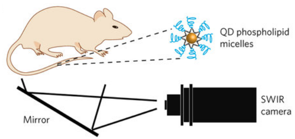
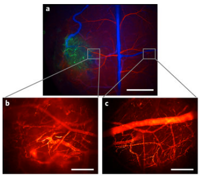
(a) High-resolution, high-speed quantum-dot shortwave infrared imaging was used to image the blood-vessel network of a mouse glioblastoma brain tumor (b) at 60 frames per second and to compare it to the blood-vessel network (c) in the opposite (healthy) brain hemisphere. (credit: Oliver T. Bruns et al./ Nature Biomedical Engineering)

A team of researchers has created bright, glowing nanoparticles called quantum dots that can be injected into the body, where they emit light at shortwave infrared (SWIR) wavelengths that pass through the skin — allowing internal body structures such as fine networks of blood vessels to be imaged in vivo (in live animals) on high-speed video cameras for the first time.

The new findings are described in an open-access paper in the journal Nature Biomedical Engineering by Moungi Bawendi, MIT Lester Wolf Professor of Chemistry, and 22 other researchers.*

Near-infrared imaging for research on biological tissues, with wavelengths between 700 and 900 nanometers (billionths of a meter), is widely used because these wavelengths can shine through tissues. But wavelengths of around 1,000 to 2,000 nanometers have the potential to provide even better results, because body tissues are more transparent at that longer light-wavelength range.

The problem in doing that has been the lack of light-emitting materials that could work at those longer wavelengths and that were bright enough to be easily detected through the surrounding skin and muscle tissues.

Live internal images of awake, moving mice

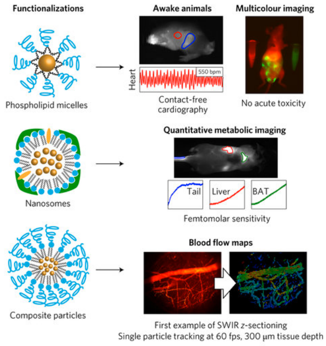
Contact-free video monitoring of heart and respiratory rate in mice using quantum dots covered with biocompatible lipid molecules and injected into mice. A newly developed camera is highly sensitive to shortwave infrared light. (credit: Oliver T. Bruns et al./ Nature Biomedical Engineering)

Now the team has succeeded in making particles that are “orders of magnitude better than previous materials, and that allow unprecedented detail in biological imaging,” says lead author Oliver T. Bruns, an MIT research scientist. The synthesis of these new particles was initially described in an open-access paper by researchers from the Bawendi group in Nature Communications last year.

These new light-emitting nanoparticles are the first that are bright enough to allow imaging of internal organs in mice that are awake and moving, as opposed to previous methods that required them to be anesthetized, Bruns says. Initial applications would be for preclinical research in animals, as the compounds contain some materials, such as indium arsenide, that are unlikely to be approved for use in humans. The researchers are also working on developing versions that would be safer for humans.

Quantum dots, made of semiconductor materials, emit light whose frequency can be precisely tuned by controlling the exact size and composition of the particles. These were functionalized via three distinct surface coatings that tailor the physiological properties for specific shortwave infrared imaging applications. The quantum dots are so bright, their emissions can be captured with very short exposure times. That makes it possible to produce not just single images but video that captures details of motion, such as the flow of blood — making it possible to distinguish between veins and arteries. (credit: Oliver T. Bruns et al./ Nature Biomedical Engineering)

Not only can the new method determine the direction of blood flow, Bruns says, it is detailed enough to track individual blood cells within that flow. “We can track the flow in each and every capillary, at super-high speed,” he says. “We can get a quantitative measure of flow, and we can do such flow measurements at very high resolution, over large areas.”

Such imaging could potentially be used, for example, to study how the blood flow pattern in a tumor changes as the tumor develops, which might lead to new ways of monitoring disease progression or responsiveness to a drug treatment. “This could give a good indication of how treatments are working that was not possible before,” he says.

* The team included members from Harvard Medical School, the Harvard T.H. Chan School of Public Health, Raytheon Vision Systems, and University Medical Center in Hamburg, Germany. The work was supported by the National Institutes of Health, the National Cancer Institute, the National Foundation for Cancer Research, the Warshaw Institute for Pancreatic Cancer Research, the Massachusetts General Hospital Executive Committee on Research, the Army Research Office through the Institute for Soldier Nanotechnologies at MIT, the U.S. Department of Defense, and the National Science Foundation.

This contact lens could someday measure blood glucose and other signs of disease

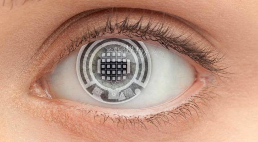
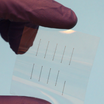
Transparent biosensors in contact lenses (made visible in this artist’s rendition) could soon help track our health. (credit: Jack Forkey/Oregon State University)

Transparent biosensors embedded into contact lenses could soon allow doctors and patients to monitor blood glucose levels and many other telltale signs of disease from teardops without invasive tests, according to Oregon State University chemical engineering professor Gregory S. Herman, Ph.D. who presented his work Tuesday April 4, 2017 at the American Chemical Society (ACS) National Meeting & Exposition.

Herman and two colleagues previously invented a compound composed of indium gallium zinc oxide (IGZO). This semiconductor is the same one that has revolutionized electronics, providing higher resolution displays on televisions, smartphones and tablets while saving power and improving touch-screen sensitivity.

In his research, Herman’s goal was to find a way to help people with diabetes continuously monitor their blood glucose levels more efficiently using bio-sensing contact lenses. Continuous glucose monitoring — instead of the prick-and-test approach — helps reduce the risk of diabetes-related health problems. But most continuous glucose monitoring systems require inserting electrodes in various locations under the skin. This can be painful, and the electrodes can cause skin irritation or infections.

Herman says bio-sensing contact lenses could eliminate many of these problems and improve compliance since users can easily replace them on a daily basis. And, unlike electrodes on the skin, they are invisible, which could help users feel less self-conscious about using them.

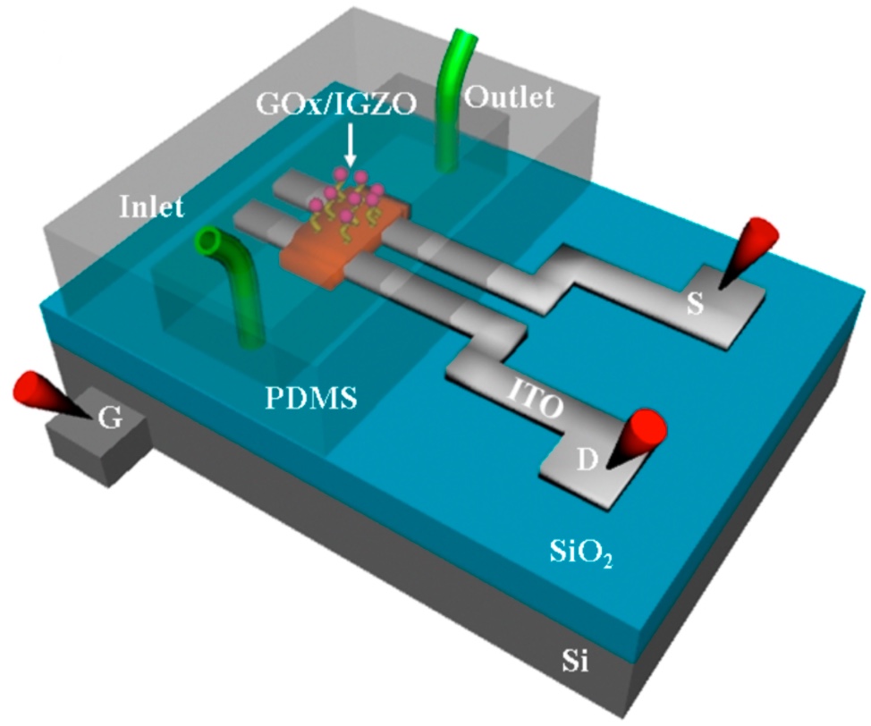
A schematic illustration of an experimental device (credit: Du X et al./ ACS Applied Materials & Interfaces)

To test this idea, Herman and his colleagues first developed an inexpensive method to make IGZO electronics. Then, they used the approach to fabricate a biosensor containing a transparent sheet of IGZO field-effect transistors and glucose oxidase, an enzyme that breaks down glucose. When they added glucose to the mixture, the enzyme oxidized the blood sugar. As a result, the pH level in the mixture shifted and, in turn, triggered changes in the electrical current flowing through the IGZO transistor.

In conventional biosensors, these electrical changes would be used to measure the glucose concentrations in the interstitial fluid under a patient’s skin. But glucose concentrations are much lower in the eye. So any biosensors embedded into contact lenses will need to be far more sensitive. To address this problem, the researchers created nanostructures within the IGZO biosensor that were able to detect glucose concentrations much lower than found in tears.*

In theory, Herman says, more than 2,000 transparent biosensors — each measuring a different bodily function — could be embedded in a 1-millimeter square patch of an IGZO contact lens. Once developed, the biosensors could transmit vital health information to smartphones and other Wi-Fi or Bluetooth-enabled devices.

Herman’s team has already used the IGZO system in catheters to measure uric acid, a key indicator of kidney function, and is exploring the possibility of using it for early detection of cancer and other serious conditions. However, Herman says it could be a year or more before a prototype bio-sensing contact lens is ready for animal testing.

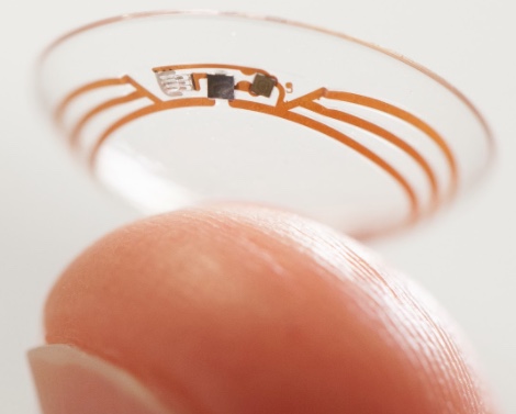
(credit: Google)

The concept appears similar to Goggle’s smart contact lens project, using a tiny wireless chip and miniaturized glucose sensor that are embedded between two layers of soft contact lens material, announced in 2014, but Herman says the Google design is more limited and that the research has stalled.

Herman acknowledges funding from the Juvenile Diabetes Research Foundation and the Northwest Nanotechnology Infrastructure, a member of the National Nanotechnology Coordinated Infrastructure, which is supported by the National Science Foundation.

* “We have functionalized the back-channel of IGZO-FETs with aminosilane groups that are cross-linked to glucose oxidase and have demonstrated that these devices have high sensitivity to changes in glucose concentrations. Glucose sensing occurs through the decrease in pH during glucose oxidation, which modulates the positive charge of the aminosilane groups attached to the IGZO surface. The change in charge affects the number of acceptor-like surface states which can deplete electron density in the n-type IGZO semiconductor. Increasing glucose concentrations leads to an increase in acceptor states and a decrease in drain-source conductance due to a positive shift in the turn-on voltage. The functionalized IGZO-FET devices are effective in minimizing detection of interfering compounds including acetaminophen and ascorbic acid.” — Du XLi YMotley JRStickle WFHerman GS, Glucose Sensing Using Functionalized Amorphous In-Ga-Zn-O Field-Effect Transistors. ACS Applied Materials & Interfaces. 2016 03 30.


Abstract of Implantable indium gallium zinc oxide field effect biosensors

Amorphous indium gallium zinc oxide (IGZO) field effect transistors (FETs) are a promising technology for a wide range of electronic applications including implantable and wearable biosensors. We have recently developed novel, low-cost methods to fabricate IGZO-FETs, with a wide range of form factors. Attaching self-assembled monolayers (SAM) to the IGZO backchannel allows us to precisely control surface chemistry and improve stability of the sensors. Functionalizing the SAMs with enzymes provides excellent selectivity for the sensors, and effectively minimizes interference from acetaminophen/ascorbic acid. We have recently demonstrated that a nanostructured IGZO network can significantly improve sensitivity as a sensing transducer, compared to blanket IGZO films. In Figure (a) we show a scanning electron microscopy image of a nanostructured IGZO transducer located between two indium tin oxide source/drain electrodes. In Figure (b) we show an atomic force microscope image of the close packed hexagonal IGZO nanostructured network (3×3 mm2), and Figure (c) shows the corresponding height profile along the arrow shown in (b). We will discuss reasons for improved sensitivity for the nanostructured IGZO, and demonstrate high sensitivity for glucose sensing. Finally, fully transparent glucose sensors have been fabricated directly on catheters, and have been characterized by a range of techniques. These results suggest that IGZO-FETs may provide a means to integrate fully transparent, highly-sensitive sensors into contact lenses.

Mass production of low-cost, flexible inkjet-printed electronics

Experimental flexible resistive memory printed on a polyimide foil. The lines are silver contacts; four memory cells can be seen around the lines by zooming in. (credit: Michael Kaiser)

A group of researchers at Munich University of Applied Sciences in Germany and INRS-EMT in Canada is paving the way for mass-producing low-cost printable electronics by demonstrating a fully inkjet-printable, flexible resistive memory.*

Additive manufacturing (commonly used in 3-D printing), allows for a streamlined process flow, replacing complex lithography (used in making chips), at the detriment of feature size, which however is usually not critical for memory devices in less computationally demanding uses.

Inkjet printing allows for roll-to-roll printing, making possible mass-produced printable electronics. In an open-access paper appearing this week in Applied Physics Letters, from AIP Publishing, the group presents a proof of concept for using inkjet printing of resistive memory (ReRAM).

“We use functional inks to deposit a capacitor structure — conductor-insulator-conductor — with commercially available materials** that have already been deployed in cleanroom processes,” said Bernhard Huber, a doctoral student at INRS-EMT and working in the Laboratory for Microsystems Technology at Munich University of Applied Sciences. “This process is identical to that of an office inkjet printer, with an additional option of fine-tuning the droplet size and heating the target material.”

The process enables extremely low-cost flexible electronics and may lead to print-on-demand electronics, which shows huge potential for small, flexible lines of production and end-user products, the researchers suggest.

Examples include supermarkets printing their own smart tags, public transport providers customizing multifunctional tickets on demand, and wearables.

* Currently, computing devices use two different types of memory: a non-volatile but slow storage memory like Flash and a fast but volatile random access memory (RAM) like DRAM. Resistive RAM combines non-volatile behavior and fast read-and-write access in one device. The two memory states (0 and 1) are defined by the resistance of the memory cell.

** Silver/spin-on-glass (SOG)/poly(3,4-ethylenedioxythiophene) polystyrene sulfonate (PEDOT:PSS) cells were fabricated by inkjet printing alone. The cells feature low switching voltages, low write currents, and a high ratio between high and low resistance state of 10,000.

UPDATE April 9. 2017: “3D-printed” removed and new higher-resolution image used.


Abstract of Fully inkjet printed flexible resistive memory

Resistively switching memory cells (ReRAM) are strong contenders for next-generation non-volatile random access memories. In this paper, we present ReRAM cells on flexible substrates consisting of Ag/spin-on-glass/PEDOT:PSS (poly(3,4-ethylenedioxythiophene) polystyrene sulfonate).

The complete cell is fabricated using a standard inkjet printer without additional process steps. Investigations on the spin-on-glass insulating layer showed that low sintering temperatures are sufficient for good switching behavior, providing compatibility with various foils. The cells feature low switching voltages, low write currents, and a high ratio between high and low resistance state of 104. Combined with excellent switching characteristics under bending conditions, these results pave the way for low-power and low-cost memory devices for future applications in flexible electronics.

The next agricultural revolution: a ‘bionic leaf’ that could help feed the world

The radishes on the right were grown with the help of a bionic leaf that produces fertilizer with bacteria, sunlight, water, and air. (credit: Nocera lab, Harvard University)

Harvard University chemists have invented a new kind of “bionic” leaf that uses bacteria, sunlight, water, and air to make fertilizer right in the soil where crops are grown. It could make possible a future low-cost commercial fertilizer for poorer countries in the emerging world.

The invention deals with the renewed challenge of feeding the world as the population continues to balloon.* “When you have a large centralized process and a massive infrastructure, you can easily make and deliver fertilizer,” Daniel Nocera, Ph.D., says. “But if I said that now you’ve got to do it in a village in India onsite with dirty water — forget it. Poorer countries in the emerging world don’t always have the resources to do this. We should be thinking of a distributed system because that’s where it’s really needed.”

The research was presented at the national meeting of the American Chemical Society (ACS) today (April 3, 2017). The new bionic leaf builds on a previous Nocera-team invention: the “artificial leaf” — a device that mimics photosynthesis: When exposed to sunlight, it mimics a natural leaf by splitting water into hydrogen and oxygen. These two gases would be stored in a fuel cell, which can use those two materials to produce electricity from inexpensive materials.

That was followed by “bionic leaf 2.0,” a water-splitting system that carbon dioxide out of the air and uses solar energy plus hydrogen-eating Ralstonia eutropha bacteria to produce liquid fuel with 10 percent efficiency, compared to the 1 percent seen in the fastest-growing plants. It provided biomass and liquid fuel yields that greatly exceeded those from natural photosynthesis.

Fertilizer created from sunlight + water + carbon dioxide and nitrogen from the air

For the new “bionic leaf,” Nocera’s team has designed a system in which bacteria use hydrogen from the water split by the artificial leaf plus carbon dioxide from the atmosphere to make a bioplastic that the bacteria store inside themselves as fuel. “I can then put the bug [bacteria] in the soil because it has already used the sunlight to make the bioplastic,” Nocera says. “Then the bug pulls nitrogen from the air and uses the bioplastic, which is basically stored hydrogen, to drive the fixation cycle to make ammonia for fertilizing crops.”

The researchers have used their approach to grow five crop cycles of radishes. The vegetables receiving the bionic-leaf-derived fertilizer weigh 150 percent more than the control crops. The next step, Nocera says, is to boost throughput so that one day, farmers in India or sub-Saharan Africa can produce their own fertilizer with this method.

Nocera said a paper describing the new system will be submitted for publication in about six weeks.

* The first “green revolution” in the 1960s saw the increased use of fertilizer on new varieties of rice and wheat, which helped double agricultural production. Although the transformation resulted in some serious environmental damage, it potentially saved millions of lives, particularly in Asia, according to the United Nations (U.N.) Food and Agriculture Organization. But the world’s population continues to grow and is expected to swell by more than 2 billion people by 2050, with much of this growth occurring in some of the poorest countries, according to the U.N. Providing food for everyone will require a multi-pronged approach, but experts generally agree that one of the tactics will have to involve boosting crop yields to avoid clearing even more land for farming.


American Chemical Society | A ‘bionic leaf’ could help feed the world

This advance could finally make graphene-based semiconductor chips feasible

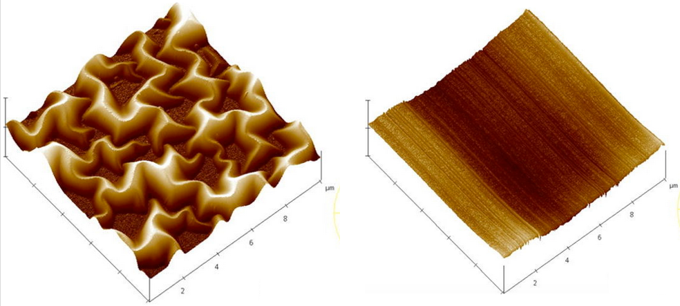
Atomic force microscopy images of as-deposited (left) and laser-annealed (right) reduced graphene oxide (rGO) thin films. The entire “pulsed laser annealing” process is done at room temperature and atmospheric pressure, using high-power laser pulses to convert p-type rGO material into n-type and completed in about one fifth of a microsecond. (credit: Anagh Bhaumik and Jagdish Narayan/Journal of Applied Physics)

Researchers at North Carolina State University (NC State) have developed a layered material that can be used to develop transistors based on graphene — a long-sought goal in the electronics industry.

Graphene has attractive properties, such as extremely high conductivity, meaning it conducts the flow of electrical current really well (compared to copper, for example), but it’s not a semiconductor, so it can’t work in a transistor (aside from providing great connections). A form of graphene called “graphene oxide” is a semiconductor, but it does not conduct well.

However, a form of graphene oxide called “reduced graphene oxide” (rGO) does conduct well*. Despite that, rGO still can’t function in a transistor. That’s because the design of a transistor is based on creating a junction between two materials: one that is positively charged (p-type) and one that is negatively charged (n-type), and native rGO is only a p-type.

The NC State researchers’ solution was to use high-powered laser pulses to disrupt chemical groups on an rGO thin film. This disruption moved electrons from one group to another, effectively converting p-type rGO to n-type rGO. They then used the two forms of rGO as two layers (a layer of n-type rGO on the surface and a layer of p-type rGO underneath) — creating a layered thin-film material that could be used to develop rGO-based transistors for use in future semiconductor chips.

The researchers were also able to integrate the rGO-based transistors onto sapphire and silicon wafers across the entire wafer.

The paper was published in the Journal of Applied Physics. The work was done with support from the National Science Foundation.

* Reduction is a chemical reaction that involves the gaining of electrons.


Abstract of Conversion of p to n-type reduced graphene oxide by laser annealing at room temperature and pressure

Physical properties of reduced graphene oxide (rGO) are strongly dependent on the ratio of sp2 to sp3hybridized carbon atoms and the presence of different functional groups in its structural framework. This research for the very first time illustrates successful wafer scale integration of graphene-related materials by a pulsed laser deposition technique, and controlled conversion of p to n-type 2D rGO by pulsed laser annealing using a nanosecond ArF excimer laser. Reduced graphene oxide is grown onto c-sapphire by employing pulsed laser deposition in a laser MBE chamber and is intrinsically p-type in nature. Subsequent laser annealing converts p into n-type rGO. The XRD, SEM, and Raman spectroscopy indicate the presence of large-area rGO onto c-sapphire having Raman-active vibrational modes: D, G, and 2D. High-resolution SEM and AFM reveal the morphology due to interfacial instability and formation of n-type rGO. Temperature-dependent resistance data of rGO thin films follow the Efros-Shklovskii variable-range-hopping model in the low-temperature region and Arrhenius conduction in the high-temperature regime. The photoluminescence spectra also reveal less intense and broader blue fluorescence spectra, indicating the presence of miniature sized sp2 domains in the vicinity of π* electronic states, which favor the VRH transport phenomena. The XPS results reveal a reduction of the rGO network after laser annealing with the C/O ratio measuring as high as 23% after laser-assisted reduction. The p to n-type conversion is due to the reduction of the rGO framework which also decreases the ratio of the intensity of the D peak to that of the G peak as it is evident from the Raman spectra. This wafer scale integration of rGO with c-sapphire and p to n-type conversion employing a laser annealing technique at room temperature and pressure will be useful for large-area electronic devices and will open a new frontier for further extensive research in graphene-based functionalized 2D materials.

Graphene-based neural probe detects brain activity at high resolution and signal quality

16 flexible graphene transistors (inset) integrated into a flexible neural probe enable electrical signals from neurons to be measured at high resolution and signal quality. (credit: ICN2)

Researchers from the European Graphene Flagship* have developed a new microelectrode array neural probe based on graphene field-effect transistors (FETs) for recording brain activity at high resolution while maintaining excellent signal-to-noise ratio (quality).

The new neural probe could lay the foundation for a future generation of in vivo neural recording implants, for patients with epilepsy, for example, and for disorders that affect brain function and motor control, the researchers suggest. It could possibly play a role in Elon Musk’s just-announced Neuralink “neural lace” research project.

Measuring neural activity with high precision

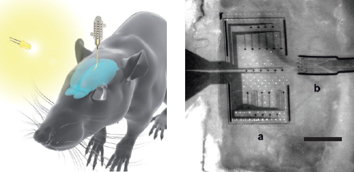
(Left) Representation of the graphene implant placed on the surface of the rat’s brain. (Right) microscope image of a multielectrode array with conventional platinum electrodes (a) vs. the miniature graphene device next to it (b). Scale bar is 1.25 mm. (credit:  Benno M. Blaschke et al./ 2D Mater.)

Neural activity is measured by detecting the electric fields generated when neurons fire. These fields are highly localized, so ultra-small measuring devices that can be densely packed are required for accurate brain readings.

The new device has an microelectrode array of 16 graphene-based transistors arranged on a flexible substrate that can conform to the brain’s surface. Graphene provides biocompatibility, chemical stability, flexibility, and excellent electrical properties, which make it attractive for use in medical devices, especially for brain activity, the researchers suggest.**

(For a state-of-the-art example of microelectrode array use in the brain, see “Brain-computer interface advance allows paralyzed people to type almost as fast as some smartphone users.”)

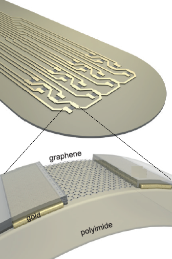
Schematic of the head of a graphene implant showing a graphene transistor array and feed lines. (Inset): cross section of a graphene transistor with graphene between the source and drain contacts, which are covered by an insulating polyimide photoresist. (credit:  Benno M. Blaschke et al./ 2D Mater.)

In an experiment with rats, the researchers used the new devices to record brain activity during sleep and in response to visual light stimulation.

The graphene transistor probes showed good spatial discrimination (identifying specific locations) of the brain activity and outperformed state-of-the-art platinum electrode arrays, with higher signal amplification and a better signal-to-noise performance when scaled down to very small sizes.

That means the graphene transistor probes can be more densely packed and at higher resolution, features that are vital for precision mapping of brain activity. And since the probes have transistor amplifiers built in, they remove the need for the separate pre-amplification required with metal electrodes.

Neural probes are placed directly on the surface of the brain, so safety is important. The researchers determined that the flexible graphene-based probes are non-toxic, did not induce any significant inflammation, and are long-lasting.

“Graphene neural interfaces have shown already a great potential, but we have to improve on the yield and homogeneity of the device production in order to advance towards a real technology,” said Jose Antonio Garrido, who led the research at the Catalan Institute of Nanoscience and Nanotechnology in Spain.

“Once we have demonstrated the proof of concept in animal studies, the next goal will be to work towards the first human clinical trial with graphene devices during intraoperative mapping of the brain. This means addressing all regulatory issues associated to medical devices such as safety, biocompatibility, etc.”

The research was published in the journal 2D Materials.

* With a budget of €1 billion, the Graphene Flagship consortium consists of more than 150 academic and industrial research groups in 23 countries. Launched in 2013, the goal is to take graphene from the realm of academic laboratories into European society within 10 years. The research was a collaborative effort involving Flagship partners Technical University of Munich (TU Munich. Germany), Institut d’Investigacions Biomèdiques August Pi i Sunyer (IDIBAPS, Spain), Spanish National Research Council (CSIC, Spain), The Biomedical Research Networking Center in Bioengineering, Biomaterials and Nanomedicine (CIBER-BBN, Spain) and the Catalan Institute of Nanoscience and Nanotechnology (ICN2, Spain).

** “Using multielectrode arrays for high-density recordings presents important drawbacks. Since the electrode impedance and noise are inversely proportional to the electrode size, a trade-off between spatial resolution and signal-to-noise ratio has to be made. Further, the very small voltages of the recorded signals are highly susceptible to noise in the standard electrode configuration. [That requires preamplification, which means] the fabrication complexity is significantly increased and the additional electrical components required for the voltage-to-current conversion limit the integration density. … Metal-oxide-semiconductor field-effect transistors (MOSFETs) where the gate metal is replaced with an electrolyte and an electrode, referred to as “solution-gated field-effect transistors (SGFETs) or electrolyte-gated field-effect transistors, can be exposed directly to neurons and be used to record action potentials with high fidelity. … Although the potential of graphene-based SGFET technology has been suggested in in vitro studies, so far no in vivo confirmation has been demonstrated. Here we present the fabrication of flexible arrays of graphene SGFETs and demonstrate in vivo mapping of spontaneous slow waves, as well as visually evoked and pre-epileptic activity in the rat.” — Benno M. Blaschke et al./2D Mater.


Abstract of Mapping brain activity with flexible graphene micro-transistors

Establishing a reliable communication interface between the brain and electronic devices is of paramount importance for exploiting the full potential of neural prostheses. Current microelectrode technologies for recording electrical activity, however, evidence important shortcomings, e.g. challenging high density integration. Solution-gated field-effect transistors (SGFETs), on the other hand, could overcome these shortcomings if a suitable transistor material were available. Graphene is particularly attractive due to its biocompatibility, chemical stability, flexibility, low intrinsic electronic noise and high charge carrier mobilities. Here, we report on the use of an array of flexible graphene SGFETs for recording spontaneous slow waves, as well as visually evoked and also pre-epileptic activity in vivo in rats. The flexible array of graphene SGFETs allows mapping brain electrical activity with excellent signal-to-noise ratio (SNR), suggesting that this technology could lay the foundation for a future generation of in vivo recording implants.

Musk launches company to pursue ‘neural lace’ brain-interface technology

image credit | Bloomberg

Elon Musk has launched a California-based company called Neuralink Corp., The Wall Street Journal reported today (Monday, March 27, 2017), citing people familiar with the matter, to pursue “neural lace” brain-interface technology.

Neural lace would help prevent humans from becoming “house cats” to AI, he suggests. “I think one of the solutions that seems maybe the best is to add an AI layer,” Musk hinted at the Code Conference last year. It would be a “digital layer above the cortex that could work well and symbiotically with you.

“We are already a cyborg,” he added. “You have a digital version of yourself online in form of emails and social media. … But the constraint is input/output — we’re I/O bound … particularly output. … Merging with digital intelligence revolves around … some sort of interface with your cortical neurons.”

Reflecting concepts that have been proposed by Ray Kurzweil, “over time I think we will probably see a closer merger of biological intelligence and digital intelligence,” Musk said at the recent World Government Summit in Dubai.

Musk suggested the neural lace interface could be inserted via veins and arteries.

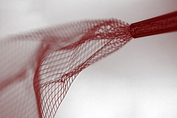
Image showing mesh electronics being injected through sub-100 micrometer inner diameter glass needle into aqueous solution. (credit: Lieber Research Group, Harvard University)

KurzweilAI reported on one approach to a neural-lace-like brain interface in 2015. A “syringe-injectable electronics” concept was invented by researchers in Charles Lieber’s lab at Harvard University and the National Center for Nanoscience and Technology in Beijing. It would involve injecting a biocompatible polymer scaffold mesh with attached microelectronic devices into the brain via syringe.

The process for fabricating the scaffold is similar to that used to etch microchips, and begins with a dissolvable layer deposited on a biocompatible nanoscale polymer mesh substrate, with embedded nanowires, transistors, and other microelectronic devices attached. The mesh is then tightly rolled up, allowing it to be sucked up into a syringe via a thin (100 micrometers internal diameter) glass needle. The mesh can then be injected into brain tissue by the syringe.

The input-output connection of the mesh electronics can be connected to standard electronics devices (for voltage insertion or measurement, for example), allowing the mesh-embedded devices to be individually addressed and used to precisely stimulate or record individual neural activity.

A schematic showing in vivo stereotaxic injection of mesh electronics into a mouse brain (credit: Jia Liu et al./Nature Nanotechnology)

Lieber’s team has demonstrated this in live mice and verified continuous monitoring and recordings of brain signals on 16 channels. “We have shown that mesh electronics with widths more than 30 times the needle ID can be injected and maintain a high yield of active electronic devices … little chronic immunoreactivity,” the researchers said in a June 8, 2015 paper in Nature Nanotechnology. “In the future, our new approach and results could be extended in several directions, including the incorporation of multifunctional electronic devices and/or wireless interfaces to further increase the complexity of the injected electronics.”

This technology would require surgery, but would not have the accessibility limitation of the blood-brain barrier with Musk’s preliminary concept. For direct delivery via the bloodstream, it’s possible that the nanorobots conceived by Robert A. Freitas, Jr. (and extended to interface with the cloud, as Ray Kurzweil has suggested) might be appropriate at some point in the future.

“Neuralink has reportedly already hired several high profile academics in the field of neuroscience: flexible electrodes and nano technology expert  Venessa Tolosa, PhD; UCSF professor Philip Sabes, PhD, who also participated in the Musk-sponsored Beneficial AI conference; and Boston University professor Timothy Gardner, PhD, who studies neural pathways in the brains of songbirds,” Engadget reports.

UPDATE Mar. 28, 2017:


Recode | We are already cyborgs | Elon Musk | Code Conference 2016

A printable, sensor-laden ‘skin’ for robots (or an airplane)

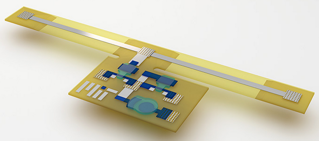
Illustration of 3D-printed sensory composite (credit: Subramanian Sundaram)

MIT researchers have designed a radical new method of creating flexible, printable electronics that combine sensors and processing circuitry.

Covering a robot — or an airplane or a bridge, for example — with sensors will require a technology that is both flexible and cost-effective to manufacture in bulk. To demonstrate the feasibility of their new method, the researchers at MIT’s Computer Science and Artificial Intelligence Laboratory have designed and built a 3D-printed device that responds to mechanical stresses by changing the color of a spot on its surface.

Sensorimotor pathways

“In nature, networks of sensors and interconnects [such as the human nervous system] are called sensorimotor pathways,” says Subramanian Sundaram, an MIT graduate student in electrical engineering and computer science (EECS), who led the project. “We were trying to see whether we could replicate sensorimotor pathways inside a 3-D-printed object. So we considered the simplest organism we could find” — the golden tortoise beetle, or “goldbug,” an insect whose exterior usually appears golden but turns reddish orange if the insect is poked or prodded, that is, mechanically stressed.

The researchers present their new design in the latest issue of the journal Advanced Materials Technologies.

The key innovation was to 3D-print directly on the plastic substrate (support structure) instead of placing components on top. That greatly increases the range of devices that can be created; a printed substrate could consist of many materials, interlocked in intricate but regular patterns, which broadens the range of functional materials that printable electronics can use.*

Printed substrates also open the possibility of devices that, although printed as flat sheets, can fold themselves up into more complex, three-dimensional shapes. Printable robots that spontaneously self-assemble when heated, for instance (see “Self-assembling printable robotic components“), are a  topic of ongoing research at the CSAIL Distributed Robotics Laboratory, led by Daniela Rus, the Andrew and Erna Viterbi Professor of Electrical Engineering and Computer Science at MIT.

3D-printed sensory composite

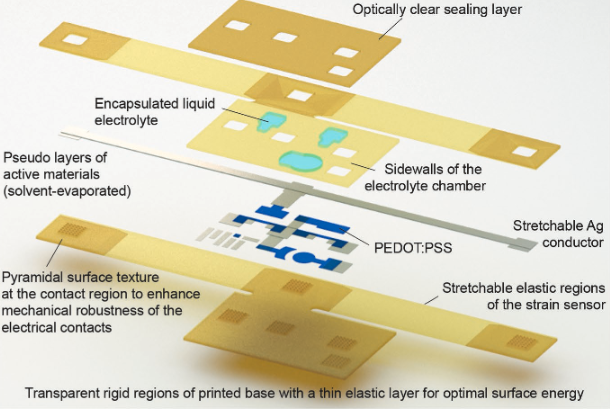
The sensory composite is grouped into 4 sets of functional layers: a base with spatially varying mechanical stiffness and surface energy, electrical materials, electrolyte, and capping layers. All these materials are 3D-printed. (credit: Subramanian Sundaram et al./ Advanced Materials Technologies)

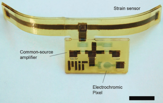
The MIT researchers’ new device is approximately T-shaped, but with a wide, squat base and an elongated crossbar. The crossbar is made from an elastic plastic, with a strip of silver running its length; in the researchers’ experiments, electrodes were connected to the crossbar’s ends. The base of the T is made from a more rigid plastic. It includes two printed transistors and what the researchers call a “pixel,” a circle of semiconducting polymer whose color changes when the crossbars stretch, modifying the electrical resistance of the silver strip.**

A transistor consists of semiconductor channel on top of which sits a “gate,” a metal wire that, when charged, generates an electric field that switches the semiconductor between its electrically conductive and nonconductive states. In a standard transistor, there’s an insulator between the gate and the semiconductor, to prevent the gate current from leaking into the semiconductor channel.

The transistors in the MIT researchers’ device instead separate the gate and the semiconductor with an electrolyte — a layer of water containing  potassium chloride mixed with glycerol. Charging the gate drives potassium ions into the semiconductor, changing its conductivity.***

Photograph of the fully 3D-printed sensory composite shows a strain sensor (top) linked to an electrical amplifier that modulates the transparency of the electrochromic pixel (scale bar is 10mm). (credit: Subramanian Sundaram et al./ Advanced Materials Technologies)

“I am very impressed with both the concept and the realization of the system,” says Hagen Klauk, who leads the Organic Electronic Research Group at the Max Planck Institute for Solid State Research, in Stuttgart, Germany. “The approach of printing an entire optoelectronic system — including the substrate and all the components — by depositing all the materials, including solids and liquids, by 3-D printing is certainly novel, interesting, and useful, and the demonstration of the functional system confirms that the approach is also doable. By fabricating the substrate on the fly, the approach is particularly useful for improvised manufacturing environments where dedicated substrate materials may not be available.”

The work was supported by the DARPA SIMPLEX program through SPAWAR.

* To build the device, the researchers used the MultiFab, a custom 3-D printer developed MIT. The MultiFab already included two different “print heads,” one for emitting hot materials and one for cool, and an array of ultraviolet light-emitting diodes. Using ultraviolet radiation to “cure” fluids deposited by the print heads produces the device’s substrate.

** Sundaram added a copper-and-ceramic heater, which was necessary to deposit the semiconducting plastic: The plastic is suspended in a fluid that’s sprayed onto the device surface, and the heater evaporates the fluid, leaving behind a layer of plastic only 200 nanometers thick. The layer of saltwater lowers the device’s operational voltage, so that it can be powered with an ordinary 1.5-volt battery.

*** But it does render the device less durable. “I think we can probably get it to work stably for two months, maybe,” Sundaram says. “One option is to replace that liquid with something between a solid and a liquid, like a hydrogel, perhaps. But that’s something we would work on later. This is an initial demonstration.”


Abstract of 3D-Printed Autonomous Sensory Composites

A method for 3D-printing autonomous sensory composites requiring no external processing is presented. The composite operates at 1.5 V, locally performs active signal transduction with embedded electrical gain, and responds to stimuli, reversibly transducing mechanical strain into a transparency change. Digital assembly of spatially tailored solids and thin films, with encapsulated liquids, provides a route for realizing complex autonomous systems.

Infrared-light-based Wi-Fi network is 100 times faster

Schematic of a beam of white light being dispersed by a prism into different wavelengths, similar in prinicple to how a new near-infrared WiFi system works (credit: Lucas V. Barbosa/CC)

A new infrared-light WiFi network can provide more than 40 gigabits per second (Gbps) for each user* — about 100 times faster than current WiFi systems — say researchers at Eindhoven University of Technology (TU/e) in the Netherlands.

The TU/e WiFi design was inspired by experimental systems using ceiling LED lights (such as Oregon State University’s experimental WiFiFO, or WiFi Free space Optic, system), which can increase the total per-user speed of WiFi systems and extend the range to multiple rooms, while avoiding interference from neighboring WiFi systems. (However, WiFiFo is limited to 100 Mbps.)

Experimental Oregon State University system uses LED lighting to boost the bandwidth of Wi-Fi systems and extend range (credit: Thinh Nguyen/Oregon State University)

Near-infrared light

Instead of visible light, the TU/e system uses invisible near-infrared light.** Supplied by a fiber optic cable, a few central “light antennas” (mounted on the ceiling, for instance) each use a pair of ”passive diffraction gratings” that radiate light rays of different wavelengths at different angles.

That allows for directing the light beams to specific users. The network tracks the precise location of every wireless device, using a radio signal transmitted in the return direction.***

The TU/e system uses infrared light with a wavelength of 1500 nanometers (a frequency of 200 terahertz, or 40,000 times higher than 5GHz), allowing for significantly increased capacity. The system has so far used the light rays only for downloading; uploads are still done using WiFi radio signals, since much less capacity is usually needed for uploading.

The researchers expect it will take five years or more for the new technology to be commercially available. The first devices to be connected will likely be high-data devices like video monitors, laptops, and tablets.

* That speed is 67 times higher than the current 802.11n WiFi system’s max theoretical speed of 600Mbps capacity — which has to be shared between users, so the ratio is actually about 100 times, according to TU/e researchers. That speed is also 16 times higher than the 2.5 Gbps performance with the best (802.11ac) Wi-Fi system — which also has to be shared (so actually lower) — and in addition, uses the 5GHz wireless band, which has limited range. “The theoretical max speed of 802.11ac is eight 160MHz 256-QAM channels, each of which are capable of 866.7Mbps, for a total of 6,933Mbps, or just shy of 7Gbps,” notes Extreme Tech. “In the real world, thanks to channel contention, you probably won’t get more than two or three 160MHz channels, so the max speed comes down to somewhere between 1.7Gbps and 2.5Gbps. Compare this with 802.11n’s max theoretical speed, which is 600Mbps.”

** The TU/e system was designed by Joanne Oh as a doctoral thesis and part of the wider BROWSE project headed up by professor of broadband communication technology Ton Koonen, with funding from the European Research Council, under the auspices of the noted TU/e Institute for Photonic Integration.

*** According to TU/e researchers, a few other groups are investigating network concepts in which infrared-light rays are directed using movable mirrors. The disadvantage here is that this requires active control of the mirrors and therefore energy, and each mirror is only capable of handling one ray of light at a time. The grating used the and Oh can cope with many rays of light and, therefore, devices at the same time.