WiFi capacity doubled at less than half the size

Columbia University engineering researchers have developed a new “circulator” technology that can double WiFi speed while reducing the size of wireless devices. It does this by requiring only one antenna (instead of two, for transmitter and receiver) and by using conventional CMOS chips instead of resorting to large, expensive magnetic components.
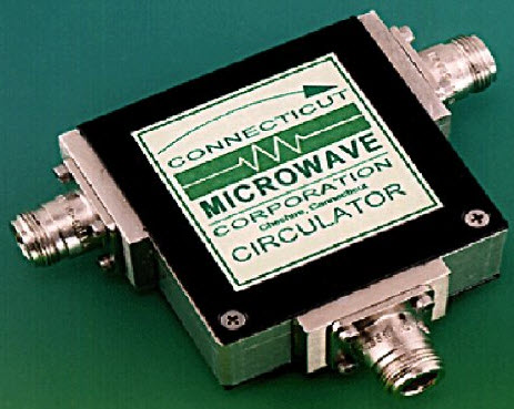
Current bulky circulator design (credit: Connecticut Microwave Corporation)

Columbia engineers previously invented a “full-duplex” radio integrated circuit on a conventional CMOS chip. “Full duplex” means simultaneous transmission and reception at the same frequency in a wireless radio, unlike “half-duplex” (transmitting and receiving at different times, used by current cell phones and other wireless devices). Full duplex also allows for faster transmission speeds.

The new circulator technology further miniaturizes future WiFi and other wireless devices (see Lighter, cheaper radio-wave device could double the useful bandwidth in wireless communications — an earlier circulator device developed by The University of Texas at Austin engineers that was not integrated on a CMOS chip).

“Full-duplex communications, where the transmitter and the receiver operate at the same time and at the same frequency, has become a critical research area and now we’ve shown that WiFi capacity can be doubled on a nanoscale silicon chip with a single antenna,” said Electrical Engineering Associate Professor Harish Krishnaswamy, director of the Columbia High-Speed and Mm-wave IC (CoSMIC) Lab. “This has enormous implications for devices like smartphones and tablets.”
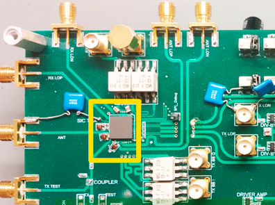
Prototype of first CMOS full-duplex receiver IC with integrated magnetic-free circulator (credit: Negar Reiskarimian, Columbia Engineering)

By combining circulator and full-duplex technologies, “this technology could revolutionize the field of telecommunications,” he said. “Our circulator is the first to be put on a silicon chip, and we get literally orders of magnitude better performance than prior work.”

How to embed circulator technology on a CMOS chip
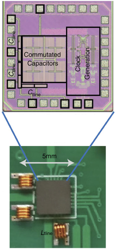
CMOS circulator IC on a printed-curcuit board, interfaced with off-chip inductors. (credit: Negar Reiskarimian, Columbia Engineering)

A circulator allows for using only one antenna to both transmit and receive. To do that, it has to “break” “Lorentz reciprocity” — a fundamental physical characteristic of most electronic structures that requires that electromagnetic waves travel in the same manner in both forward and reverse directions.

The traditional way of breaking Lorentz reciprocity and building radio-frequency circulators has been to use magnetic materials such as ferrites, which lose reciprocity when an external magnetic field is applied. But these materials are not compatible with silicon chip technology, and ferrite circulators are bulky and expensive.

Krishnaswamy and his team were able to design a highly miniaturized circulator that uses switches to rotate the signal across a set of capacitors to emulate the non-reciprocal “twist” of the signal that is seen in ferrite materials.

“Being able to put the circulator on the same chip as the rest of the radio has the potential to significantly reduce the size of the system, enhance its performance, and introduce new functionalities critical to full duplex,” says PhD student Jin Zhou, who integrated the circulator with a full-duplex receiver.

Circulator circuits and components have applications in many different scenarios, from radio-frequency full-duplex communications and radar to building isolators that prevent high-power transmitters from being damaged by back-reflections from the antenna. The ability to break reciprocity also opens up new possibilities in radio-frequency signal processing that are yet to be discovered.

The circulator research is published in an open-access paper on April 15 in Nature Communications. A paper detailing the single-chip full-duplex radio with the circulator and additional echo cancellation was presented at the 2016 IEEE International Solid-State Circuits Conference on February 2.

The work has been funded by the DARPA Microsystems Technology Office and the National Science Foundation.


Abstract of Magnetic-free non-reciprocity based on staggered commutation

Lorentz reciprocity is a fundamental characteristic of the vast majority of electronic and photonic structures. However, non-reciprocal components such as isolators, circulators and gyrators enable new applications ranging from radio frequencies to optical frequencies, including full-duplex wireless communication and on-chip all-optical information processing. Such components today dominantly rely on the phenomenon of Faraday rotation in magneto-optic materials. However, they are typically bulky, expensive and not suitable for insertion in a conventional integrated circuit. Here we demonstrate magnetic-free linear passive non-reciprocity based on the concept of staggered commutation. Commutation is a form of parametric modulation with very high modulation ratio. We observe that staggered commutation enables time-reversal symmetry breaking within very small dimensions (λ/1,250 × λ/1,250 in our device), resulting in a miniature radio-frequency circulator that exhibits reduced implementation complexity, very low loss, strong non-reciprocity, significantly enhanced linearity and real-time reconfigurability, and is integrated in a conventional complementary metal–oxide–semiconductor integrated circuit for the first time.


Abstract of Receiver with integrated magnetic-free N-path-filter-based non-reciprocal circulator and baseband self-interference cancellation for full-duplex wireless

Full-duplex (FD) is an emergent wireless communication paradigm where the transmitter (TX) and the receiver (RX) operate at the same time and at the same frequency. The fundamental challenge with FD is the tremendous amount of TX self-interference (SI) at the RX. Low-power applications relax FD system requirements [1], but an FD system with -6dBm transmit power, 10MHz signal bandwidth and 12dB NF budget still requires 86dB of SI suppression to reach the -92dBm noise floor. Recent research has focused on techniques for integrated self-interference cancellation (SIC) in FD receivers [1-3]. Open challenges include achieving the challenging levels of SIC through multi-domain cancellation, and low-loss shared-antenna (ANT) interfaces with high TX-to-RX isolation. Sharedantenna interfaces enable compact form factor, translate easily to MIMO, and ease system design through channel reciprocity.

IBM makes quantum computing available free on IBM Cloud

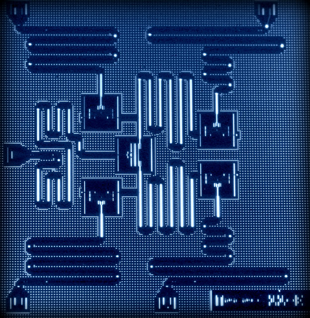
Layout of IBM’s five superconducting quantum bit device. In 2015, IBM scientists demonstrated critical breakthroughs to detect quantum errors by combining superconducting qubits in latticed arrangements, and whose quantum circuit design is the only physical architecture that can scale to larger dimensions. Now, IBM scientists have achieved a further advance by combining five qubits in the lattice architecture, which demonstrates a key operation known as a parity measurement — the basis of many quantum error correction protocols. (credit: IBM Research)

IBM Research has announced that effective Wednesday May 4, it is making quantum computing available free to members of the public, who can access and run experiments on IBM’s quantum processor, via the IBM Cloud, from any desktop or mobile device.

IBM believes quantum computing is the future of computing and has the potential to solve certain problems that are impossible to solve on today’s supercomputers.

The cloud-enabled quantum computing platform, called IBM Quantum Experience, will allow users to run algorithms and experiments on IBM’s quantum processor, work with the individual quantum bits (qubits), and explore tutorials and simulations around what might be possible with quantum computing.

The quantum processor is composed of five superconducting qubits and is housed at the IBM T.J. Watson Research Center in New York. IBM’s quantum architecture can scale to larger quantum systems. It is aimed at building a universal quantum computer that can be programmed to perform any computing task and will be exponentially faster than classical computers for a number of important applications for science and business, IBM says.


IBM | Explore our 360 Video of the IBM Research Quantum Lab

IBM envisions medium-sized quantum processors of 50–100 qubits to be possible in the next decade. With a quantum computer built of just 50 qubits, none of today’s TOP500 supercomputers could successfully emulate it, reflecting the tremendous potential of this technology.

“Quantum computing is becoming a reality and it will extend computation far beyond what is imaginable with today’s computers,” said Arvind Krishna, senior vice president and director, IBM Research. “This moment represents the birth of quantum cloud computing. By giving hands-on access to IBM’s experimental quantum systems, the IBM Quantum Experience will make it easier for researchers and the scientific community to accelerate innovations in the quantum field, and help discover new applications for this technology.”

This leap forward in computing could lead to the discovery of new pharmaceutical drugs and completely safeguard cloud computing systems, IBM believes. It could also unlock new facets of artificial intelligence (which could lead to future, more powerful Watson technologies), develop new materials science to transform industries, and search large volumes of big data.

The IBM Quantum Experience


IBM | Running an experiment in the IBM Quantum Experience

Coupled with software expertise from the IBM Research ecosystem, the team has built a dynamic user interface on the IBM Cloud platform that allows users to easily connect to the quantum hardware via the cloud.

In the future, users will have the opportunity to contribute and review their results in the community hosted on the IBM Quantum Experience and IBM scientists will be directly engaged to offer more research and insights on new advances. IBM plans to add more qubits and different processor arrangements to the IBM Quantum Experience over time, so users can expand their experiments and help uncover new applications for the technology.

IBM employs superconducting qubits that are made with superconducting metals on a silicon chip and can be designed and manufactured using standard silicon fabrication techniques. Last year, IBM scientists demonstrated critical breakthroughs to detect quantum errors by combining superconducting qubits in latticed arrangements, and whose quantum circuit design is the only physical architecture that can scale to larger dimensions.


IBM | IBM Brings Quantum Computing to the Cloud

Now, IBM scientists have achieved a further advance by combining five qubits in the lattice architecture, which demonstrates a key operation known as a parity measurement — the basis of many quantum error correction protocols.

By giving users access to IBM’s experimental quantum systems, IBM believes it will help businesses and organizations begin to understand the technology’s potential, for universities to grow their teaching programs in quantum computing and related subjects, and for students (IBM’s potential future customers) to become aware of promising new career paths. And of course, to raise IBM’s marketing profile in this emerging field.

You’ll interact with smartphones and smartwatches by writing/gesturing on any surface, using sonar signals

FingerIO lets you interact with mobile devices by writing or gesturing on any nearby surface, turning a smartphone or smartwatch into an active sonar device (credit: Dennis Wise, University of Washington)

A new sonar technology called FingerIO will make it easier to interact with screens on smartwatches and smartphones by simply writing or gesturing on any nearby surface. It’s is an active sonar system using the device’s own microphones and speakers to track fine-grained finger movements (to within 8mm).

Because sound waves travel through fabric and do not require line of sight, users can even interact with these devices (including writing text) inside a front pocket or a smartwatch hidden under a sweater sleeve.


University of Washington Computer Science & Engineering | FingerIO

Developed by University of Washington computer scientists and electrical engineers, FingerIO uses the device’s own speaker to emit an inaudible ultrasonic wave. That signal bounces off the finger, and those “echoes” are recorded by the device’s microphones and used to calculate the finger’s location in space.

Using sound waves to track finger motion offers several advantages over cameras — which don’t work without line-of-sight or when the device is hidden by fabric or another obstructions — and other technologies like radar that require both custom sensor hardware and greater computing power, said senior author and UW assistant professor of computer science and engineering Shyam Gollakota.

But standard sonar echoes are weak and typically not accurate enough to track finger motion at high resolution. Errors of a few centimeters would make it impossible to differentiate between writing individual letters or subtle hand gestures.

So the UW researchers used “Orthogonal Frequency Division Multiplexing” (used in cellular telecommunications and WiFi), allowing for tracking phase changes in the echoes and correcting for any errors in the finger location.

Applications of fingerIO. a) Transform any surface into a writing interface; b) provide a new interface for smartwatch form factor devices; c) enable gesture interaction with a phone in a pocket; d) work even when the watch is occluded. (credit: R. Nandakumar et al.)

Two microphones are needed to track finger motion in two dimensions, and three for three dimensions. So this system may work (when available commercially*) with some smartphones (it was tested with a Samsung Galaxy S4), but today’s smartwatches typically only have one microphone.

Next steps for the research team include demonstrating how FingerIO can be used to track multiple fingers moving at the same time, and extending its tracking abilities into three dimensions by adding additional microphones to the devices.

The research was funded by the National Science Foundation and Google and will be described in a paper to be presented in May at the Association for Computing Machinery’s CHI 2016 conference in San Jose, California.

* Hint: Microsoft Research principal researcher Desney Tan is a co-author.


editor’s comments: This tech will be great for students and journalists taking notes and for controlling music and videos. It could also help prevent robberies. How would you use it?


Abstract of FingerIO: Using Active Sonar for Fine-Grained Finger Tracking

We present fingerIO, a novel fine-grained finger tracking solution for around-device interaction. FingerIO does not require instrumenting the finger with sensors and works even in the presence of occlusions between the finger and the device. We achieve this by transforming the device into an active sonar system that transmits inaudible sound signals and tracks the echoes of the finger at its microphones. To achieve subcentimeter level tracking accuracies, we present an innovative approach that use a modulation technique commonly used in wireless communication called Orthogonal Frequency Division Multiplexing (OFDM). Our evaluation shows that fingerIO can achieve 2-D finger tracking with an average accuracy of 8 mm using the in-built microphones and speaker of a Samsung Galaxy S4. It also tracks subtle finger motion around the device, even when the phone is inside a pocket. Finally, we prototype a smart watch form-factor fingerIO device and show that it can extend the interaction space to a 0.5×0.25 m2 region on either side of the device and work even when it is fully occluded from the finger.

New ‘machine unlearning’ technique deletes unwanted data

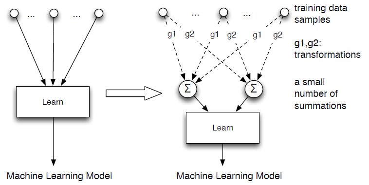
The novel approach to making systems forget data is called “machine unlearning” by the two researchers who are pioneering the concept. Instead of making a model directly depend on each training data sample (left), they convert the learning algorithm into a summation form (right) – a process that is much easier and faster than retraining the system from scratch. (credit: Yinzhi Cao and Junfeng Yang)

Machine learning systems are becoming ubiquitous, but what about false or damaging information about you (and others) that these systems have learned? Is it even possible for that information to be ever corrected? There are some heavy security and privacy questions here. Ever Google yourself?

Some background: machine-learning software programs calculate predictive relationships from massive amounts of data. The systems identify these predictive relationships using advanced algorithms — a set of rules for solving math problems — and “training data.” This data is then used to construct the models and features that enable a system to predict things, like the probability of rain next week or when the Zika virus will arrive in your town.

This intricate process means that a piece of raw data often goes through a series of computations in a system. The computations and information derived by the system from that data together form a complex propagation network called the data’s “lineage” (a term coined by Yinzhi Cao, a Lehigh University assistant professor of computer science and engineering, and his colleague, Junfeng Yang of Columbia University).

“Effective forgetting systems must be able to let users specify the data to forget with different levels of granularity,” said Cao. “These systems must remove the data and undo its effects so that all future operations run as if the data never existed.”

Widely used learning systems such as Google Search are, for the most part, only able to forget a user’s raw data upon request — not the data’s lineage (what the user’s data connects to). However, in October 2014, Google removed more than 170,000 links to comply with the ruling, which affirmed users’ right to control what appears when their names are searched. In July 2015, Google said it had received more than a quarter-million such requests.

How “machine unlearning” works

Now the two researchers say they have developed a way to forget faster and more effectively. Their concept, called “machine unlearning,” led to a four-year, $1.2 million National Science Foundation grant to develop the approach.

Building on work that was presented at a 2015 IEEE Symposium and then published, Cao and Yang’s “machine unlearning” method is based on the assumption that most learning systems can be converted into a form that can be updated incrementally without costly retraining from scratch.

Their approach introduces a layer of a small number of summations between the learning algorithm and the training data to eliminate dependency on each other. That means the learning algorithms depend only on the summations and not on individual data.

Using this method, unlearning a piece of data and its lineage no longer requires rebuilding the models and features that predict relationships between pieces of data. Simply recomputing a small number of summations would remove the data and its lineage completely — and much faster than through retraining the system from scratch, the researchers claim.

Verification?

Cao and Yang tested their unlearning approach on four diverse, real-world systems: LensKit, an open-source recommendation system; Zozzle, a closed-source JavaScript malware detector; an open-source OSN spam filter; and PJScan, an open-source PDF malware detector.

Cao and Yang are now adapting the technique to other systems and creating verifiable machine unlearning to statistically test whether unlearning has indeed repaired a system or completely wiped out unwanted data.

“We foresee easy adoption of forgetting systems because they benefit both users and service providers,” they said. “With the flexibility to request that systems forget data, users have more control over their data, so they are more willing to share data with the systems.”

The researchers envision “forgetting systems playing a crucial role in emerging data markets where users trade data for money, services, or other data, because the mechanism of forgetting enables a user to cleanly cancel a data transaction or rent out the use rights of her data without giving up the ownership.”


editor’s comments: I’d like to see case studies and critical reviews of this software by independent security and privacy experts. Yes, I’m paranoid but… etc. Your suggestions? To be continued…


Abstract of Towards Making Systems Forget with Machine Unlearning

Today’s systems produce a rapidly exploding amount of data, and the data further derives more data, forming a complex data propagation network that we call the data’s lineage. There are many reasons that users want systems to forget certain data including its lineage. From a privacy perspective, users who become concerned with new privacy risks of a system often want the system to forget their data and lineage. From a security perspective, if an attacker pollutes an anomaly detector by injecting manually crafted data into the training data set, the detector must forget the injected data to regain security. From a usability perspective, a user can remove noise and incorrect entries so that a recommendation engine gives useful recommendations. Therefore, we envision forgetting systems, capable of forgetting certain data and their lineages, completely and quickly. This paper focuses on making learning systems forget, the process of which we call machine unlearning, or simply unlearning. We present a general, efficient unlearning approach by transforming learning algorithms used by a system into a summation form. To forget a training data sample, our approach simply updates a small number of summations — asymptotically faster than retraining from scratch. Our approach is general, because the summation form is from the statistical query learning in which many machine learning algorithms can be implemented. Our approach also applies to all stages of machine learning, including feature selection and modeling. Our evaluation, on four diverse learning systems and real-world workloads, shows that our approach is general, effective, fast, and easy to use.

New electronic stethoscope and app diagnose lung conditions

1. Electronic stethoscope records patient’s breathing. Lung sounds are sent to a phone or tablet and analyzed by an app. 3. Medical professionals can listen and see the results in real time from any location to diagnose the patient. (credit: Hiroshima University)

The traditional stethoscope has just been superseded by an electronic stethoscope and an app called Respiratory Sounds Visualizer, which can automatically classify lung sounds into five common diagnostic categories.* The system was developed by three physician researchers at Hiroshima University and Fukushima Medical University in collaboration with Pioneer Corporation.

The respiratory specialist doctors recorded and classified lung sounds of 878 patients, then turned these diagnoses into templates to create a mathematical formula that evaluates the length, frequency, and intensity of lung sounds. The resulting app can recognize the sound patterns consistent with five different respiratory diagnoses.

How the Respiratory Sounds Visualizer app works

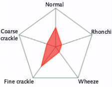
Based on an analysis of the characteristics of respiratory sounds, the Respiratory Sounds Visualizer app generates this diagnostic chart. The total area in red represents the overall volume of sound, and the proportion of red around each line from the center to each vertex represents the proportion of the overall sound that each respiratory sound contributes. (credit: Shinichiro Ohshimo et al./Annals of Internal Medicine)

The app analyzes the lung sounds and maps them on a five-sided chart. Each of the five axes represents one of the five types of lung sounds. Doctors and patients can see the likely diagnosis based on the length of the axis covered in red.

A doctor working in less-than-ideal circumstances, such as a noisy emergency room or field hospital, could rely on the computer program to “hear” what they might otherwise miss, and the new system could help student doctors learn.

The results from the computer program are simple to interpret and can be saved and shared electronically. In the future, this convenience may allow patients to track and record their own lung function during chronic conditions, like chronic obstructive pulmonary disease (COPD) or cystic fibrosis.

“We plan to use the electronic stethoscope and Respiratory Sounds Visualizer with our own patients after further improving [the mathematical calculations]. We will also release the computer program as a downloadable application to the public in the near future,” said Shinichiro Ohshimo, MD, PhD, an emergency physician in the Department of Emergency and Critical Care Medicine at Hiroshima University Hospital and one of the researchers involved in developing the technology.

* Despite advances in technology, respiratory physiology still depends primarily on chest auscultation, [which is] subjective and requires sufficient training. In addition, identification of the five respiratory sounds specified by the International Lung Sounds Association is difficult because their frequencies overlap:The frequency of normal respiratory sound is 100 to 1000 Hz, wheeze is 100 to 5000 Hz, rhonchus is 150 Hz, coarse crackle is 350 Hz, and fine crackle is 650 Hz. — Shinichiro Ohshimo et al./Annals of Internal Medicine.

A ‘magic wand’ to simplify network setup and improve security

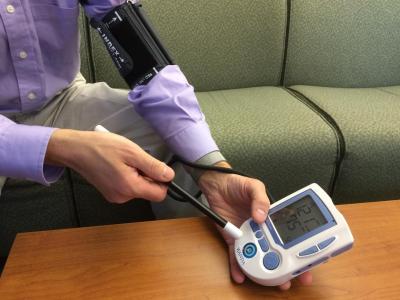
Dartmouth College Professor David Kotz demonstrates a commercial prototype of “Wanda” imparting information such as the network name and password of a WiFi access point onto a blood pressure monitor (credit: Dartmouth College)

Ever just want to wave a magic wand instead of dealing with a complex home network setup?

Well, Dartmouth College computer science professor David Kotz has figured out how to do just that. Called “Wanda,” it’s a small rod that makes it simple to link a new device (such as a blood-pressure meter or smartphone) to a WiFi network by just pointing the rod at the device.

The system is part of a National Science Foundation-funded project led by Dartmouth called “Trustworthy Health and Wellness” aimed at protecting patients and their confidentiality as medical records move from paper to electronic form and as health care increasingly moves out of doctors’ offices and hospitals and into the home.

Kotz says wireless and mobile health technologies have great potential to improve quality and access to care, reduce costs and improve health, “but these new technologies, whether in the form of software for smartphones or specialized devices to be worn, carried or applied as needed, also pose risks if they’re not designed or configured with security and privacy in mind.”

Setting up a secure network at home

Most people don’t know how to set up and maintain a secure network in their home, which can lead to compromised or stolen data or potentially allow hackers access to critical devices such as heart rate monitors or dialysis machines.

There are three basic operations when bringing a new mobile device into the home, workplace or clinic: configure the device to join the wireless local-area network (such as enter a Wi-Fi SSID and password); partner the device with other nearby devices so they can work together; and configure the device so it connects to the relevant individual or organizational account in the cloud.

“Wanda” is a small hardware device with two antennas. To add a new device to their home (or clinic) Wi-Fi network, users simply pull the wand from a USB port on the Wi-Fi access point, carry it close to the new device, and point it at the device. Within a few seconds, the wand securely beams the secret Wi-Fi network information to the device.*

The same method can be used to transfer any information from the wand to the new device without anyone nearby capturing the secrets or tampering with the information.

Kotz says the technology could be useful for a wide range of device management tasks and in a wide variety of applications in addition to healthcare.

Supported by a $10-million, five-year grant from the NSF’s Secure and Trustworthy Cyberspace program, the Frontier-scale project includes experts in computer science, business, behavioral health, health policy and healthcare information technology at Dartmouth College, Johns Hopkins University, the University of Illinois Urbana-Champaign (UIUC), the University of Michigan and Vanderbilt University.

Wanda will be presented at the IEEE International Conference on Computer Communications in April.

* Wanda builds on pioneering work done by Cai et al. in  “Good neighbor: Ad hoc pairing of nearby wireless devices by multiple antennas” in NDSS, 2011). It determines when it is in close proximity to another transmitting device by measuring the difference in received  signal  strength on the  two antennas.


Abstract of Wanda: securely introducing mobile devices

Nearly every setting is increasingly populated with wireless and mobile devices – whether appliances in a home, medical devices in a health clinic, sensors in an industrial setting, or devices in an office or school. There are three fundamental operations when bringing a new device into any of these settings: (1) to configure the device to join the wireless local-area network, (2) to partner the device with other nearby devices so they can work together, and (3) to configure the device so it connects to the relevant individual or organizational account in the cloud. The challenge is to accomplish all three goals simply, securely, and consistent with user intent. We present a novel approach we call Wanda – a ‘magic wand’ that accomplishes all three of the above goals – and evaluate a prototype implementation.

‘Eternal 5D’ data storage could reliably record the history of humankind

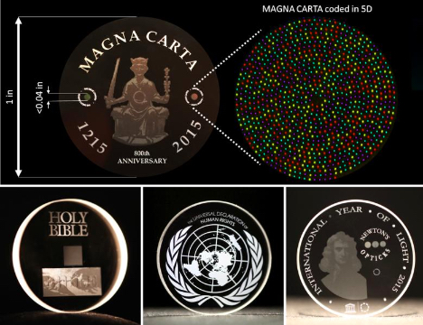
Documents captured in nanostructured glass, expected to last billions of years (credit: University of Southampton)

Scientists at the University of Southampton Optoelectronics Research Centre (ORC) have developed the first digital data storage system capable of creating archives that can survive for billions of years.

Using nanostructured glass, the system has 360 TB per disc capacity, thermal stability up to 1,000°C, and virtually unlimited lifetime at room temperature (or 13.8 billion years at 190°C ).

As a “highly stable and safe form of portable memory,” the technology opens up a new era of “eternal” data archiving that could be essential to cope with the accelerating amount of information currently being created and stored, the scientists says.* The system could be especially useful for organizations with big archives, such as national archives, museums, and libraries, according to the scientists.

Superman memory crystal

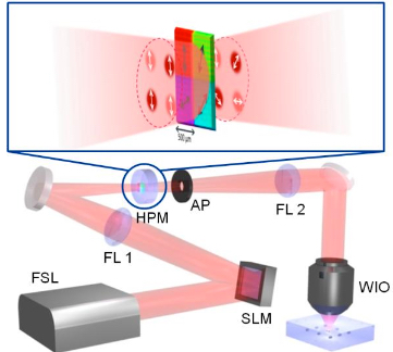
5D optical storage writing setup. FSL: femtosecond laser; SLM: spatial light modulator; FL1 and FL2: Fourier lens; HPM: half-wave plate matrix; AP: aperture; WIO: water immersion objective. Inset: Linearly polarized light (white arrows) with different intensity levels propagate simultaneously through each half-wave plate segment with different slow-axis orientation (black arrows). The colors of the rectangle indicate four different intensity levels. (credit: University of Southampton)

The recording system uses an ultrafast laser to produce extremely short (femtosecond) and intense pulses of light. The file is written in three up to 18 layers of nanostructured dots separated by five micrometers (one millionth of a meter) in fuzed quartz (coined as a “Superman memory crystal” (as in “memory crystals” used in the Superman films).” The self-assembled nanostructures change the way light travels through glass, modifying the polarization of light, which can then be read by a combination optical microscope and polarizer, similar to that found in Polaroid sunglasses.

The recording method is described as “5D” because the information encoding is in five dimensions — three-dimensional position plus size and orientation.

So far, the researchers have saved major documents from human history, such as the Universal Declaration of Human Rights (UDHR), Newton’s Opticks, Magna Carta, and Kings James Bible as digital copies. A copy of the UDHR encoded to 5D data storage was recently presented to UNESCO by the ORC at the International Year of Light (IYL) closing ceremony in Mexico.

The team is now looking for industry partners to further develop and commercialize this technology.

The researchers will present their research at the photonics industry’s SPIE (the International Society for Optical Engineering Conference) in San Francisco on Wednesday Feb. 17.

* In 2008, the International Data Corporation [found] that total capacity of data stored is increasing by around 60% each year. As a result, more than 39,000 exabytes of data will be generated by 2020. This amount of data will cause a series of problems and one of the main will be power consumption. 1.5% of the total U.S. electricity consumption in 2010 was given to the data centers in the U.S. According to a report by the Natural Resources Defence Council, the power consumption of all data centers in the U.S. will reach roughly 140 billion kilowatt-hours per each year by 2020. This amount of electricity is equivalent to that generated by roughly thirteen Heysham 2 nuclear power stations (one of the biggest stations in UK, net 1240 MWe).

Most of these data centers are built based on hard-disk drive (HDD), with only a few designed on optical discs. HDD is the most popular solution for digital data storage according to the International Data Corporation. However, HDD is not an energy-efficient option for data archiving; the loading energy consumption is around 0.04 W/GB. In addition, HDD is an unsatisfactory candidate for long-term storage due to the short lifetime of the hardware and requires transferring data every two years to avoid any loss.

— Jingyu Zhang et al. Eternal 5D data storage by ultrafast laser writing in glass. Proceedings of the SPIE OPTO 2016


Abstract of Eternal 5D data storage by ultrafast laser writing in glass

Femtosecond laser writing in transparent materials has attracted considerable interest due to new science and a wide range of applications from laser surgery, 3D integrated optics and optofluidics to geometrical phase optics and ultra-stable optical data storage. A decade ago it has been discovered that under certain irradiation conditions self-organized subwavelength structures with record small features of 20 nm, could be created in the volume of silica glass. On the macroscopic scale the self-assembled nanostructure behaves as a uniaxial optical crystal with negative birefringence. The optical anisotropy, which results from the alignment of nano-platelets, referred to as form birefringence, is of the same order of magnitude as positive birefringence in crystalline quartz. The two independent parameters describing birefringence, the slow axis orientation (4th dimension) and the strength of retardance (5th dimension), are explored for the optical encoding of information in addition to three spatial coordinates. The slow axis orientation and the retardance are independently manipulated by the polarization and intensity of the femtosecond laser beam. The data optically encoded into five dimensions is successfully retrieved by quantitative birefringence measurements. The storage allows unprecedented parameters including hundreds of terabytes per disc data capacity and thermal stability up to 1000°. Even at elevated temperatures of 160oC, the extrapolated decay time of nanogratings is comparable with the age of the Universe – 13.8 billion years. The demonstrated recording of the digital documents, which will survive the human race, including the eternal copies of Kings James Bible and Magna Carta, is a vital step towards an eternal archive.

NASA engineers to build first integrated-photonics modem

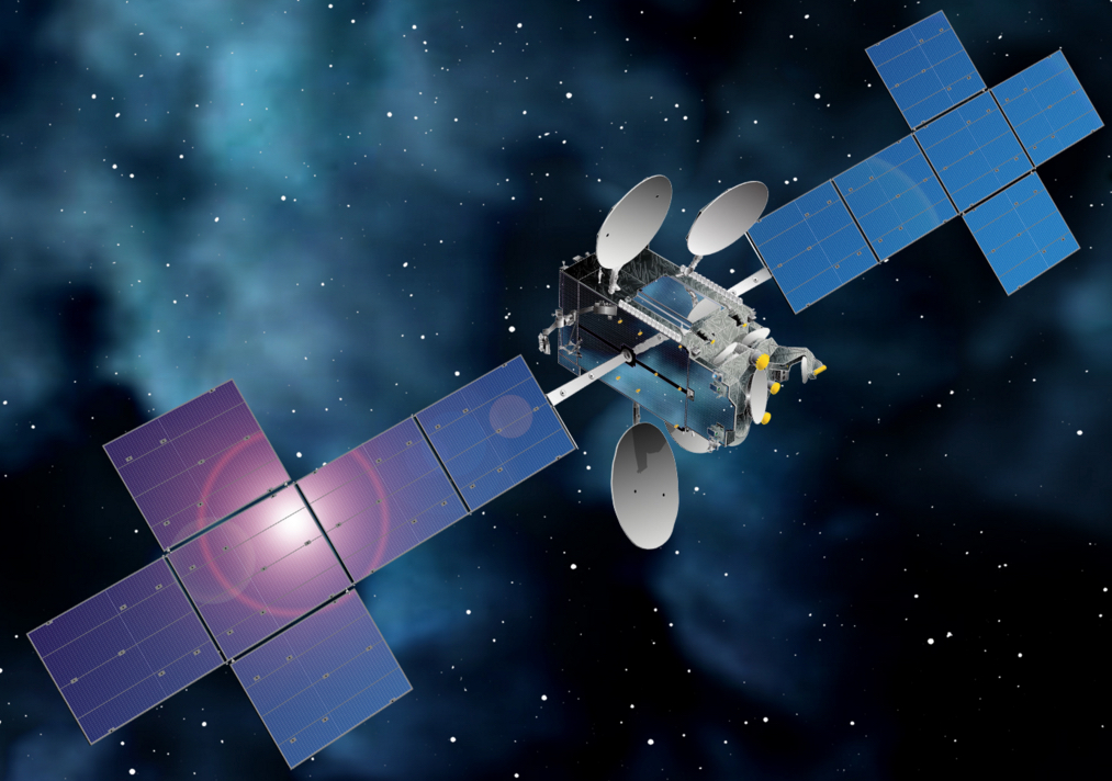
NASA laser expert Mike Krainak and his team plan to replace portions of this fiber-optic receiver with an integrated-photonic circuit (its size will be similar to the chip he is holding) and will test the advanced modem on the International Space Station. (credit: W. Hrybyk/NASA)

A NASA team plans to build the first integrated-photonics modem, using an emerging, potentially revolutionary technology that could transform everything from telecommunications, medical imaging, advanced manufacturing to national defense.

The cell phone-sized device incorporates optics-based functions, such as lasers, switches, and fiber-optic wires, onto a microchip similar to an integrated circuit found in all electronics hardware.

The device will be tested aboard the International Space Station beginning in 2020 as part of NASA’s multi-year Laser Communications Relay Demonstration (LCRD). The Integrated LCRD LEO (Low-Earth Orbit) User Modem and Amplifier (ILLUMA) will serve as a low-Earth-orbit terminal for NASA’s LCRD, demonstrating another capability for high-speed, laser-based communications.

Space communications requires 100 times higher data rates

Since its inception in 1958, NASA has relied exclusively on radio frequency (RF)-based communications. Today, with missions demanding higher data rates than ever before, the need for LCRD has become more critical, said Don Cornwell, director of NASA’s Advanced Communication and Navigation Division within the space Communications and Navigation Program, which is funding the modem’s development.

LCRD, expected to begin operations in 2019, promises to transform the way NASA sends and receives data, video and other information. It will use lasers to encode and transmit data at rates 10 to 100 times faster than today’s communications equipment, requiring significantly less mass and power.

Such a leap in technology could deliver video and high-resolution measurements from spacecraft over planets across the solar system — permitting researchers to make detailed studies of conditions on other worlds, much as scientists today track hurricanes and other climate and environmental changes here on Earth.

A payload aboard the Lunar Atmosphere and Dust Environment Explorer (LADEE) demonstrated record-breaking download and upload speeds to and from lunar orbit at 622 megabits per second (Mbps) and 20 Mbps, respectively, in 2013 (see “NASA laser communication system sets record with data transmissions to and from Moon“).

LCRD, however, is designed to be an operational system after an initial two-year demonstration period. It involves a hosted payload and two specially equipped ground stations. The mission will dedicate the first two years to demonstrating a fully operational system, from geosynchronous orbit to ground stations. NASA then plans to use ILLUMA to test communications between geosynchronous and low-Earth-orbit spacecraft, Cornwell said.

Laser Communications Relay Demonstration (LCRD), artist’s illustration (credit: NASA)

Integrated photonics: transforming light-based technologies

ILLUMA incorporates an emerging technology — integrated photonics — that is expected to transform any technology that employs light. This includes everything from Internet communications over fiber optic cable to spectrometers, chemical detectors, and surveillance systems.

“Integrated photonics are like an integrated circuit, except they use light rather than electrons to perform a wide variety of optical functions,” Cornwell said. Recent developments in nanostructures, metamaterials, and silicon technologies have expanded the range of applications for these highly integrated optical chips. Furthermore, they could be lithographically printed in mass — just like electronic circuitry today — further driving down the costs of photonic devices.

“The technology will simplify optical system design, said Mike Krainak, who is leading the modem’s development at NASA’s Goddard Space Flight Center in Greenbelt, Maryland. “It will reduce the size and power consumption of optical devices, and improve reliability, all while enabling new functions from a lower-cost system.”

Krainak also serves as NASA’s representative on the country’s first consortium to advance integrated photonics. Funded by the U.S. Department of Defense, the non-profit American Institute for Manufacturing Integrated Photonics, with headquarters in Rochester, New York, brings together the nation’s leading technological talent to establish global leadership in integrated photonics. Its primary goal is developing low-cost, high-volume, manufacturing methods to merge electronic integrated circuits with integrated photonic devices.

NASA’s Space Technology Mission Directorate (STMD) also appointed Krainak as the integrated photonics lead for its Space Technology Research Grants Program, which supports early-stage innovations. The program recently announced a number of research awards under this technology area (see related story).

Photonics on a chip

Under the NASA project, Krainak and his team will reduce the size of the terminal, now about the size of two toaster ovens — a challenge made easier because all light-related functions will be squeezed onto a microchip. Although the modem is expected to use some optic fiber, ILLUMA is the first step in building and demonstrating an integrated photonics circuit that ultimately will embed these functions onto a chip, he said.

ILLUMA will flight-qualify the technology, as well as demonstrate a key capability for future spacecraft. In addition to communicating to ground stations, future satellites will require the ability to communicate with one another, he said.

“What we want to do is provide a faster exchange of data to the scientific community. Modems have to be inexpensive. They have to be small. We also have to keep their weight down,” Krainak said. The goal is to develop and demonstrate the technology and then make it available to industry and other government agencies, creating an economy of scale that will further drive down costs. “This is the payoff,” he said.

Although integrated photonics promises to revolutionize space-based science and inter-planetary communications, its impact on terrestrial uses also is equally profound, Krainak added. One such use is with data centers. These costly, very large facilities house servers that are connected by fiber optic cable to store, manage and distribute data.

Integrated photonics promises to dramatically reduce the need for and size of these behemoths — particularly since the optic hardware needed to operate these facilities will be printed onto a chip, much like electronic circuitry today. In addition to driving down costs, the technology promises faster computing power.

“Google, Facebook, they’re all starting to look at this technology,” Krainak said. “As integrated photonics progresses to be more cost effective than fiber optics, it will be used,” Krainak said. “Everything is headed this way.”


NASA | Laser Comm: That’s a Bright Idea

AI will replace smartphones within 5 years, Ericsson survey suggests

(credit: Ericsson ConsumerLab)

Artificial intelligence (AI) interfaces will take over, replacing smartphones in five years, according to a survey of more than 5000 smartphone customers in nine countries by Ericsson ConsumerLab in the fifth edition of its annual trend report, 10 Hot Consumer Trends 2016 (and beyond).

Smartphone users believe AI will take over many common activities, such as searching the net, getting travel guidance, and as personal assistants. The survey found that 44 percent think an AI system would be as good as a teacher and one third would like an AI interface to keep them company. A third would rather trust the fidelity of an AI interface than a human for sensitive matters; and 29 percent agree they would feel more comfortable discussing their medical condition with an AI system.

However, many of the users surveyed find smartphones limited.

Impractical. Constantly having a screen in the palm of your hand is not always a practical solution, such as in driving or cooking.

Battery capacity limits. One in 3 smartphone users want a 7−8 inch screen, creating a battery drain vs. size and weight issue.

Not wearable. 85 percent of the smartphone users think intelligent wearable electronic assistants will be commonplace within 5 years, reducing the need to always touch a screen. And one in two users believes they will be able to talk directly to household appliances.

VR and 3D better. The smartphone users want movies that play virtually around the viewer, virtual tech support, and VR headsets for sports, and more than 50 percent of consumers think holographic screens will be mainstream within 5 years — capabilities not available in a small handheld device. Half of the smartphone users want a 3D avatar to try on clothes online, and 64 percent would like the ability to see an item’s actual size and form when shopping online. Half of the users want to bypass shopping altogether, with a 3D printer for printing household objects such as spoons, toys and spare parts for appliances; 44 percent even want to print their own food or nutritional supplements.

The 10 hot trends for 2016 and beyond cited in the report

  1. The Lifestyle Network Effect. Four out of five people now experience an effect where the benefits gained from online services increases as more people use them. Globally, one in three consumers already participates in various forms of the sharing economy.
  2. Streaming NativesTeenagers watch more YouTube video content daily than other age groups. Forty-six percent of 16-19 year-olds spend an hour or more on YouTube every day.
  3. AI Ends The Screen AgeArtificial intelligence will enable interaction with objects without the need for a smartphone screen. One in two smartphone users think smartphones will be a thing of the past within the next five years.
  4. Virtual Gets RealConsumers want virtual technology for everyday activities such as watching sports and making video calls. Forty-four percent even want to print their own food.
  5. Sensing Homes. Fifty-five percent of smartphone owners believe bricks used to build homes could include sensors that monitor mold, leakage and electricity issues within the next five years. As a result, the concept of smart homes may need to be rethought from the ground up.
  6. Smart CommutersCommuters want to use their time meaningfully and not feel like passive objects in transit. Eighty-six percent would use personalized commuting services if they were available.
  7. Emergency ChatSocial networks may become the preferred way to contact emergency services. Six out of 10 consumers are also interested in a disaster information app.
  8. InternablesInternal sensors that measure well-being in our bodies may become the new wearables. Eight out of 10 consumers would like to use technology to enhance sensory perceptions and cognitive abilities such as vision, memory and hearing.
  9. Everything Gets HackedMost smartphone users believe hacking and viruses will continue to be an issue. As a positive side-effect, one in five say they have greater trust in an organization that was hacked but then solved the problem.
  10. Netizen JournalistsConsumers share more information than ever and believe it increases their influence on society. More than a third believe blowing the whistle on a corrupt company online has greater impact than going to the police.

Source: 10 Hot Consumer Trends 2016. Ericsson ConsumerLab, Information Sharing, 2015. Base: 5,025 iOS/Android smartphone users aged 15-69 in Berlin, Chicago, Johannesburg, London, Mexico City, Moscow, New York, São Paulo, Sydney and Tokyo

50 corporations track third-party data from 88 percent of 1 million top websites

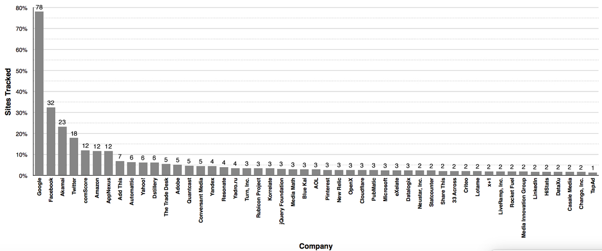
Percentage of sites tracked by top 50 corporations. These 50 corporations were monitoring the greatest percentage of third party data from the Alexa top one million sites studied. (credit: Tim Libert)

A survey of 1 million top websites finds that 88 percent share user data with third parties, according to Tim Libert, a doctoral student at the Annenberg School for Communication at the University of Pennsylvania. The study was published in an open-access paper in the International Journal of Communication.

These websites, listed on Alexa, contact an average of nine external domains, indicating that the activity of a single person visiting a single site may be tracked by multiple entities.

Libert discovered that a handful of U.S. companies receive the vast bulk of user data worldwide, led by Google, which tracked users on nearly 80% of the websites studied. Other top followers on the sites studied include Facebook (32%), Twitter (18%), ComScore (12%), Amazon (12%), and AppNexus (12%).

Elevated security risks

While this monitoring of your behavior doesn’t signal nefarious activity or a security breach, it does increase the risk of one taking place. “If your data is being sent to several companies,” says Libert, “that creates new potential points of failure where your data could be hacked or leaked.”

Using the contents of NSA documents leaked by Edward Snowden, Libert also determined that roughly 20% of websites are potentially vulnerable to known NSA spying techniques. And since a number of large companies are aggregating user data from countless smaller sites, this makes it even easier for government agencies to gather data.

This information may be used to serve you more relevant advertising or to deliver content more quickly, but the ways in which your data is used is not always transparent. And efforts to opt out of that data collection can prove frustrating.

Ostensibly there should be a solution: the browser’s “Do Not Track” (DNT) setting. However Libert’s study found that with the notable exception of Twitter, DNT requests are totally ignored.

“It’s up to regulators to work with companies to comply, because they’re not doing it on their own,” says Libert. “The infrastructure to respect people’s privacy preferences exists, and it works. But unless there are real financial consequences for corporations, they’re just going to ignore DNT. Self-regulation to date has been a big failure.”

This study used Libert’s open-source software platform, webXray, a tool for detecting third-party HTTP requests on large numbers of web pages and matching them to the companies that receive user data. Libert also has made a dataset of the study’s 35 million third-party request records available on his website: timlibert.me.

KurzweilAI’s privacy policy is here.


Abstract of Exposing the Invisible Web: An Analysis of Third-Party HTTP Requests on 1 Million Websites

This article provides a quantitative analysis of privacy-compromising mechanisms on 1 million popular websites. Findings indicate that nearly 9 in 10 websites leak user data to parties of which the user is likely unaware; more than 6 in 10 websites spawn third-party cookies; and more than 8 in 10 websites load Javascript code from external parties onto users’ computers. Sites that leak user data contact an average of nine external domains, indicating that users may be tracked by multiple entities in tandem. By tracing the unintended disclosure of personal browsing histories on the Web, it is revealed that a handful of U.S. companies receive the vast bulk of user data. Finally, roughly 1 in 5 websites are potentially vulnerable to known National Security Agency spying techniques at the time of analysis.