Nanomaterials that mimic nerve impulses (spikes) discovered

Nanomaterials that mimic nerve impulses (credit: Osaka University)

A combination of nanomaterials that can mimic nerve impulses (“spikes”) in the brain have been discovered by researchers at Kyushu Institute of Technology and Osaka University in Japan.

Current “neuromorphic” (brain-like) chips (such as IBM’s neurosynaptic TrueNorth) and circuits (such as those based on the NVIDIA GPGPU, or general purpose graphical processing unit) are devices based on complex circuits that emulate only one part of the brain’s mechanisms: the learning ability of synapses (which connect neurons together).

(Left) Schematic of the SWNT/POM complex network, showing single-wall nanotubes and polyoxometalate (POM) molecules, with gold contacts. (Right) Conductive atomic force microscope image of a molecular neuromorphic network device. (Inset) Molecular structure of polyoxometalate (POM) molecules. (credit: Hirofumi Tanaka et al./Nature Communications)

The researchers have now developed a way to simulate a large-scale spiking neural network. They created a complex SWNT/POM molecular neuromorphic device consisting of a dense and complex network of spiking molecules. The new nanomaterial comprises polyoxometalate (POM) molecules that are absorbed by single-wall carbon nanotubes (SWNTs).

Unlike ordinary organic molecules, POM consists of metal atoms and oxygen atoms that form a three-dimensional framework that can store charges in a single molecule. The new nanomaterial emits spikes and can transmit them via synapses to and from other neurons.

The researchers also demonstrated that this molecular model could be used as a component of reservoir computing devices, which are anticipated as next-generation neural network devices.

Ref: Nature Communications (open access). Source: Osaka University

Discovering new drugs and materials by ‘touching’ molecules in virtual reality

To figure out how to block a bacteria’s attempt to create multi-resistance to antibiotics, a researcher grabs a simulated ligand (binding molecule) — a type of penicillin called benzylpenicillin (red) — and interactively guides that molecule to dock within a larger enzyme molecule (blue-orange) called β-lactamase, which is produced by bacteria in an attempt to disable penicillin (making a patient resistant to a class of antibiotics called β-lactam). (credit: University of Bristol)

University of Bristol researchers, in collaboration with developers at Bristol based start-up Interactive Scientific, Oracle Corporation and a joint team of computer science and chemistry researchers, have designed and tested a new virtual reality (VR) cloud-based system intended to allow researchers to reach out and “touch” molecules as they move — folding them, knotting them, plucking them, and changing their shape to test how the molecules interact. The virtual reality cloud based system, called Nano Simbox, is the proprietary technology of Interactive Scientific, who collaborated with the University of Bristol to do the testing. Using an HTC Vive virtual-reality device, it could lead to creating new drugs and materials and improving the teaching of chemistry.

More broadly, the goal is to accelerate progress in nanoscale molecular engineering areas that include conformational mapping, drug development, synthetic biology, and catalyst design.

Real-time collaboration via the cloud

Two users passing a fullerene (C60) molecule back and forth in real time over a cloud-based network. The researchers are each wearing a VR head-mounted display (HMD) and holding two small wireless controllers that function as atomic “tweezers” to manipulate the real-time molecular dynamic of the C60 molecule. Each user’s position is determined using a real-time optical tracking system composed of synchronized infrared light sources, running locally on a GPU-accelerated computer. (credit: University of Bristol)

The multi-user system, developed by developed by a team led by University of Bristol chemists and computer scientists, uses an “interactive molecular dynamics virtual reality” (iMD VR) app that allows users to visualize and sample (with atomic-level precision) the structures and dynamics of complex molecular structures “on the fly” and to interact with other users in the same virtual environment.

Because each VR client has access to global position data of all other users, any user can see through his/her headset a co-located visual representation of all other users at the same time. So far, the system has uniquely allowed for simultaneously co-locating six users in the same room within the same simulation.

Testing on challenging molecular tasks

The team designed a series of molecular tasks for testing, using traditional mouse, keyboard, and touchscreens compared to virtual reality. The tasks included threading a small molecule through a nanotube, changing the screw-sense of a small organic helix, and tying a small string-like protein into a simple knot, and a variety of dynamic molecular problems, such as binding drugs to its target, protein folding, and chemical reactions. The researchers found that for complex 3D tasks, VR offers a significant advantage over current methods. For example, participants were ten times more likely to succeed in difficult tasks such as molecular knot tying.

Anyone can try out the tasks described in the open-access paper by downloading the software and launching their own cloud-hosted session.


David Glowacki | This video, made by University of Bristol PhD student Helen M. Deeks, shows the actions she took using a wireless set of “atomic tweezers” (using the HTC Vive) to interactively dock a single benzylpenicillin drug molecule into the active site of the β-lactamase enzyme. 


David Glowacki | The video shows the cloud-mounted virtual reality framework, with several different views overlaid to give a sense of how the interaction works. The video outlines the four different parts of the user studies: (1) manipulation of buckminsterfullerene, enabling users to familarize themselves with the interactive controls; (2) threading a methane molecule through a nanotube; (3) changing the screw-sense of a helicene molecule; and (4) tying a trefoil knot in 17-Alanine.

Ref: Science Advances (open-access). Source: University of Bristol.

New material eliminates need for motors or actuators in future robots, other devices

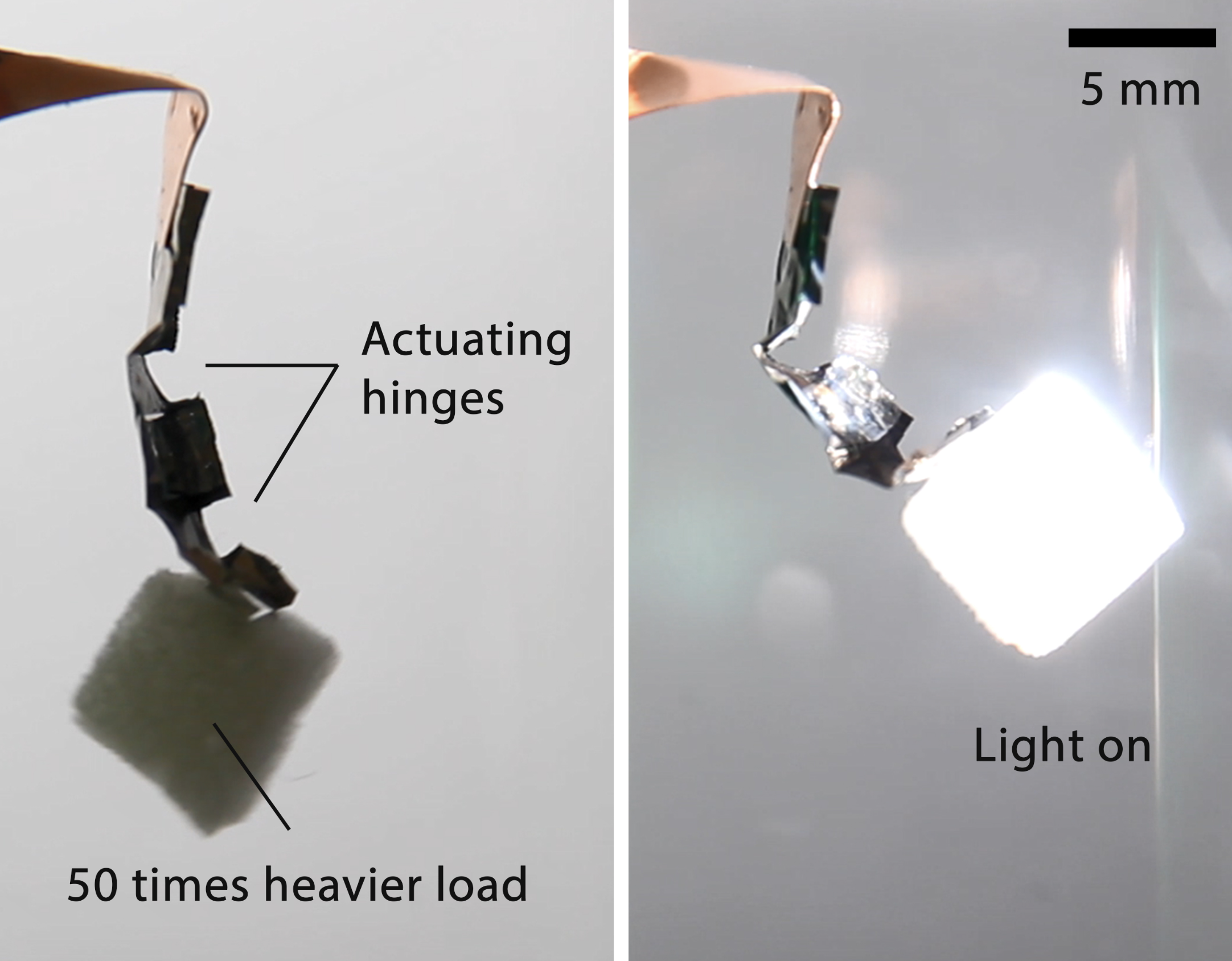
A “mini arm” made up of two hinges of actuating nickel hydroxide-oxyhydroxide material (left) can lift an object 50 times its own weight when triggered (right) by light or electricity. (credit: University of Hong Kong)

University of Hong Kong researchers have invented a radical new lightweight material that could replace traditional bulky, heavy motors or actuators in robots, medical devices, prosthetic muscles, exoskeletons, microrobots, and other types of devices.

The new actuating material — nickel hydroxide-oxyhydroxide — can be instantly triggered and wirelessly powered by low-intensity visible light or electricity at relatively low intensity. It can exert a force of up to 3000 times its own weight — producing stress and speed comparable to mammalian skeletal muscles, according to the researchers.

The material is also responsive to heat and humidity changes, which could allow autonomous machines to harness tiny energy changes in the environment.

The major component is nickel, so the material cost is low, and fabrication uses a simple electrodeposition process, allowing for scaling up and manufacture in industry.

Developing actuating materials was identified as the leading grand challenge in “The grand challenges of Science Robotics” to “deeply root robotics research in science while developing novel robotic platforms that will enable new scientific discoveries.”

Using a light blocker (top) a mini walking bot (bottom) with the “front leg” bent and straightened alternatively can walk towards a light source. (credit: University of Hong Kong)


University of Hong Kong | Future Robots need No Motors

Ref.: Science Robotics. Source: University of Hong Kong.

Ultrasound-powered nanorobots clear bacteria and toxins from blood

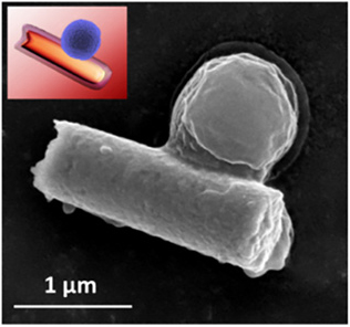
MRSA bacterium captured by a hybrid cell membrane-coated nanorobot (colored scanning electron microscope image and black and white image below) (credit: Esteban-Fernández de Ávila/Science Robotics)

Engineers at the University of California San Diego have developed tiny ultrasound-powered nanorobots that can swim through blood, removing harmful bacteria and the toxins they produce.

These proof-of-concept nanorobots could one day offer a safe and efficient way to detoxify and decontaminate biological threat agents — providing an fast alternative to the multiple, broad-spectrum antibiotics currently used to treat life-threatening pathogens like MRSA bacteria (an antibiotic-resistant staph strain). MRSA is considered a serious worldwide threat to public health.

The MRSA superbug (in yellow) is resistant to antibiotics and can lead to death (credit: National Institute of Allergy and Infectious Diseases)

Antimicrobial resistance (AMR) threatens the effective prevention and treatment of an ever-increasing range of infections caused by bacteria, parasites, viruses and fungi, according to the World Health Organization — an increasingly serious threat to global public health.

Trapping pathogens

The researchers coated gold nanowires with a hybrid of red blood cell membranes and platelets (tiny blood cells that help your body form clots to stop bleeding).*

  • The platelets cloak the nanowires and attract bacterial pathogens, which become bound to the nanorobots.
  • The red blood cells then absorb and neutralize the toxins produced by these bacteria.

Gold nanorobots coated in hybrid platelet/red blood cell membranes (colored scanning electron microscope image). (credit: Esteban-Fernández de Ávila/Science Robotics)

The interior gold nanowire body of the nanorobots responds to ultrasound, causing the nanorobots to swim around rapidly (no chemical fuel required) — mimicking the movement of natural motile cells (such as red blood cells). This mobility helps the nanorobots efficiently mix with their targets (bacteria and toxins) in blood and speed up detoxification.

The coating also protects the nanorobots from a process known as biofouling — when proteins collect onto the surface of foreign objects and prevent them from operating normally.

The nanorobots are just over one micrometer** (1,000 nanometers) long (for comparison, red blood cells have a diameter of 6 to 8 micrometers). The nanorobots can travel up to 35 micrometers per second in blood when powered by ultrasound.

In tests, the researchers used the nanorobots to treat blood samples contaminated with MRSA and their toxins. After five minutes, these blood samples had three times less bacteria and toxins than untreated samples.

Broad-spectrum detoxification

Future work includes tests in mice, making nanorobots out of biodegradable materials instead of gold, and tests of also using the nanorobots for drug delivery.

The ultimate research goal is not to use the nanorobots specifically for treating MRSA infections, but more generally for detoxifying biological fluids — “an important step toward the creation of a broad-spectrum detoxification robotic platform,” as the researchers note in a paper.

* The researchers created the nanorobots in three steps:

1. They created the hybrid coating by first separating entire membranes from platelets and red blood cells.

2. They applied ultrasound (high-frequency sound waves) to fuse the membranes together. (Since the membranes were taken from actual cells, they contain all their original-cell surface protein functions, including the ability of platelets to attract bacteria.)

3. They coated these hybrid membranes onto gold nanowires.

** A micrometer is one millionth of a meter, or one thousandth of a millimeter.

This work was supported by the Defense Threat Reduction Agency Joint Science and Technology Office for Chemical and Biological Defense.

Reference: Science Robotics. Source: UC San Diego.

First 3D-printed human corneas

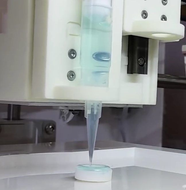
3D-printing a human cornea (credit: Newcastle University)

Scientists at Newcastle University have created a proof-of-concept process to achieve the first 3D-printed human corneas (the cornea, the outermost layer of the human eye, has an important role in focusing vision).*

Stem cells (human corneal stromal cells) from a healthy donor’s cornea were mixed together with alginate and collagen** to create a “bio-ink” solution. Using a simple low-cost 3D bio-printer, the bio-ink was successfully extruded in concentric circles to form the shape of a human cornea in less than 10 minutes.

They also demonstrated that they could build a cornea to match a patient’s unique specifications, based on a scan of the patient’s eye.

The technique could be used in the future to ensure an unlimited supply of corneas, but it will be several years of testing before they could be used in transplants, according to the scientists.

* There is a significant shortage of corneas available to transplant, with 10 million people worldwide requiring surgery to prevent corneal blindness as a result of diseases such as trachoma, an infectious eye disorder. In addition, almost 5 million people suffer total blindness due to corneal scarring caused by burns, lacerations, abrasion or disease.

* This mixture keeps the stem cells alive, and it’s stiff enough to hold its shape but soft enough to be squeezed out of the nozzle of a 3D printer.

Reference: Experimental Eye Research. Source: Newcastle University


High-quality carbon nanotubes made from carbon dioxide in the air break the manufacturing cost barrier

Carbon dioxide converted to small-diameter carbon nanotubes grown on a stainless steel surface. (credit: Pint Lab/Vanderbilt University)

Vanderbilt University researchers have discovered a technique to cost-effectively convert carbon dioxide from the air into a type of carbon nanotubes that they say is “more valuable than any other material ever made.”

Carbon nanotubes are super-materials that can be stronger than steel and more conductive than copper. So despite much research, why aren’t they used in applications ranging from batteries to tires?

Answer: The high manufacturing costs and extremely expensive price, according to the researchers.*

The price ranges from $100–200 per kilogram for the “economy class” carbon nanotubes with larger diameters and poorer properties, up to $100,000 per kilogram and above for the “first class” carbon nanotubes — ones with a single wall, the smallest diameters**, and the most amazing properties, Cary Pint, PhD, an assistant professor in the Mechanical Engineering department at Vanderbilt University, explained to KurzweilAI.

A new process for making cost-effective carbon nanotubes

The researchers have demonstrated a new process for creating carbon-nanotube-based material, using carbon dioxide as a feedstock input source.

  • They achieved the smallest-diameter and most valuable CNTs ever reported in the literature for this approach.
  • They used sustainable electrochemical synthesis.***
  • A spinoff, SkyNano LLC, is now doing this with far less cost and energy input than conventional methods for making these materials. “That means as market prices start to change, our technology will survive and the more expensive technologies will get shaken out of the market,” said Pint. “We’re aggressively working toward scaling this process up in a big way.”
  • There are implications for reducing carbon dioxide in the atmosphere.****

“One of the most exciting things about what we’ve done is use electrochemistry to pull apart carbon dioxide into elemental constituents of carbon and oxygen and stitch together, with nanometer precision, those carbon atoms into new forms of matter,” said Pint. “That opens the door to being able to generate really valuable products with carbon nanotubes.” These materials, which Pint calls “black gold,” could steer the conversation from the negative impact of emissions to how we can use them in future technology.

“These could revolutionize the world,” he said.

Reference: ACS Appl. Mater. Interfaces May 1, 2018. Source: Vanderbilt University

* This BCC Research market report has a detailed discussion on carbon nanotube costsGlobal Markets and Technologies for Carbon Nanotubes. Also see Energy requirements,an open-access supplement to the ACS paper.

** “Small-diameter” in this study refers to about 10 nanometers or less. Small-diameter carbon nanotubes include few-walled (about 310 walls), double-walled, and single walled carbon nanotubes. These all have higher economic value because of their enhanced physical properties, broader appeal toward applications, and greater difficulty in synthesis compared to their larger-diameter counterparts. “Larger diameter” carbon nanotubes refer to those with outer diameter generally less than 50 nanometers, since after reaching this diameter, these materials lose the value that the properties in small diameter carbon nanotubes enable for applications.

*** The researchers used mechanisms for controlling electrochemical synthesis of CNTs from the capture and conversion of ambient CO2 in molten salts. Iron catalyst layers are deposited at different thicknesses onto stainless steel to produce cathodes, and atomic layer deposition of Al2O3 (aluminum oxide) is performed on nickel to produce a corrosion-resistant anode. The research team showed that a process called “Ostwald ripening” — where the nanoparticles that grow the carbon nanotubes change in size to larger diameters — is a key contender against producing the infinitely more useful size. The team showed they could partially overcome this by tuning electrochemical parameters to minimize these pesky large nanoparticles.

**** “According to the EPA, the United States alone emits more than 6,000 million metric tons of carbon dioxide into the atmosphere every year.  Besides being implicated as a contributor to global climate change, these emissions are currently wasted resources that could otherwise be used productively to make useful materials. At SkyNano, we focus on the electrochemical conversion of carbon dioxide into all carbon-based nanomaterials which can be used for a variety of applications. Our technology overcomes cost limitations associated with traditional carbon nanomaterial production and utilizes carbon dioxide as the only direct chemical feedstock.” — SkyNano Technologies

New sensors monitor brain activity and blood flow deeper in the brain with high sensitivity and high speed

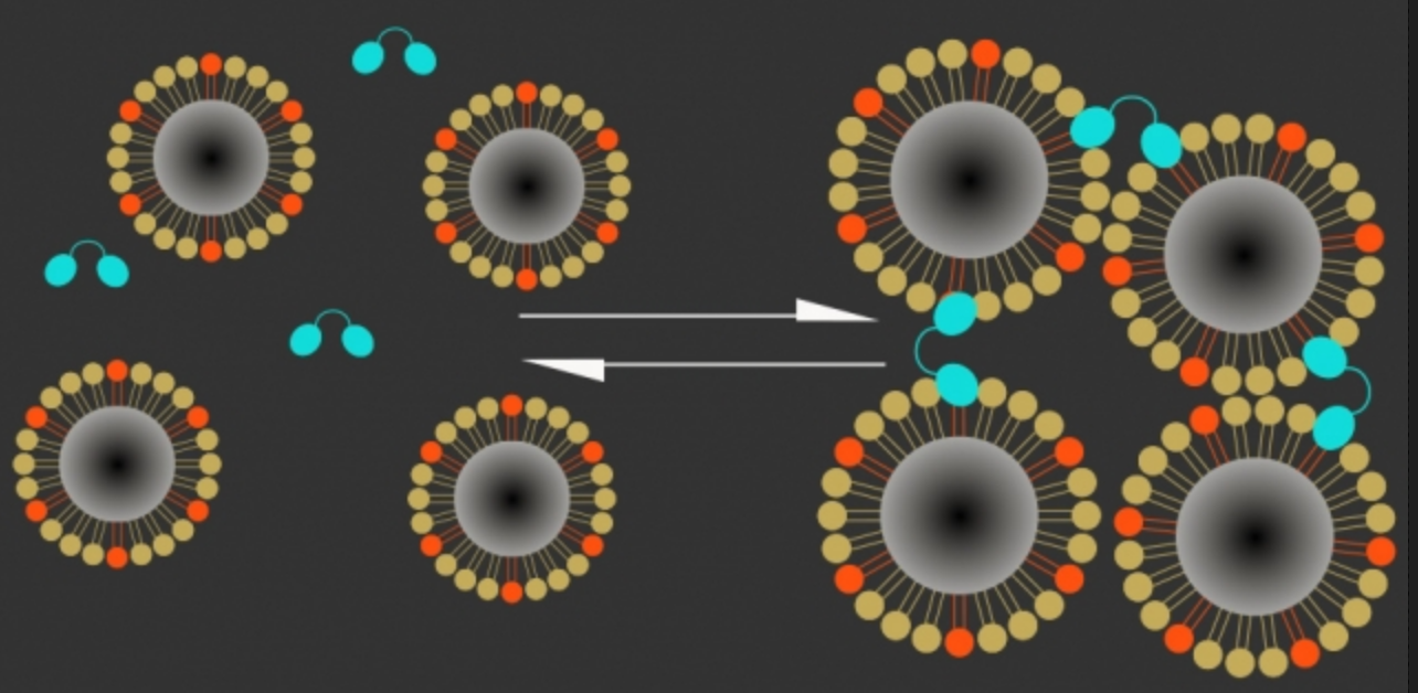
Magnetic calcium-responsive nanoparticles (dark centers are magnetic cores) respond within seconds to calcium ion changes by clustering (Ca+ ions, right) or expanding (Ca- ions, left), creating a magnetic contrast change that can be detected with MRI, indicating brain activation. (High levels of calcium outside the neurons correlate with low neuron activity; when calcium concentrations drop, it means neurons in that area are firing electrical impulses.) Blue: C2AB “molecular glue” (credit: The researchers)

Calcium-based MRI sensor enables deep brain imaging

MIT neuroscientists have developed a new magnetic resonance imaging (MRI) sensor that allows them to monitor neural activity deep within the brain by tracking calcium ions.

Calcium ions are directly linked to neuronal firing at high resolution — unlike the changes in blood flow detected by functional MRI (fMRI), which provide only an indirect indication of neural activity. The new sensor can also monitor large areas, compared to fluorescent molecules, used to label calcium in the brain and image it with traditional microscopy, which is limited to small areas of the brain.

A calcium-based MRI sensor could allow researchers to link specific brain functions directly to specific neuron activity, and to determine how distant brain regions communicate with each other during particular tasks. The research is described in a paper in the April 30 issue of Nature Nanotechnology. Source: MIT

New technique for measuring blood flow in the brain uses laser light shined into the head (“sample arm” path) through the skull. The return signal is boosted by a reference light beam and returned to a detector camera chip. (credit: Srinivasan lab, UC Davis)

Measuring deep-tissue blood flow at high speed

Biomedical engineers at the University of California, Davis, have developed a more-effective, lower-cost technique for measuring deep tissue blood flow in the brain at high speed. It could be especially useful for patients with stroke or traumatic brain injury.

The technique, called “interferometric diffusing wave spectroscopy” (iDWS), replaces about 20 photon-counting detectors in diffusing wave spectroscopy (DWS) devices (which cost a few thousand dollars each) with a single low-cost CMOS-based digital-camera chip.

The NIH-funded work is described in an open-access paper published April 26 in the journal Optica. Source: UC Davis


Metalens with artificial muscle simulates (and goes way beyond) human-eye and camera optical functions

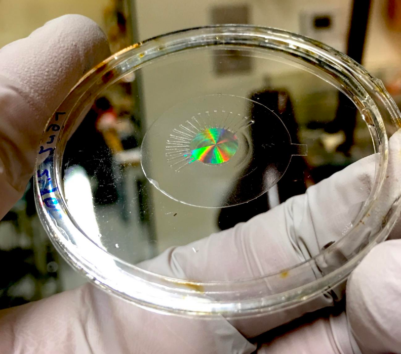
A silicon-based metalens just 30 micrometers thick is mounted on a transparent, stretchy polymer film. The colored iridescence is produced by the large number of nanostructures within the metalens. (credit:Harvard SEAS)

Researchers at the Harvard John A. Paulson School of Engineering and Applied Sciences (SEAS) have developed a breakthrough electronically controlled artificial eye. The thin, flat, adaptive silicon nanostructure (“metalens”) can simultaneously control focus, astigmatism, and image shift (three of the major contributors to blurry images) in real time, which the human eye (and eyeglasses) cannot do.

The 30-micrometers-thick metalens makes changes laterally to achieve optical zoom, autofocus, and image stabilization — making it possible to replace bulky lens systems in future optical systems used in eyeglasses, cameras, cell phones, and augmented and virtual reality devices.

The research is described in an open-access paper in Science Advances. In another paper recently published in Optics Express, the researchers demonstrated the design and fabrication of metalenses up to centimeters or more in diameter.* That makes it possible to unify two industries: semiconductor manufacturing and lens-making. So the same technology used to make computer chips will be used to make metasurface-based optical components, such as lenses.

The adaptive metalens (right) focuses light rays onto an image sensor (left), such as one in a camera. An electrical signal controls the shape of the metalens to produce the desired optical wavefront patterns (shown in red), resulting in improved images. In the future, adaptive metalenses will be built into imaging systems, such as cell phone cameras and microscopes, enabling flat, compact autofocus as well as the capability for simultaneously correcting optical aberrations and performing optical image stabilization, all in a single plane of control. (credit: Second Bay Studios/Harvard SEAS)

Simulating the human eye’s lens and ciliary muscles

In the human eye, the lens is surrounded by ciliary muscle, which stretches or compresses the lens, changing its shape to adjust its focal length. To achieve that function, the researchers adhered a metalens to a thin, transparent dielectric elastomer actuator (“artificial muscle”). The researchers chose a dielectic elastomer with low loss — meaning light travels through the material with little scattering — to attach to the lens.

(Top) Schematic of metasurface and dielectric elastomer actuators (“artificial muscles”), showing how the new artificial muscles change focus, similar to how the ciliary muscle in the eye work. An applied voltage supplies transparent, stretchable electrode layers (gray), made up of single-wall carbon-nanotube nanopillars, with electrical charges (acting as a capacitor). The resulting electrostatic attraction compresses (red arrows) the dielectric elastomer actuators (artificial muscles) in the thickness direction and expands (black arrows) the elastomers in the lateral direction. The silicon metasurface (in the center), applied by photolithography, can simultaneously focus, control aberrations caused by astigmatisms, and perform image shift. (Bottom) Photo of actual device. (credit: Alan She et al./Sci. Adv.)

Next, the researchers aim to further improve the functionality of the lens and decrease the voltage required to control it.

The research was performed at the Harvard John A. Paulson School of Engineering and Applied Sciences, supported in part by the Air Force Office of Scientific Research and by the National Science Foundation. This work was performed in part at the Center for Nanoscale Systems (CNS), which is supported by the National Science Foundation. The Harvard Office of Technology Development is exploring commercialization opportunities.

* To build the artificial eye with a larger (more functional) metalens, the researchers had to develop a new algorithm to shrink the file size to make it compatible with the technology currently used to fabricate integrated circuits.

** “All optical systems with multiple components — from cameras to microscopes and telescopes — have slight misalignments or mechanical stresses on their components, depending on the way they were built and their current environment, that will always cause small amounts of astigmatism and other aberrations, which could be corrected by an adaptive optical element,” said Alan She, a graduate student at SEAS and first author of the paper. “Because the adaptive metalens is flat, you can correct those aberrations and integrate different optical capabilities onto a single plane of control. Our results demonstrate the feasibility of embedded autofocus, optical zoom, image stabilization, and adaptive optics, which are expected to become essential for future chip-scale image sensors and  Furthermore, the device’s flat construction and inherently lateral actuation without the need for motorized parts allow for highly stackable systems such as those found in stretchable electronic eye camera sensors, providing possibilities for new kinds of imaging systems.”


Abstract of Adaptive metalenses with simultaneous electrical control of focal length, astigmatism, and shift

Focal adjustment and zooming are universal features of cameras and advanced optical systems. Such tuning is usually performed longitudinally along the optical axis by mechanical or electrical control of focal length. However, the recent advent of ultrathin planar lenses based on metasurfaces (metalenses), which opens the door to future drastic miniaturization of mobile devices such as cell phones and wearable displays, mandates fundamentally different forms of tuning based on lateral motion rather than longitudinal motion. Theory shows that the strain field of a metalens substrate can be directly mapped into the outgoing optical wavefront to achieve large diffraction-limited focal length tuning and control of aberrations. We demonstrate electrically tunable large-area metalenses controlled by artificial muscles capable of simultaneously performing focal length tuning (>100%) as well as on-the-fly astigmatism and image shift corrections, which until now were only possible in electron optics. The device thickness is only 30 μm. Our results demonstrate the possibility of future optical microscopes that fully operate electronically, as well as compact optical systems that use the principles of adaptive optics to correct many orders of aberrations simultaneously.


Abstract of Large area metalenses: design, characterization, and mass manufacturing

Optical components, such as lenses, have traditionally been made in the bulk form by shaping glass or other transparent materials. Recent advances in metasurfaces provide a new basis for recasting optical components into thin, planar elements, having similar or better performance using arrays of subwavelength-spaced optical phase-shifters. The technology required to mass produce them dates back to the mid-1990s, when the feature sizes of semiconductor manufacturing became considerably denser than the wavelength of light, advancing in stride with Moore’s law. This provides the possibility of unifying two industries: semiconductor manufacturing and lens-making, whereby the same technology used to make computer chips is used to make optical components, such as lenses, based on metasurfaces. Using a scalable metasurface layout compression algorithm that exponentially reduces design file sizes (by 3 orders of magnitude for a centimeter diameter lens) and stepper photolithography, we show the design and fabrication of metasurface lenses (metalenses) with extremely large areas, up to centimeters in diameter and beyond. Using a single two-centimeter diameter near-infrared metalens less than a micron thick fabricated in this way, we experimentally implement the ideal thin lens equation, while demonstrating high-quality imaging and diffraction-limited focusing.

Metalens with artificial muscle simulates (and goes way beyond) human-eye and camera optical functions

A silicon-based metalens just 30 micrometers thick is mounted on a transparent, stretchy polymer film. The colored iridescence is produced by the large number of nanostructures within the metalens. (credit:Harvard SEAS)

Researchers at the Harvard John A. Paulson School of Engineering and Applied Sciences (SEAS) have developed a breakthrough electronically controlled artificial eye. The thin, flat, adaptive silicon nanostructure (“metalens”) can simultaneously control focus, astigmatism, and image shift (three of the major contributors to blurry images) in real time, which the human eye (and eyeglasses) cannot do.

The 30-micrometers-thick metalens makes changes laterally to achieve optical zoom, autofocus, and image stabilization — making it possible to replace bulky lens systems in future optical systems used in eyeglasses, cameras, cell phones, and augmented and virtual reality devices.

The research is described in an open-access paper in Science Advances. In another paper recently published in Optics Express, the researchers demonstrated the design and fabrication of metalenses up to centimeters or more in diameter.* That makes it possible to unify two industries: semiconductor manufacturing and lens-making. So the same technology used to make computer chips will be used to make metasurface-based optical components, such as lenses.

The adaptive metalens (right) focuses light rays onto an image sensor (left), such as one in a camera. An electrical signal controls the shape of the metalens to produce the desired optical wavefront patterns (shown in red), resulting in improved images. In the future, adaptive metalenses will be built into imaging systems, such as cell phone cameras and microscopes, enabling flat, compact autofocus as well as the capability for simultaneously correcting optical aberrations and performing optical image stabilization, all in a single plane of control. (credit: Second Bay Studios/Harvard SEAS)

Simulating the human eye’s lens and ciliary muscles

In the human eye, the lens is surrounded by ciliary muscle, which stretches or compresses the lens, changing its shape to adjust its focal length. To achieve that function, the researchers adhered a metalens to a thin, transparent dielectric elastomer actuator (“artificial muscle”). The researchers chose a dielectic elastomer with low loss — meaning light travels through the material with little scattering — to attach to the lens.

(Top) Schematic of metasurface and dielectric elastomer actuators (“artificial muscles”), showing how the new artificial muscles change focus, similar to how the ciliary muscle in the eye work. An applied voltage supplies transparent, stretchable electrode layers (gray), made up of single-wall carbon-nanotube nanopillars, with electrical charges (acting as a capacitor). The resulting electrostatic attraction compresses (red arrows) the dielectric elastomer actuators (artificial muscles) in the thickness direction and expands (black arrows) the elastomers in the lateral direction. The silicon metasurface (in the center), applied by photolithography, can simultaneously focus, control aberrations caused by astigmatisms, and perform image shift. (Bottom) actual device. (credit: She et al./Sci. Adv.)

Next, the researchers aim to further improve the functionality of the lens and decrease the voltage required to control it.

The research was performed at the Harvard John A. Paulson School of Engineering and Applied Sciences, supported in part by the Air Force Office of Scientific Research and by the National Science Foundation. This work was performed in part at the Center for Nanoscale Systems (CNS), which is supported by the National Science Foundation. The Harvard Office of Technology Development is exploring commercialization opportunities.

* To build the artificial eye with a larger (more functional) metalens, the researchers had to develop a new algorithm to shrink the file size to make it compatible with the technology currently used to fabricate integrated circuits.

** “All optical systems with multiple components — from cameras to microscopes and telescopes — have slight misalignments or mechanical stresses on their components, depending on the way they were built and their current environment, that will always cause small amounts of astigmatism and other aberrations, which could be corrected by an adaptive optical element,” said Alan She, a graduate student at SEAS and first author of the paper. “Because the adaptive metalens is flat, you can correct those aberrations and integrate different optical capabilities onto a single plane of control. Our results demonstrate the feasibility of embedded autofocus, optical zoom, image stabilization, and adaptive optics, which are expected to become essential for future chip-scale image sensors and  Furthermore, the device’s flat construction and inherently lateral actuation without the need for motorized parts allow for highly stackable systems such as those found in stretchable electronic eye camera sensors, providing possibilities for new kinds of imaging systems.”


Abstract of Adaptive metalenses with simultaneous electrical control of focal length, astigmatism, and shift

Focal adjustment and zooming are universal features of cameras and advanced optical systems. Such tuning is usually performed longitudinally along the optical axis by mechanical or electrical control of focal length. However, the recent advent of ultrathin planar lenses based on metasurfaces (metalenses), which opens the door to future drastic miniaturization of mobile devices such as cell phones and wearable displays, mandates fundamentally different forms of tuning based on lateral motion rather than longitudinal motion. Theory shows that the strain field of a metalens substrate can be directly mapped into the outgoing optical wavefront to achieve large diffraction-limited focal length tuning and control of aberrations. We demonstrate electrically tunable large-area metalenses controlled by artificial muscles capable of simultaneously performing focal length tuning (>100%) as well as on-the-fly astigmatism and image shift corrections, which until now were only possible in electron optics. The device thickness is only 30 μm. Our results demonstrate the possibility of future optical microscopes that fully operate electronically, as well as compact optical systems that use the principles of adaptive optics to correct many orders of aberrations simultaneously.


Abstract of Large area metalenses: design, characterization, and mass manufacturing

Optical components, such as lenses, have traditionally been made in the bulk form by shaping glass or other transparent materials. Recent advances in metasurfaces provide a new basis for recasting optical components into thin, planar elements, having similar or better performance using arrays of subwavelength-spaced optical phase-shifters. The technology required to mass produce them dates back to the mid-1990s, when the feature sizes of semiconductor manufacturing became considerably denser than the wavelength of light, advancing in stride with Moore’s law. This provides the possibility of unifying two industries: semiconductor manufacturing and lens-making, whereby the same technology used to make computer chips is used to make optical components, such as lenses, based on metasurfaces. Using a scalable metasurface layout compression algorithm that exponentially reduces design file sizes (by 3 orders of magnitude for a centimeter diameter lens) and stepper photolithography, we show the design and fabrication of metasurface lenses (metalenses) with extremely large areas, up to centimeters in diameter and beyond. Using a single two-centimeter diameter near-infrared metalens less than a micron thick fabricated in this way, we experimentally implement the ideal thin lens equation, while demonstrating high-quality imaging and diffraction-limited focusing.

Ultra-thin ‘atomistor’ synapse-like memory storage device paves way for faster, smaller, smarter computer chips

Illustration of single-atom-layer “atomristors” — the thinnest-ever memory-storage device (credit: Cockrell School of Engineering, The University of Texas at Austin)

A team of electrical engineers at The University of Texas at Austin and scientists at Peking University has developed a one-atom-thick 2D “atomristor” memory storage device that may lead to faster, smaller, smarter computer chips.

The atomristor (atomic memristor) improves upon memristor (memory resistor) memory storage technology by using atomically thin nanomaterials (atomic sheets). (Combining memory and logic functions, similar to the synapses of biological brains, memristors “remember” their previous state after being turned off.)

Schematic of atomristor memory sandwich based on molybdenum sulfide (MoS2) in a form of a single-layer atomic sheet grown on gold foil. (Blue: Mo; yellow: S) (credit: Ruijing Ge et al./Nano Letters)

Memory storage and transistors have, to date, been separate components on a microchip. Atomristors combine both functions on a single, more-efficient device. They use metallic atomic sheets (such as graphene or gold) as electrodes and semiconducting atomic sheets (such as molybdenum sulfide) as the active layer. The entire memory cell is a two-layer sandwich only ~1.5 nanometers thick.

“The sheer density of memory storage that can be made possible by layering these synthetic atomic sheets onto each other, coupled with integrated transistor design, means we can potentially make computers that learn and remember the same way our brains do,” said Deji Akinwande, associate professor in the Cockrell School of Engineering’s Department of Electrical and Computer Engineering.

“This discovery has real commercialization value, as it won’t disrupt existing technologies,” Akinwande said. “Rather, it has been designed to complement and integrate with the silicon chips already in use in modern tech devices.”

The research is described in an open-access paper in the January American Chemical Society journal Nano Letters.

Longer battery life in cell phones

For nonvolatile operation (preserving data after power is turned off), the new design also “offers a substantial advantage over conventional flash memory, which occupies far larger space. In addition, the thinness allows for faster and more efficient electric current flow,” the researchers note in the paper.

The research team also discovered another unique application for the atomristor technology: Atomristors are the smallest radio-frequency (RF) memory switches to be demonstrated, with no DC battery consumption, which could ultimately lead to longer battery life for cell phones and other battery-powered devices.*

Funding for the UT Austin team’s work was provided by the National Science Foundation and the Presidential Early Career Award for Scientists and Engineers, awarded to Akinwande in 2015.

* “Contemporary switches are realized with transistor or microelectromechanical devices, both of which are volatile, with the latter also requiring large switching voltages [which are not ideal] for mobile technologies,” the researchers note in the paper. Atomristors instead allow for nonvolatile low-power radio-frequency (RF) switches with “low voltage operation, small form-factor, fast switching speed, and low-temperature integration compatible with silicon or flexible substrates.”


Abstract of Atomristor: Nonvolatile Resistance Switching in Atomic Sheets of Transition Metal Dichalcogenides

Recently, two-dimensional (2D) atomic sheets have inspired new ideas in nanoscience including topologically protected charge transport,1,2 spatially separated excitons,3 and strongly anisotropic heat transport.4 Here, we report the intriguing observation of stable nonvolatile resistance switching (NVRS) in single-layer atomic sheets sandwiched between metal electrodes. NVRS is observed in the prototypical semiconducting (MX2, M = Mo, W; and X = S, Se) transitional metal dichalcogenides (TMDs),5 which alludes to the universality of this phenomenon in TMD monolayers and offers forming-free switching. This observation of NVRS phenomenon, widely attributed to ionic diffusion, filament, and interfacial redox in bulk oxides and electrolytes,6−9 inspires new studies on defects, ion transport, and energetics at the sharp interfaces between atomically thin sheets and conducting electrodes. Our findings overturn the contemporary thinking that nonvolatile switching is not scalable to subnanometre owing to leakage currents.10 Emerging device concepts in nonvolatile flexible memory fabrics, and brain-inspired (neuromorphic) computing could benefit substantially from the wide 2D materials design space. A new major application, zero-static power radio frequency (RF) switching, is demonstrated with a monolayer switch operating to 50 GHz.