First transistors made entirely of nanocrystal ‘inks’ in simplified process

Because this process works at relatively low temperatures, many transistors can be made on a flexible backing at once. (credit: University of Pennsylvania)

University of Pennsylvania engineers have developed a simplified new approach for making transistors by sequentially depositing their components in the form of liquid nanocrystal “inks.” The new process open the door for transistors and other electronic components to be built into flexible or wearable applications. It also avoids the highly complex current process for creating transistors, which requires high-temperature, high-vacuum equipment. Also, the new lower-temperature process is compatible with a wide array of materials and can be applied to larger areas.

Transistors patterned on plastic backing

The researchers’ nanocrystal-based field effect transistors were patterned onto flexible plastic backings using spin coating, but could eventually be constructed by additive manufacturing systems, like 3D printers.

Published in the journal Science,  the study was lead by Cherie Kagan, the Stephen J. Angello Professor in the School of Engineering and Applied Science, and Ji-Hyuk Choi, then a member of her lab, now a senior researcher at the Korea Institute of Geoscience and Mineral Resources. Researchers at Korea University Korea’s Yonsei University were also involved.

Kagan’s group developed four nanocrystal inks that comprise the transistor, then deposited them on a flexible backing. (credit: University of Pennsylvania)

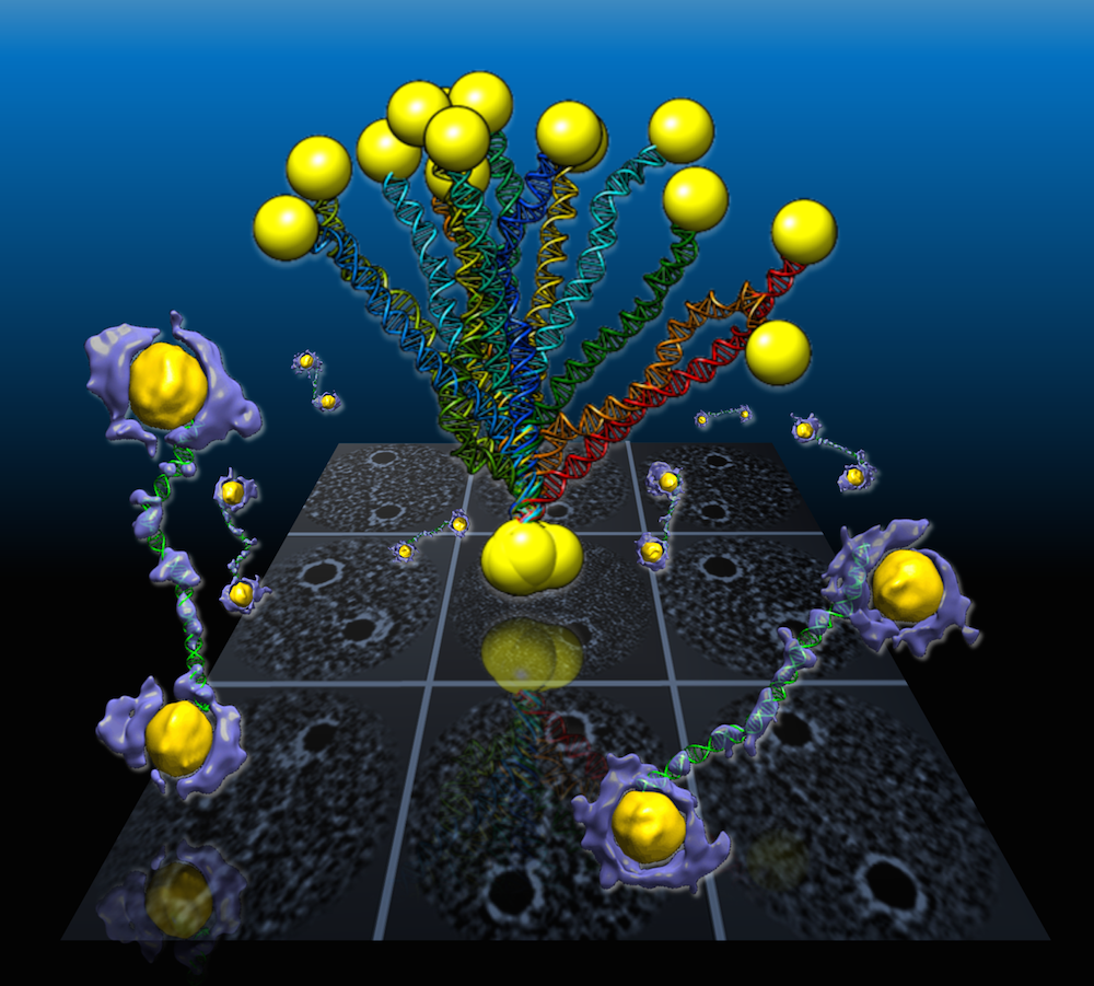
The researchers began by dispersing a specific type of nanocrystals in a liquid, creating nanocrystal inks. They developed a library of four of these inks: a conductor (silver), an insulator (aluminum oxide), a semiconductor (cadmium selenide), and a conductor combined with a dopant (a mixture of silver and indium). (“Doping” the semiconductor layer of a transistor with impurities controls whether the device creates a positive or negative charge.)

“These materials are colloids just like the ink in your inkjet printer,” Kagan said, “but you can get all the characteristics that you want and expect from the analogous bulk materials, such as whether they’re conductors, semiconductors or insulators.” Although the electrical properties of several of these nanocrystal inks had been independently verified, they had never been combined into full devices. “Our question was whether you could lay them down on a surface in such a way that they work together to form functional transistors.”

Laying down patterns in layers

Such a process entails layering or mixing them in precise patterns.

First, the conductive silver nanocrystal ink was deposited from liquid on a flexible plastic surface that was treated with a photolithographic mask, then rapidly spun to draw it out in an even layer. The mask was then removed to leave the silver ink in the shape of the transistor’s gate electrode.

The researchers followed that layer by spin-coating a layer of the aluminum oxide nanocrystal-based insulator, then a layer of the cadmium selenide nanocrystal-based semiconductor and finally another masked layer for the indium/silver mixture, which forms the transistor’s source and drain electrodes. Upon heating at relatively low temperatures, the indium dopant diffused from those electrodes into the semiconductor component.

“The trick with working with solution-based materials is making sure that, when you add the second layer, it doesn’t wash off the first, and so on,” Kagan said. “We had to treat the surfaces of the nanocrystals, both when they’re first in solution and after they’re deposited, to make sure they have the right electrical properties and that they stick together in the configuration we want.”

Because this entirely ink-based fabrication process works at lower temperatures than existing vacuum-based methods, the researchers were able to make several transistors on the same flexible plastic backing at the same time.

The inks’ specialized surface chemistry allowed them to stay in configuration without losing their electrical properties. (credit: University of Pennsylvania)

“Making transistors over larger areas and at lower temperatures have been goals for an emerging class of technologies, when people think of the Internet of things, large area flexible electronics and wearable devices,” Kagan said. “We haven’t developed all of the necessary aspects so they could be printed yet, but because these materials are all solution-based, it demonstrates the promise of this materials class and sets the stage for additive manufacturing.”

Because this entirely ink-based fabrication process works at lower temperatures than existing vacuum-based methods, the researchers were able to make several transistors on the same flexible plastic backing at the same time.

3D-printing transistors for wearables

“This is the first work,” Choi said, “showing that all the components, the metallic, insulating, and semiconducting layers of the transistors, and even the doping of the semiconductor, could be made from nanocrystals.”

“Making transistors over larger areas and at lower temperatures have been goals for an emerging class of technologies, when people think of the Internet of things, large area flexible electronics and wearable devices,” Kagan said. “We haven’t developed all of the necessary aspects so they could be printed yet, but because these materials are all solution-based, it demonstrates the promise of this materials class and sets the stage for additive manufacturing.”

The research was supported by the National Science Foundation, the U.S. Department of Energy, the Office of Naval Research, and the Korea Institute of Geoscience and Mineral Resources funded by the Ministry of Science, ICT, and Future Planning of Korea.


Abstract of Exploiting the colloidal nanocrystal library to construct electronic devices

Synthetic methods produce libraries of colloidal nanocrystals with tunable physical properties by tailoring the nanocrystal size, shape, and composition. Here, we exploit colloidal nanocrystal diversity and design the materials, interfaces, and processes to construct all-nanocrystal electronic devices using solution-based processes. Metallic silver and semiconducting cadmium selenide nanocrystals are deposited to form high-conductivity and high-mobility thin-film electrodes and channel layers of field-effect transistors. Insulating aluminum oxide nanocrystals are assembled layer by layer with polyelectrolytes to form high–dielectric constant gate insulator layers for low-voltage device operation. Metallic indium nanocrystals are codispersed with silver nanocrystals to integrate an indium supply in the deposited electrodes that serves to passivate and dope the cadmium selenide nanocrystal channel layer. We fabricate all-nanocrystal field-effect transistors on flexible plastics with electron mobilities of 21.7 square centimeters per volt-second.

Best textile manufacturing methods for creating human tissues with stem cells

All four textile manufacturing processes and corresponding scaffold (structure) types studied exhibited the presence of lipid vacuoles (small red spheres, right column, indicating stem cells undergoing random differentiation), compared to control (left). Electrospun scaffolds (row a) exhibited only a monolayer of lipid vacuoles in a single focal plane, while meltblown, spunbond, and carded scaffolds (rows b, c, d) exhibited vacuoles in multiple planes throughout the fabric thickness. Scale bars: 100 μm (credit: S. A. Tuin et al./Biomedical Materials)

Elizabeth Loboa, dean of the Missouri University College of Engineering, and her team have tested new tissue- engineering methods (based on textile manufacturing) to find ones that are most cost-effective and can be produced in larger quantities.

Tissue engineering is a process that uses novel biomaterials seeded with stem cells to grow and replace missing tissues. When certain types of materials are used, the “scaffolds” that are created to hold stem cells eventually degrade, leaving natural tissue in its place. The new tissues could help patients suffering from wounds caused by diabetes and circulation disorders, patients in need of cartilage or bone repair, and women who have had mastectomies by replacing their breast tissue. The challenge is creating enough of the material on a scale that clinicians need to treat patients.

Comparing textile manufacturing techniques

Electrospinning experiment: nanofibers are collected into an ethanol bath and removed at predefined time intervals (credit: J. M. Coburn et al./The Johns Hopkins University/PNAS)

In typical tissue engineering approaches that use fibers as scaffolds, non-woven materials are often bonded together using an electrostatic field. This process, called electrospinning (see Nanoscale scaffolds and stem cells show promise in cartilage repair and Improved artificial blood vessels), creates the scaffolds needed to attach to stem cells.

However, large-scale production with electrospinning is not cost-effective. “Electrospinning produces weak fibers, scaffolds that are not consistent, and pores that are too small,” Loboa said. “The goal of ‘scaling up’ is to produce hundreds of meters of material that look the same, have the same properties, and can be used in clinical settings. So we investigated the processes that create textiles, such as clothing and window furnishings like drapery, to scale up the manufacturing process.”

The group published two papers using three industry-standard, high-throughput manufacturing techniques — meltblowing, spunbonding, and carding — to determine if they would create the materials needed to mimic native tissue.

Meltblowing is a technique during which nonwoven materials are created using a molten polymer to create continuous fibers. Spunbond materials are made much the same way but the fibers are drawn into a web while in a solid state instead of a molten one. Carding involves the separation of fibers through the use of rollers, forming the web needed to hold stem cells in place.

Schematic of gilled fiber multifilament spinning and carded scaffold fabrication (credit: Stephen A. Tuin et al./Acta Biomaterialia)

Cost-effective methods

Loboa and her colleagues tested these techniques to create polylactic acid (PLA) scaffolds (a Food and Drug Administration-approved material used as collagen fillers), seeded with human stem cells. They then spent three weeks studying whether the stem cells remained healthy and if they began to differentiate into fat and bone pathways, which is the goal of using stem cells in a clinical setting when new bone and/or new fat tissue is needed at a defect site. Results showed that the three textile manufacturing methods proved as viable if not more so than electrospinning.

“These alternative methods are more cost-effective than electrospinning,” Loboa said. “A small sample of electrospun material could cost between $2 to $5. The cost for the three manufacturing methods is between $.30 to $3.00; these methods proved to be effective and efficient. Next steps include testing how the different scaffolds created in the three methods perform once implanted in animals.”

Researchers at North Carolina State University and the University of North Carolina at Chapel Hill were also involved in the two studies, which were published in Biomedical Materials (open access) and Acta Biomaterialia. The National Science Foundation, the National Institutes of Health, and the Nonwovens Institute provided funding for the studies.


Abstract of Creating tissues from textiles: scalable nonwoven manufacturing techniques for fabrication of tissue engineering scaffolds

Electrospun nonwovens have been used extensively for tissue engineering applications due to their inherent similarities with respect to fibre size and morphology to that of native extracellular matrix (ECM). However, fabrication of large scaffold constructs is time consuming, may require harsh organic solvents, and often results in mechanical properties inferior to the tissue being treated. In order to translate nonwoven based tissue engineering scaffold strategies to clinical use, a high throughput, repeatable, scalable, and economic manufacturing process is needed. We suggest that nonwoven industry standard high throughput manufacturing techniques (meltblowing, spunbond, and carding) can meet this need. In this study, meltblown, spunbond and carded poly(lactic acid) (PLA) nonwovens were evaluated as tissue engineering scaffolds using human adipose derived stem cells (hASC) and compared to electrospun nonwovens. Scaffolds were seeded with hASC and viability, proliferation, and differentiation were evaluated over the course of 3 weeks. We found that nonwovens manufactured via these industry standard, commercially relevant manufacturing techniques were capable of supporting hASC attachment, proliferation, and both adipogenic and osteogenic differentiation of hASC, making them promising candidates for commercialization and translation of nonwoven scaffold based tissue engineering strategies.


Abstract of Fabrication of novel high surface area mushroom gilled fibers and their effects on human adipose derived stem cells under pulsatile fluid flow for tissue engineering applications

The fabrication and characterization of novel high surface area hollow gilled fiber tissue engineering scaffolds via industrially relevant, scalable, repeatable, high speed, and economical nonwoven carding technology is described. Scaffolds were validated as tissue engineering scaffolds using human adipose derived stem cells (hASC) exposed to pulsatile fluid flow (PFF). The effects of fiber morphology on the proliferation and viability of hASC, as well as effects of varied magnitudes of shear stress applied via PFF on the expression of the early osteogenic gene marker runt related transcription factor 2 (RUNX2) were evaluated. Gilled fiber scaffolds led to a significant increase in proliferation of hASC after seven days in static culture, and exhibited fewer dead cells compared to pure PLA round fiber controls. Further, hASC-seeded scaffolds exposed to 3 and 6 dyn/cm2 resulted in significantly increased mRNA expression of RUNX2 after one hour of PFF in the absence of soluble osteogenic induction factors. This is the first study to describe a method for the fabrication of high surface area gilled fibers and scaffolds. The scalable manufacturing process and potential fabrication across multiple nonwoven and woven platforms makes them promising candidates for a variety of applications that require high surface area fibrous materials.

Statement of Significance

We report here for the first time the successful fabrication of novel high surface area gilled fiber scaffolds for tissue engineering applications. Gilled fibers led to a significant increase in proliferation of human adipose derived stem cells after one week in culture, and a greater number of viable cells compared to round fiber controls. Further, in the absence of osteogenic induction factors, gilled fibers led to significantly increased mRNA expression of an early marker for osteogenesis after exposure to pulsatile fluid flow. This is the first study to describe gilled fiber fabrication and their potential for tissue engineering applications. The repeatable, industrially scalable, and versatile fabrication process makes them promising candidates for a variety of scaffold-based tissue engineering applications.

Berkeley Lab captures first high-res 3D images of DNA segments

In a Berkeley Lab-led study, flexible double-helix DNA segments (purple, with green DNA models) connected to gold nanoparticles (yellow) are revealed from the 3D density maps reconstructed from individual samples using a Berkeley Lab-developed technique called individual-particle electron tomography (IPET). Projections of the structures are shown in the green background grid. (credit: Berkeley Lab)

An international research team working at the Lawrence Berkeley National Laboratory (Berkeley Lab) has captured the first high-resolution 3D images of double-helix DNA segments attached at either end to gold nanoparticles — which could act as building blocks for molecular computer memory and electronic devices (see World’s smallest electronic diode made from single DNA molecule), nanoscale drug-delivery systems, and as markers for biological research and for imaging disease-relevant proteins.

The researchers connected coiled DNA strands between polygon-shaped gold nanoparticles and then reconstructed 3D images, using a cutting-edge electron microscope technique coupled with a protein-staining process and sophisticated software that provided structural details at the scale of about 2 nanometers.

“We had no idea about what the double-strand DNA would look like between the gold nanoparticles,” said Gang “Gary” Ren, a Berkeley Lab scientist who led the research. “This is the first time for directly visualizing an individual double-strand DNA segment in 3D,” he said.

The results were published in an open-access paper in the March 30 edition of Nature Communications.

The method developed by this team, called individual-particle electron tomography (IPET), had earlier captured the 3-D structure of a single protein that plays a key role in human cholesterol metabolism. By grabbing 2D images of an object from different angles, the technique allows researchers to assemble a 3D image of that object.

The team has also used the technique to uncover the fluctuation of another well-known flexible protein, human immunoglobulin 1, which plays a role in the human immune system.


Berkeley Lab | 3-D Reconstructions of Double strand DNA and Gold Nanoparticle Structures

For this new study of DNA nanostructures, Ren used an electron-beam study technique called cryo-electron microscopy (cryo-EM) to examine frozen DNA-nanogold samples, and used IPET to reconstruct 3-D images from samples stained with heavy metal salts. The team also used molecular simulation tools to test the natural shape variations (“conformations”) in the samples, and compared these simulated shapes with observations.

First visualization of DNA strand dynamics without distorting x-ray crystallography

Ren explained that the naturally flexible dynamics of samples, like a man waving his arms, cannot be fully detailed by any method that uses an average of many observations.

A popular way to view the nanoscale structural details of delicate biological samples is to form them into crystals and zap them with X-rays, but that destroys their natural shape, especially fir the DNA-nanogold samples in this study, which the scientists say are incredibly challenging to crystallize. Other common research techniques may require a collection of thousands of near-identical objects, viewed with an electron microscope, to compile a single, averaged 3-D structure. But an averaged 3D image may not adequately show the natural shape fluctuations of a given object.

The samples in the latest experiment were formed from individual polygon gold nanostructures, measuring about 5 nanometers across, connected to single DNA-segment strands with 84 base pairs. Base pairs are basic chemical building blocks that give DNA its structure. Each individual DNA segment and gold nanoparticle naturally zipped together with a partner to form the double-stranded DNA segment with a gold particle at either end.


Berkeley Lab | These views compare the various shape fluctuations obtained from different samples of the same type of double-helix DNA segment (DNA renderings in green, 3D reconstructions in purple) connected to gold nanoparticles (yellow).

The samples were flash-frozen to preserve their structure for study with cryo-EM imaging. The distance between the two gold nanoparticles in individual samples varied from 20 to 30 nanometers, based on different shapes observed in the DNA segments.

Researchers used a cryo-electron microscope at Berkeley Lab’s Molecular Foundry for this study. They collected a series of tilted images of the stained objects, and reconstructed 14 electron-density maps that detailed the structure of individual samples using the IPET technique.

Sub-nanometer images next

Ren said that the next step will be to work to improve the resolution to the sub-nanometer scale.

“Even in this current state we begin to see 3-D structures at 1- to 2-nanometer resolution,” he said. “Through better instrumentation and improved computational algorithms, it would be promising to push the resolution to that visualizing a single DNA helix within an individual protein.”

In future studies, researchers could attempt to improve the imaging resolution for complex structures that incorporate more DNA segments as a sort of “DNA origami,” Ren said. Researchers hope to build and better characterize nanoscale molecular devices using DNA segments that can, for example, store and deliver drugs to targeted areas in the body.

“DNA is easy to program, synthesize and replicate, so it can be used as a special material to quickly self-assemble into nanostructures and to guide the operation of molecular-scale devices,” he said. “Our current study is just a proof of concept for imaging these kinds of molecular devices’ structures.”

The team included researchers at UC Berkeley, the Kavli Energy NanoSciences Institute at Berkeley Lab and UC Berkeley, and Xi’an Jiaotong University in China. This work was supported by the National Science Foundation, DOE Office of Basic Energy Sciences, National Institutes of Health, the National Natural Science Foundation of China, Xi’an Jiaotong University in China, and the Ministry of Science and Technology in China. View more about Gary Ren’s research group here.


Abstract of Three-dimensional structural dynamics and fluctuations of DNA-nanogold conjugates by individual-particle electron tomography

DNA base pairing has been used for many years to direct the arrangement of inorganic nanocrystals into small groupings and arrays with tailored optical and electrical properties. The control of DNA-mediated assembly depends crucially on a better understanding of three-dimensional structure of DNA-nanocrystal-hybridized building blocks. Existing techniques do not allow for structural determination of these flexible and heterogeneous samples. Here we report cryo-electron microscopy and negative-staining electron tomography approaches to image, and three-dimensionally reconstruct a single DNA-nanogold conjugate, an 84-bp double-stranded DNA with two 5-nm nanogold particles for potential substrates in plasmon-coupling experiments. By individual-particle electron tomography reconstruction, we obtain 14 density maps at ~2-nm resolution. Using these maps as constraints, we derive 14 conformations of dsDNA by molecular dynamics simulations. The conformational variation is consistent with that from liquid solution, suggesting that individual-particle electron tomography could be an expected approach to study DNA-assembling and flexible protein structure and dynamics.

MIT AI Lab 3D-prints first mobile robot made of solids and liquids

This 3D-printed hexapod robot moves via a single motor that spins a crankshaft that pumps fluid to the robot’s legs. Every component except the motor, battery, and added electronics is printed in a single step, no assembly required. (credit: R. MacCurdy/MIT CSAIL)

Ever want to just push a button and print out a hydraulically-powered robot that can immediately get to work for you?

MIT’s Computer Science and Artificial Intelligence Laboratory (CSAIL) researchers have designed a system that does just that: 3D-prints moving robots with solid and liquid materials in a single step and on a commercially available 3D printer. No assembly required.

“All you have to do is stick in a battery and motor, and you have a robot that can practically walk right out of the printer,” says CSAIL Director Daniela Rus, who oversaw the project and co-wrote the paper.

Printable hydraulics

The 3D-printed six-legged demo robot weighs about 1.5 pounds and is less than 6 inches long. The robot uses a tripod gait. A single DC motor spins a central crankshaft that pumps fluid via banks of bellows pumps. Fluid is forced out of the pumps and distributed to each leg actuator by pipes embedded within the robot’s body. Added after printing to enhance control, an onboard microcontroller (A) controls a motor (B) and enables responses to environmental stimuli via a sensor (C), with cellphone control via Bluetooth. (credit: R. MacCurdy/MIT CSAIL)

To demonstrate their “printable hydraulics” concept, the researchers 3D-printed a tiny six-legged robot that can crawl, using 12 hydraulic pumps embedded within its body. They also added an onboard microcontroller, sensor, and remote control via cellphone.

The inkjet printer deposits individual droplets of material that are each 20 to 30 micrometers in diameter. The printer proceeds layer-by-layer from the bottom up. For each layer, the printer deposits different materials in different parts, and then uses high-intensity UV light to solidify all of the materials (except the liquids). Each layer consist of a “photopolymer” (a solid) and “a non-curing material” (a liquid).

3D-printed bellows produced via inkjet printer in a single print. Co-deposition of liquids and solids allows fine internal channels to be fabricated and pre-filled. The part is ready to use when it is removed from the printer. (credit: R. MacCurdy/MIT CSAIL)

With current methods, liquid printing requires an additional post-printing step such as melting the materials away or having a human manually scrape them clean, making it hard for liquid-based methods to be used in factory-scale manufacturing.

Liquids also often interfere with the droplets that are supposed to solidify. To handle that issue, the team printed dozens of test geometries with different orientations to determine the proper resolutions for printing solids and liquids together.

The team also 3-D printed a silicone-rubber robotic hand with fluid-actuated fingers. They developed this “soft gripper” for the Baxter research robot, designed by former CSAIL director Rodney Brooks as part of his spinoff company Rethink Robotics.

“Printable hydraulics” allows for a customizable design template that can create robots of different sizes, shapes, and functions and is compatible with any multimaterial 3-D inkjet printer.

“The CSAIL team has taken multi-material printing to the next level by printing not just a combination of different polymers or a mixture of metals, but essentially a self-contained working hydraulic system,” says Hod Lipson, a professor of engineering at Columbia University and co-author of Fabricated: The New World of 3-D Printing. “It’s an important step towards the next big phase of 3-D printing — moving from printing passive parts to printing active integrated systems.”

An open-access paper will be included in this summer’s IEEE International Conference on Robotics and Automation (ICRA) proceedings. The research was funded in part by a grant from the National Science Foundation.


MIT CSAIL | Researchers at MIT’s Computer Science and Artificial Intelligence Laboratory have developed the first-ever technique for 3D-printing robots that involves printing solid and liquid materials at the same time.


Abstract of Printable Hydraulics: A Method for Fabricating Robots by 3D Co-Printing Solids and Liquids

This paper introduces a novel technique for fabricating functional robots using 3D printers. Simultaneously depositing photopolymers and a non-curing liquid allows complex, pre-filled fluidic channels to be fabricated. This new printing capability enables complex hydraulically actuated robots and robotic components to be automatically built, with no assembly required. The technique is showcased by printing linear bellows actuators, gear pumps, soft grippers and a hexapod robot, using a commercially-available 3D printer. We detail the steps required to modify the printer and describe the design constraints imposed by this new fabrication approach.

World’s smallest electronic diode made from single DNA molecule

By inserting a small “coralyne” molecule into DNA, scientists were able to create a single-molecule diode (connected here by two gold electrodes), which can be used as an active element in future nanoscale circuits. The diode circuit symbol is shown on the left. (credit: University of Georgia and Ben-Gurion University)

Nanoscale electronic components can be made from single DNA molecules, as researchers at the University of Georgia and at Ben-Gurion University in Israel have demonstrated, using a single molecule of DNA to create the world’s smallest diode.

DNA double helix with base pairs (credit: National Human Genome Research Institute)

A diode is a component vital to electronic devices that allows current to flow in one direction but prevents its flow in the other direction. The development could help stimulate development of DNA components for molecular electronics.

As noted in an open-access Nature Chemistry paper published this week, the researchers designed a 11-base-pair (bp) DNA molecule and inserted a small molecule named coralyne into the DNA.*

They found, surprisingly, that this caused the current flowing through the DNA to be 15 times stronger for negative voltages than for positive voltages, a necessary feature of a diode.

Electronic elements 1,00o times smaller than current components

“Our discovery can lead to progress in the design and construction of nanoscale electronic elements that are at least 1,000 times smaller than current components,” says the study’s lead author, Bingqian Xu an associate professor in the UGA College of Engineering and an adjunct professor in chemistry and physics.

The research team plans to enhance the performance of the molecular diode and construct additional molecular devices, which may include a transistor (similar to a two-layer diode, but with one additional layer).

A theoretical model developed by Yanantan Dubi of Ben-Gurion University indicated the diode-like behavior of DNA originates from the bias voltage-induced breaking of spatial symmetry inside the DNA molecule after the coralyne is inserted.

The research is supported by the National Science Foundation.

*“We prepared the DNA–coralyne complex by specifically intercalating two coralyne molecules into a custom-designed 11-base-pair (bp) DNA molecule (5′-CGCGAAACGCG-3′) containing three mismatched A–A base pairs at the centre,” according to the authors.

UPDATE April 6, 2016 to clarify the coralyne intercalation (insertion) into the DNA molecule.


Abstract of Molecular rectifier composed of DNA with high rectification ratio enabled by intercalation

The predictability, diversity and programmability of DNA make it a leading candidate for the design of functional electronic devices that use single molecules, yet its electron transport properties have not been fully elucidated. This is primarily because of a poor understanding of how the structure of DNA determines its electron transport. Here, we demonstrate a DNA-based molecular rectifier constructed by site-specific intercalation of small molecules (coralyne) into a custom-designed 11-base-pair DNA duplex. Measured current–voltage curves of the DNA–coralyne molecular junction show unexpectedly large rectification with a rectification ratio of about 15 at 1.1 V, a counter-intuitive finding considering the seemingly symmetrical molecular structure of the junction. A non-equilibrium Green’s function-based model—parameterized by density functional theory calculations—revealed that the coralyne-induced spatial asymmetry in the electron state distribution caused the observed rectification. This inherent asymmetry leads to changes in the coupling of the molecular HOMO−1 level to the electrodes when an external voltage is applied, resulting in an asymmetric change in transmission.

3D-printing a structure with active chemistry

A Filabot Wee Extruder (left) extruded standard ABS filament containing titanium dioxide nanoparticles. The filament was used in a Flashforge Creator Pro 3D Printer (right) to 3D-print a small sponge-like material for mitigating pollution. (credit: Filabot and Zhejiang Flashforge 3D Technology Co., Ltd.)

Researchers at American University have demonstrated the first use of commercial 3D printers to create a structure with active chemistry — in this case, a structure that acts to mitigate pollution.

The researchers added titanium dioxide nanoparticles to standard ABS filament material (used in 3D printers) and extruded a filament that they then used to print a small, sponge-like plastic object on a low-cost Flashforge Creator Pro 3D Printer.

To test whether or not the nanoparticles would remain active after printing, they placed the object in water and added an organic molecule (a pollutant), which was then destroyed. In another test, the titanium dioxide nanoparticles photocatalyzed the degradation of rhodamine 6G (a flourescent tracer dye) in solution.

The researchers next plan to 3D-print a variety of different geometries to determine an optimal printed shape for applications that involve photocatalytic removal of environmental pollutants.

The study, led by chemistry professor Matthew Hartings, was described in an online, open-access paper April 1 in Science and Technology of Advanced Materials.


Abstract of The chemical, mechanical, and physical properties of 3D printed materials composed of TiO2-ABS nanocomposites

To expand the chemical capabilities of 3D printed structures generated from commercial thermoplastic printers, we have produced and printed polymer filaments that contain inorganic nanoparticles. TiO2 was dispersed into acrylonitrile butadiene styrene (ABS) and extruded into filaments with 1.75 mm diameters. We produced filaments with TiO2compositions of 1, 5, and 10% (kg/kg) and printed structures using a commercial 3D printer. Our experiments suggest that ABS undergoes minor degradation in the presence of TiO2 during the different processing steps. The measured mechanical properties (strain and Young’s modulus) for all of the composites are similar to those of structures printed from the pure polymer. TiO2 incorporation at 1% negatively affects the stress at breaking point and the flexural stress. Structures produced from the 5 and 10% nanocomposites display a higher breaking point stress than those printed from the pure polymer. TiO2within the printed matrix was able to quench the intrinsic fluorescence of the polymer. TiO2 was also able to photocatalyze the degradation of a rhodamine 6G in solution. These experiments display chemical reactivity in nanocomposites that are printed using commercial 3D printers, and we expect that our methodology will help to inform others who seek to incorporate catalytic nanoparticles in 3D printed structures.

Nature-inspired precisely assembled nanotubes

Berkeley Lab scientists discovered a polymer composed of two chemically distinct blocks (shown in orange and blue) that assembles itself into complex nanotube structures with uniform diameters. (credit: Berkeley Lab)

Lawrence Berkeley National Laboratory (Berkeley Lab) researchers have discovered a new family of nature-inspired polymers that, when placed in water, spontaneously assemble into hollow crystalline nanotubes up to 100 nanometers long with the same diameter.

“Creating uniform structures in high yield is a goal in nanotechnology,” says Ron Zuckermann, who directs the Biological Nanostructures Facility in Berkeley Lab’s Molecular Foundry, where much of this research was conducted. “For example, if you can control the diameter of nanotubes, and the chemical groups exposed in their interior, then you can control what goes through — which could lead to new filtration and desalination technologies, to name a few examples.”

Accidental discovery of new nanotube design principle

Creating a large quantity of nanostructures with the same trait, such as millions of nanotubes with identical diameters, has been difficult. For the past several years, the Berkeley Lab scientists studied a polymer that is a member of the peptoid family. (Peptoids are rugged synthetic polymers that mimic peptides, which nature uses to form proteins.)

The researchers studied a particular type of peptoid, called a diblock copolypeptoid, because it binds with lithium ions and could be used as a battery electrolyte. In their research, they serendipitously found these compounds form nanotubes in water. They don’t know how exactly, but the important thing with this new research is that it sheds light on their structure, and hints at a new design principle that could be used to precisely build nanotubes and other complex nanostructures.

Assembly of peptoid polymer tiles into hollow nanotubes. (A) Chemical structure of a diblock copolypeptoid polymer. (B) Schematic representation of a specific polymer, showing that its tile shape consists of hydrophobic (water-hating) (green) and hydrophilic (water-loving) (blue) domains. Gray arrow indicates the chain orientation. (C) Tiles stack in a brick-like pattern to form stacked horizontal rings (each ring consists of two to three individual peptoid strands), held together by longitudinal side-chain–to–side-chain interactions (D and E). (F) Side view showing the approximate chain configuration and dimensions for each cross-sectional ring. (credit: Jing Suna et al./PNAS)

Remarkably, the nanotubes assemble themselves without the usual nano-construction aids, such as electrostatic interactions or hydrogen bond networks.

“You wouldn’t expect something as intricate as this could be created without these crutches,” says Zuckermann. “But it turns out the chemical interactions that hold the nanotubes together are very simple. What’s special here is that the two peptoid blocks (water-loving and water-hating) are chemically distinct, yet almost exactly the same size, which allows the chains to pack together in a very regular way. These insights could help us design useful nanotubes and other structures that are rugged and tunable — and which have uniform structures.”

The research was reported today (March 28) online in the journal Proceedings of the National Academy of Sciences, supported by the Department of Energy’s Office of Science.


Abstract of Self-assembly of crystalline nanotubes from monodisperse amphiphilic diblock copolypeptoid tiles

The folding and assembly of sequence-defined polymers into precisely ordered nanostructures promises a class of well-defined biomimetic architectures with specific function. Amphiphilic diblock copolymers are known to self-assemble in water to form a variety of nanostructured morphologies including spheres, disks, cylinders, and vesicles. In all of these cases, the predominant driving force for assembly is the formation of a hydrophobic core that excludes water, whereas the hydrophilic blocks are solvated and extend into the aqueous phase. However, such polymer systems typically have broad molar mass distributions and lack the purity and sequence-defined structure often associated with biologically derived polymers. Here, we demonstrate that purified, monodisperse amphiphilic diblock copolypeptoids, with chemically distinct domains that are congruent in size and shape, can behave like molecular tile units that spontaneously assemble into hollow, crystalline nanotubes in water. The nanotubes consist of stacked, porous crystalline rings, and are held together primarily by side-chain van der Waals interactions. The peptoid nanotubes form without a central hydrophobic core, chirality, a hydrogen bond network, and electrostatic or π–π interactions. These results demonstrate the remarkable structure-directing influence of n-alkane and ethyleneoxy side chains in polymer self-assembly. More broadly, this work suggests that flexible, low–molecular-weight sequence-defined polymers can serve as molecular tile units that can assemble into precision supramolecular architectures.

New 2D material could upstage graphene

The atoms in the new structure are arranged in a hexagonal pattern as in graphene, but that is where the similarity ends. The three elements forming the new material all have different sizes; the bonds connecting the atoms are also different. As a result, the sides of the hexagons formed by these atoms are unequal, unlike in graphene. (credit: Madhu Menon)

A new one-atom-thick flat material made up of silicon, boron, and nitrogen can function as a conductor or semiconductor (unlike graphene) and could upstage graphene and advance digital technology, say scientists at the University of Kentucky, Daimler in Germany, and the Institute for Electronic Structure and Laser (IESL) in Greece.

Reported in Physical Review B, Rapid Communications, the new Si2BN material was discovered in theory (not yet made in the lab). It uses light, inexpensive earth-abundant elements and is extremely stable, a property many other graphene alternatives lack, says University of Kentucky Center for Computational Sciences physicist Madhu Menon, PhD.

Limitations of other 2D semiconducting materials

A search for new 2D semiconducting materials has led researchers to a new class of three-layer materials called transition-metal dichalcogenides (TMDCs). TMDCs are mostly semiconductors and can be made into digital processors with greater efficiency than anything possible with silicon. However, these are much bulkier than graphene and made of materials that are not necessarily earth-abundant and inexpensive.

Other graphene-like materials have been proposed but lack the strengths of the new material. Silicene, for example, does not have a flat surface and eventually forms a 3D surface. Other materials are highly unstable, some only for a few hours at most.

The new Si2BN material is metallic, but by attaching other elements on top of the silicon atoms, its band gap can be changed (from conductor to semiconductor, for example) — a key advantage over graphene for electronics applications and solar-energy conversion.

The presence of silicon also suggests possible seamless integration with current silicon-based technology, allowing the industry to slowly move away from silicon, rather than precipitously, notes Menon.


University of Kentucky | Dr. Madhu Menon Proposes New 2D Material


Abstract of Prediction of a new graphenelike Si2BN solid

While the possibility to create a single-atom-thick two-dimensional layer from any material remains, only a few such structures have been obtained other than graphene and a monolayer of boron nitride. Here, based upon ab initio theoretical simulations, we propose a new stable graphenelike single-atomic-layer Si2BN structure that has all of its atoms with sp2 bonding with no out-of-plane buckling. The structure is found to be metallic with a finite density of states at the Fermi level. This structure can be rolled into nanotubes in a manner similar to graphene. Combining first- and second-row elements in the Periodic Table to form a one-atom-thick material that is also flat opens up the possibility for studying new physics beyond graphene. The presence of Si will make the surface more reactive and therefore a promising candidate for hydrogen storage.

Nano-enhanced textiles clean themselves with light

Close-up of nanostructures grown on cotton textiles. Image magnified 150,000 times. (credit: RMIT University)

Researchers at at RMIT University in Australia have developed a cheap, efficient way to grow special copper- and silver-based nanostructures on textiles that can degrade organic matter when exposed to light.

Don’t throw out your washing machine yet, but the work paves the way toward nano-enhanced textiles that can spontaneously clean themselves of stains and grime simply by being put under a light or worn out in the sun.

The nanostructures absorb visible light (via localized surface plasmon resonance — collective electron-charge oscillations in metallic nanoparticles that are excited by light), generating high-energy (“hot”) electrons that cause the nanostructures to act as catalysts for chemical reactions that degrade organic matter.

Steps involved in fabricating copper- and silver-based cotton fabrics: 1. Sensitize the fabric with tin. 2. Form palladium seeds that act as nucleation (clustering) sites. 3. Grow metallic copper and silver nanoparticles on the surface of the cotton fabric. (credit: Samuel R. Anderson et al./Advanced Materials Interfaces)

The challenge for researchers has been to bring the concept out of the lab by working out how to build these nanostructures on an industrial scale and permanently attach them to textiles. The RMIT team’s novel approach was to grow the nanostructures directly onto the textiles by dipping them into specific solutions, resulting in development of stable nanostructures within 30 minutes.

When exposed to light, it took less than six minutes for some of the nano-enhanced textiles to spontaneously clean themselves.

The research was described in the journal Advanced Materials Interfaces.

Scaling up to industrial levels

Rajesh Ramanathan, a RMIT postdoctoral fellow and co-senior author, said the process also had a variety of applications for catalysis-based industries such as agrochemicals, pharmaceuticals, and natural productsand could be easily scaled up to industrial levels. “The advantage of textiles is they already have a 3D structure, so they are great at absorbing light, which in turn speeds up the process of degrading organic matter,” he said.

Cotton textile fabric with copper-based nanostructures. The image is magnified 200 times. (credit: RMIT University)

“Our next step will be to test our nano-enhanced textiles with organic compounds that could be more relevant to consumers, to see how quickly they can handle common stains like tomato sauce or wine,” Ramanathan said.

“There’s more work to do to before we can start throwing out our washing machines, but this advance lays a strong foundation for the future development of fully self-cleaning textiles.”


Abstract of Robust Nanostructured Silver and Copper Fabrics with Localized Surface Plasmon Resonance Property for Effective Visible Light Induced Reductive Catalysis

Inspired by high porosity, absorbency, wettability, and hierarchical ordering on the micrometer and nanometer scale of cotton fabrics, a facile strategy is developed to coat visible light active metal nanostructures of copper and silver on cotton fabric substrates. The fabrication of nanostructured Ag and Cu onto interwoven threads of a cotton fabric by electroless deposition creates metal nanostructures that show a localized surface plasmon resonance (LSPR) effect. The micro/nanoscale hierarchical ordering of the cotton fabrics allows access to catalytically active sites to participate in heterogeneous catalysis with high efficiency. The ability of metals to absorb visible light through LSPR further enhances the catalytic reaction rates under photoexcitation conditions. Understanding the modes of electron transfer during visible light illumination in Ag@Cotton and Cu@Cotton through electrochemical measurements provides mechanistic evidence on the influence of light in promoting electron transfer during heterogeneous catalysis for the first time. The outcomes presented in this work will be helpful in designing new multifunctional fabrics with the ability to absorb visible light and thereby enhance light-activated catalytic processes.

Printing nanomaterials with plasma on flexible surfaces and 3D objects

The nozzle firing a jet of carbon nanotubes with helium plasma off (left) and on (right). When the plasma is off, the density of carbon nanotubes is small. The plasma focuses the nanotubes onto the substrate with high density and good adhesion, at a temperature of only 40 degrees Celsius. (credit: NASA Ames Research Center)

Researchers at NASA Ames and Stanford Linear Accelerator Center have developed a new method that uses plasma to print nanomaterials onto a 3-D object or flexible surface, such as paper or cloth.

The technique could make it easier and cheaper to build devices like wearable chemical and biological sensors, integrated circuits, and flexible memory devices and batteries.

Some nanomaterials can be printed currently using aerosol printing techniques, but the material must be heated several hundreds of degrees to consolidate into a thin and smooth film. The extra step is impossible for printing on cloth or other materials that can burn, and means higher cost for the materials that can take the heat.

The plasma method skips this heating step and works at temperatures not much warmer than 40 degrees Celsius. “You can use it to deposit things on paper, plastic, cotton, or any kind of textile,” said Meyya Meyyappan of NASA Ames Research Center. “It’s ideal for soft substrates.” It also doesn’t require the printing material to be liquid.

Printing carbon nanotubes on paper to create chemical and biological sensors

They demonstrated their technique by printing a layer of carbon nanotubes on paper. They mixed the nanotubes into a plasma of helium ions, which they then blasted through a nozzle and onto paper. The plasma focuses the nanoparticles onto the paper surface, forming a consolidated layer without any need for additional heating.

The team printed two simple chemical and biological sensors. The presence of certain molecules can change the electrical resistance of the carbon nanotubes. By measuring this change, the device can identify and determine the concentration of the molecule. The researchers made a chemical sensor that detects ammonia gas and a biological sensor that detects dopamine, a molecule linked to disorders like Parkinson’s disease and epilepsy.

But these were just simple proofs-of-principle, Meyyappan said. “There’s a wide range of biosensing applications.” For example, you can make sensors that monitor health biomarkers like cholesterol, or food-borne pathogens like E. coli and Salmonella.

Because the method uses a simple nozzle, it’s versatile and can be easily scaled up. For example, a system could have many nozzles like a showerhead, allowing it to print on large areas. Or, the nozzle could act like a hose, free to spray nanomaterials on the surfaces of 3-D objects.

“It can do things inkjet printing cannot do,” Meyyappan said.

The method is ready for commercialization, Meyyappan said, and should be relatively inexpensive and straightforward to develop. Right now, the researchers are designing the technique to print other kinds of materials such as copper. They can then print materials used for batteries onto thin sheets of metal such as aluminum. The sheet can then be rolled into tiny batteries for cellphones or other devices.

The researchers describe their work in the American Institute of Physics journal Applied Physics Letters.


Abstract of Plasma jet printing for flexible substrates

Recent interest in flexible electronics and wearable devices has created a demand for fast and highly repeatable printing processes suitable for device manufacturing. Robust printing technology is critical for the integration of sensors and other devices on flexible substrates such as paper and textile. An atmospheric pressure plasma-based printing process has been developed to deposit different types of nanomaterials on flexible substrates. Multiwalled carbon nanotubes were deposited on paper to demonstrate site-selective deposition as well as direct printing without any type of patterning. Plasma-printed nanotubes were compared with non-plasma-printed samples under similar gas flow and other experimental conditions and found to be denser with higher conductivity. The utility of the nanotubes on the paper substrate as a biosensor and chemical sensor was demonstrated by the detection of dopamine, a neurotransmitter and ammonia respectively.