A morphing metal for soft robots and other machines

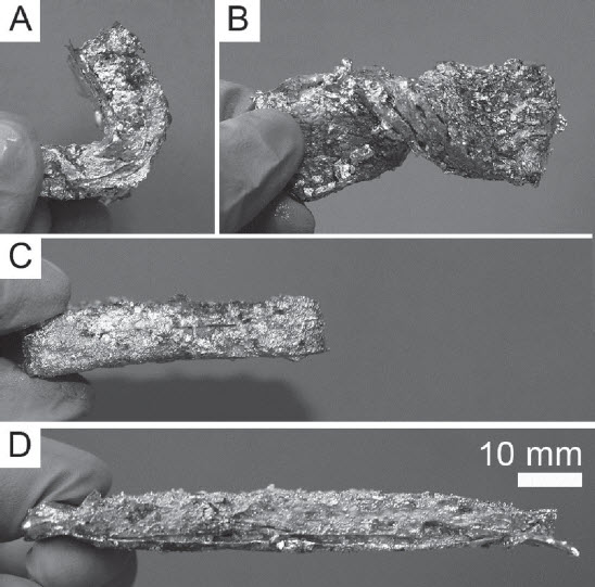
Morphed configurations that demonstrate the composite’s ability to hold bent (A), twisted (B), relaxed (C), and elongated (D) positions at room temperature (credit: Ilse M. Van Meerbeek et al./Advanced Materials)

Cornell University engineering professor Rob Shepherd and his group have developed a hybrid material combining a stiff metal called Field’s metal and a soft, porous silicone foam. Think T-1000 Terminator.

The material combines the best properties of both — stiffness when it’s called for, and elasticity when a change of shape is required. The material also has the ability to self-heal following damage.

“Sometimes you want a robot, or any machine, to be stiff,” said Shepherd. “But when you make them stiff, they can’t morph their shape very well. To give a soft robot both capabilities, to be able to morph their structure but also to be stiff and bear load, that’s what this material does.”

In addition to its low melting point of 144 degrees Fahrenheit, Field’s metal was chosen because, unlike similar alloys, it contains no lead, making it biocompatible.


Cornell University | Metal Elastomer Composite

To create the hybrid material, the elastomer foam is dipped into the molten metal, then placed in a vacuum so that the air in the foam’s pores is removed and replaced by the alloy. The foam had pore sizes of about 2 millimeters that can be tuned to create a stiffer or a more flexible material. In testing of its strength and elasticity, the material showed an ability to deform when heated above 144 degrees, regain rigidity when cooled, then return to its original shape and strength when reheated.

His group’s work has been published in Advanced Materials and will be the cover story in an upcoming issue of the journal’s print edition.

The work was supported by the U.S. Air Force Office of Scientific Research, the National Science Foundation, and the Alfred P. Sloan Foundation.


Abstract of Morphing Metal and Elastomer Bicontinuous Foams for Reversible Stiffness, Shape Memory, and Self-Healing Soft Machines

A metal–elastomer-foam composite that varies in stiffness, that can change shape and store shape memory, that self-heals, and that welds into monolithic structures from smaller components is presented.

A roadmap for the next generation of additive manufacturing materials and processes

The Strategic Roadmap for the Next Generation of Additive Manufacturing Materials offers a strategy for building the fundamental knowledge necessary to accelerate the design and application of additive manufacturing (AM) materials over the next 10 years. It organizes research and activities for developing additive manufacturing materials into five strategic thrusts: enabling integrated design methodologies for materials, processes and parts; developing AM process-structure-property relationships; establishing part and feedstock testing protocols; building AM process analytics capabilities; and exploring next-generation AM materials and processes. (credit: Penn State)

Penn State University researchers have released a roadmap for developing future additive manufacturing (3D printing) materials and processes.

It’s much needed. Most of the feedstock materials currently used in 3D printing are costly, not readily available, and limited, according to the researchers. The first additive manufacturing (AM) processes were actually developed 30 years ago. All of the metal alloys currently used, for example, were developed to be processed using casting and forging processes.

There is also a limited understating and inadequate compatibility with current AM processing technologies, the researchers say.

Funded by the U.S. National Institute of Standards and Technology, the new roadmap offers “a strategy for building the fundamental knowledge necessary to accelerate the design and application of additive manufacturing (AM) materials over the next 10 years.”

An example of a radical new additive-manufacturing process: JPL’s prototype of a compositionally graded mirror mount made by a new metal-based AM powder deposition technique. The gradient alloy component design — which contains a nickel and nickel-iron alloy at the top of the part and stainless steel at the base — replaces epoxy bonding techniques and mitigates the effects of thermal expansion caused by the extreme temperatures of outer space. (credit: NASA JPL)

The roadmapping effort involved more than 120 participants from industry, government and academia, according to Todd Palmer, Penn State associate professor of materials science and engineering and senior research associate with the Applied Research Lab (ARL), principal investigator on the roadmapping project.

The roadmap organizes research and activities into five strategic thrusts: enabling integrated design methodologies for materials, processes and parts; developing AM process-structure-property relationships; establishing part and feedstock testing protocols; building AM process analytics capabilities; and exploring next-generation AM materials and processes.

The researchers have also been coordinating their roadmapping efforts with America Makes, the National Additive Manufacturing Innovation Institute, which helps transition research and development in AM into the marketplace.

The researchers are also hoping that the roadmap generates enough interest from academia, research institutions, government labs, and industry partners so that they can launch the Consortium for Additive Manufacturing Materials (CAMM).

Additive manufacturing (3D printing) could affect a wide range of industries, including defense, energy, aerospace, automotive, medical and metals manufacturing.


editor’s comments: It will be interesting to see what cool new products, materials, and processes for the maker community become available. What would you make if you had the ideal 3D printer and ideal materials?


How to turn carbon dioxide into sustainable concrete

A sample of a new building material created to replace concrete (credit: UCLA Luskin)

A UCLA research team has developed a plan for capturing carbon from power-plant smokestacks (the largest source of harmful global greenhouse gas in the world) and use it to create a new building material — CO2NCRETE — that would be fabricated using 3D printers while replacing production of cement (which creates about 5 percent of the planet’s greenhouse gas emissions).

“I decided to get involved in this project because it could be a game-changer for climate policy,”  said J.R. DeShazo, professor of public policy at the UCLA Luskin School of Public Affairs and director of the UCLA Luskin Center for Innovation. “This technology tackles global climate change, which is one of the biggest challenges that society faces now and will face over the next century.”


UCLA Luskin School of Public Affairs | Carbon upcycling: Turning carbon dioxide into CO2NCRETE

DeShazo has provided the public policy and economic guidance for this research. The scientific contributions have been led by Gaurav Sant, associate professor and Henry Samueli Fellow in Civil and Environmental Engineering; Richard Kaner, distinguished professor in chemistry and biochemistry, and materials science and engineering; Laurent Pilon, professor in mechanical and aerospace engineering and bioengineering; and Matthieu Bauchy, assistant professor in civil and environmental engineering.

Beyond just capturing CO2

This isn’t the first attempt to capture carbon emissions from power plants. It’s been done before, but the challenge has been what to do with the carbon dioxide once it’s captured.

The researchers are excited about the possibility of reducing greenhouse gas in the U.S., especially in regions where coal-fired power plants are abundant. “But even more so is the promise to reduce the emissions in China and India,” DeShazo said. “China is currently the largest greenhouse gas producer in the world, and India will soon be number two, surpassing us.”

Thus far, the new construction material has been produced only at a lab scale, using 3-D printers to shape it into tiny cones. “We have proof of concept that we can do this,” DeShazo said. “But we need to begin the process of increasing the volume of material and then think about how to pilot it commercially.

“This technology could change the economic incentives associated with these power plants in their operations and turn the smokestack flue gas into a resource countries can use, to build up their cities, extend their road systems,” DeShazo said. “It takes what was a problem and turns it into a benefit in products and services that are going to be very much needed and valued in places like India and China.”


Abstract of Direct Carbonation of Ca(OH)2 Using Liquid and Supercritical CO2: Implications for Carbon-Neutral Cementation

By invoking analogies to lime mortars of times past, this study examines the carbonation of portlandite (Ca(OH)2) by carbon dioxide (CO2) in the liquid and supercritical states as a potential route toward CO2-neutral cementation. Portlandite carbonation is noted to be rapid; e.g., >80% carbonation of Ca(OH)2 is achieved in 2 h upon contact with liquid CO2 at ambient temperatures, and it is only slightly sensitive to the effects of temperature, pressure, and the state of CO2 over the range of 6 MPa ≤ p ≤ 10 MPa and 8 °C ≤ T ≤ 42 °C. Additional studies suggest that the carbonation of anhydrous ordinary portland cement is slower and far less reliable than that of portlandite. Although cementation is not directly assessed, detailed scanning electron microscopy (SEM) examinations of carbonated microstructures indicate that the carbonation products formed encircle and embed sand grains similar to that observed in lime mortars. The outcomes suggest innovative directions for “carbon-neutral cementation.”


Using machine learning to rationally design future electronics materials

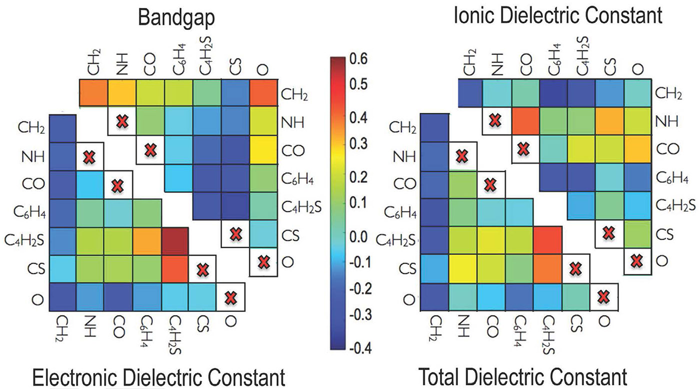
A schematic diagram of machine learning for materials discovery (credit: Chiho Kim, Ramprasad Lab, UConn)

Replacing inefficient experimentation, UConn researchers have used machine learning to systematically scan millions of theoretical compounds for qualities that would make better materials for solar cells, fibers, and computer chips.

Led by UConn materials scientist Ramamurthy ‘Rampi’ Ramprasad, the researchers set out to determine which polymer atomic configurations make a given polymer a good electrical conductor or insulator, for example.

A polymer is a large molecule made of many repeating building blocks. The most familiar example is plastics. What controls a polymer’s properties is mainly how the atoms in the polymer connect to each other. Polymers can also have diverse electronic properties. For example, they can be very good insulators or good conductors. And what controls all these properties is mainly how the atoms in the polymer connect to each other.

But with at least 95 stable elements, the number of possible combinations is astronomical. So they pared down the problem to a manageable subset. Many polymers are made of building blocks containing just a few atoms. They look like this:

Polyurea, a common plastic. In this diagram, N is nitrogen, H hydrogen, and O oxygen. R stands in for any number of chemicals that could slightly alter the polymer, but the repeating NH-O-NH-O is the basic structure. Most polymers look like that, made of carbon (C), H, N and O, with a few other elements thrown in occasionally. (credit: Yikrazuul/public domain)

For their project, Ramprasad’s group looked at polymers made of just seven building blocks: CH2, C6H4, CO, O, NH, CS, and C4H2S. These are found in common plastics such as polyethylene, polyesters, and polyureas. An enormous variety of polymers could theoretically be constructed using just these building blocks; Ramprasad’s group decided at first to analyze just 283, each composed of a repeated four-block unit.

They started from basic quantum mechanics, and calculated the three-dimensional atomic and electronic structures of each of those 283 four-block polymers (calculating the position of every electron and atom in a molecule with more than two atoms takes a powerful computer a significant chunk of time, which is why they did it for only 283 molecules).

Calculating key electronic properties

(credit: UConn)

Once they had the three-dimensional structures, they could calculate what they really wanted to know: each polymer’s properties.

  1. Ramprasad’s group calculated the band gap, which is the amount of energy it takes for an electron in the polymer to break free of its home atom and travel around the material; and the dielectric constant, which is a measure of the effect an electric field can have on the polymer. These properties translate to how much electric energy each polymer can store in itself.
  2. They then defined each polymer as a string of numbers, a sort of numerical fingerprint. Since there are seven possible building blocks, there are seven possible numbers, each indicating how many of each block type are contained in that polymer.
  3. But a simple number string like that doesn’t give enough information about the polymer’s structure, so they added a second string of numbers that tell how many pairs there are of each combination of building blocks, such as NH-O or C6H4-CS.
  4. Then they added a third string that described how many triples, like NH-O-CH2, there were. They arranged these strings as a three-dimensional matrix, which is a convenient way to describe such strings of numbers in a computer.
  5. Then they let the computer go to work. Using the library of 283 polymers they had laboriously calculated using quantum mechanics, the machine compared each polymer’s numerical fingerprint to its band gap and dielectric constant, and gradually ‘learned’ which building block combinations were associated with which properties. It could even map those properties onto a two-dimensional matrix of the polymer building blocks.
  6. Once the machine learned which atomic building block combinations gave which properties, it could accurately evaluate the band gap and dielectric constant for any polymer made of any combination of those seven building blocks, using just the numerical fingerprint of its structure.

Flow chart of the steps involved in the genetic algorithm (GA) approach, leading to direct design of polymers (credit: Arun Mannodi-Kanakkithodi et al/Scientific Reports)

Validating predictions

Many of the predictions of quantum mechanics and the machine learning scheme have been validated by Ramprasad’s UConn collaborators, who actually made several of the novel polymers and tested their properties.

The group published a paper on their polymer work in an open-access paper in Scientific Reports on Feb. 15; and another paper that utilizes machine learning in a different manner, namely, to discover laws that govern dielectric breakdown of insulators, will be published in a forthcoming issue of Chemistry of Materials.

You can see the predicted properties of every polymer Ramprasad’s group has evaluated in their online data vault, Khazana, which also provides their machine learning apps to predict polymer properties on the fly. They are also uploading data and the machine learning tools from their Chemistry of Materials work, and from an additional recent article published in Scientific Reports on Jan. 19 on predicting the band gap of perovskites, inorganic compounds used in solar cells, lasers, and light-emitting diodes.

Ramprasad’s work is aligned with a larger U.S. White House initiative called the Materials Genome Initiative. Much of Ramprasad’s work described here was funded by grants from the Office of Naval Research, as well as from the U.S. Department of Energy.


Abstract of Machine Learning Strategy for Accelerated Design of Polymer Dielectrics

The ability to efficiently design new and advanced dielectric polymers is hampered by the lack of sufficient, reliable data on wide polymer chemical spaces, and the difficulty of generating such data given time and computational/experimental constraints. Here, we address the issue of accelerating polymer dielectrics design by extracting learning models from data generated by accurate state-of-the-art first principles computations for polymers occupying an important part of the chemical subspace. The polymers are ‘fingerprinted’ as simple, easily attainable numerical representations, which are mapped to the properties of interest using a machine learning algorithm to develop an on-demand property prediction model. Further, a genetic algorithm is utilised to optimise polymer constituent blocks in an evolutionary manner, thus directly leading to the design of polymers with given target properties. While this philosophy of learning to make instant predictions and design is demonstrated here for the example of polymer dielectrics, it is equally applicable to other classes of materials as well.

Stretchable, flexible ‘meta-skin’ cloaks objects from radar at a range of frequencies

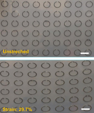
Flexible, stretchable, and frequency-tunable “meta-skin” can trap radar waves and cloak objects from radar detection (scale bars: 5 mm) (credit: Siming Yang et al./Scientific Reports)

Iowa State University engineers have developed a new flexible, stretchable, and  tunable “meta-skin” (metamaterial) “invisibility cloak” that uses rows of small liquid-metal devices to cloak an object from radar over a wide range of frequencies — and possibly at visible or infrared light ranges in the future.

First wraparound meta-skin (credit: Siming Yang et al./Scientific Reports)

The  skin has rows of split ring resonators embedded inside layers of silicone sheets. The resonators are filled with galinstan, a metal alloy that’s liquid at room temperature. That allows for stretching and flexing the polymer meta-skin, enabling it to be tuned to reduce reflection at a wide range of radar frequencies, unlike previous metamaterials.

Applications could include sub-wavelength imaging (of smaller objects), electromagnetic frequency tuning, shielding (from interference or detection), and scattering suppression (allowing a signal to be sent in specific directions rather than scattered).

Unlike conventional metamaterials, meta-skin can be conformed to curved and irregular surfaces.

The split-ring resonators used here are small rings with an outer radius of 2.5 millimeters and a thickness of half a millimeter. They have a 1 millimeter gap, essentially creating a small, curved segment of liquid wire.

The rings create electric inductors and the gaps create electric capacitors. Together they create a tuned resonator that can trap and suppress radar waves at a specific frequency. Stretching the meta-skin changes the size of the liquid metal rings inside and lowers the frequency the devices suppress.

Tests showed radar suppression was about 75 percent in the frequency range of 8 to 10 gigahertz in the experiment, according to the paper. When objects are wrapped in the meta-skin, the radar waves were suppressed in all incident directions and observation angles.

The open-access journal Scientific Reports recently reported the discovery online.

“The long-term goal is to shrink the size of these devices,” said senior author and associate professor Liang Dong, allowing for use with higher-frequency electromagnetic waves such as visible or infrared light. That would require advanced nanomanufacturing technologies and appropriate structural modifications, Dong noted.

The National Science Foundation and the China Scholarship Council partially supported the project.


Abstract of From Flexible and Stretchable Meta-Atom to Metamaterial: A Wearable Microwave Meta-Skin with Tunable Frequency Selective and Cloaking Effects

This paper reports a flexible and stretchable metamaterial-based “skin” or meta-skin with tunable frequency selective and cloaking effects in microwave frequency regime. The meta-skin is composed of an array of liquid metallic split ring resonators (SRRs) embedded in a stretchable elastomer. When stretched, the meta-skin performs as a tunable frequency selective surface with a wide resonance frequency tuning range. When wrapped around a curved dielectric material, the meta-skin functions as a flexible “cloaking” surface to significantly suppress scattering from the surface of the dielectric material along different directions. We studied frequency responses of multilayer meta-skins to stretching in a planar direction and to changing the spacing between neighboring layers in vertical direction. We also investigated scattering suppression effect of the meta-skin coated on a finite-length dielectric rod in free space. This meta-skin technology will benefit many electromagnetic applications, such as frequency tuning, shielding, and scattering suppression.

Converting atmospheric carbon dioxide into carbon nanotubes for use in batteries

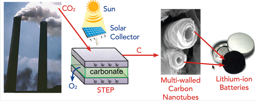
The Solar Thermal Electrochemical Process (STEP) converts atmospheric carbon dioxide into carbon nanotubes that can be used in advanced batteries. (credit: Julie Turner, Vanderbilt University)

The electric vehicle of the future will be carbon negative (reducing the amount of atmospheric carbon dioxide) not just carbon neutral (not adding CO2 to the atmosphere), say researchers at Vanderbilt University and George Washington University (GWU).

The trick: replace graphite electrodes in lithium-ion batteries (used in electric vehicles) with carbon nanotubes and carbon nanofibers recovered from carbon dioxide in the atmosphere. The new technology could also be used in sodium-ion batteries, currently under development for large-scale applications, such as the electric grid.

How to convert CO2 to carbon nanotubes

As described in an open-access paper in the Mar. 2 issue of the journal ACS Central Science, the project builds on a solar thermal electrochemical process (STEP) that can create carbon nanofibers from ambient carbon dioxide (see “‘Diamonds from the sky’ approach to turn CO2 into valuable carbon nanofibers“).

STEP uses solar energy to provide both the electrical and thermal energy needed to break down carbon dioxide into carbon and oxygen and to produce carbon nanotubes, which are stable, flexible, conductive and stronger than steel.

In lithium-ion batteries, the nanotubes replace the carbon anode used in commercial batteries. The team demonstrated that the carbon nanotubes gave a small boost to the performance, which was amplified when the battery was charged quickly.

In sodium-ion batteries, the researchers found that small defects in the carbon, which can be tuned using STEP, can unlock stable storage performance more than 3.5 times above that of sodium-ion batteries with graphite electrodes.

Both carbon-nanotube batteries were exposed to about 2.5 months of continuous charging and discharging and showed no sign of fatigue.

Depending on the specifications, making one of the two electrodes out of carbon nanotubes means that up to 40 percent of a battery could be made out of recycled CO2, according to Vanderbilt Assistant Professor of Mechanical Engineering Cary Pint, not including packaging (which could also be replaced in the future).

Cost benefits

This approach also reduces end-user battery cost, unlike most efforts to reuse CO2 aimed at low-valued fuels, like methanol, which “cannot justify the cost required to produce them,” Pint said.

“Other applications for the carbon nanotubes include carbon composites for strong, lightweight construction materials, sports equipment and car, truck and airplane bodies,” said GWU Professor of Chemistry Stuart Licht.

The researchers estimate that with a battery cost of $325 per kWh (the average cost of lithium-ion batteries reported by the Department of Energy in 2013), a kilogram of carbon dioxide has a value of about $18 as a battery material — six times more than when it is first converted to methanol — a number that increases when moving from large batteries used in electric vehicles to the smaller batteries used in electronics.

And unlike methanol, combining batteries with solar cells provides renewable power with zero greenhouse emissions.
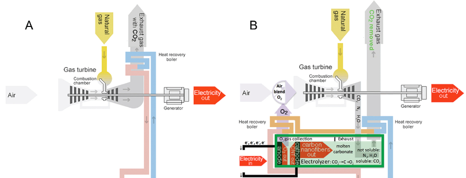
Comparison of conventional natural-gas plant (A), which has CO2 as an exhaust, with carbon nanofiber/carbon nanotube-based natural-gas plant (B) (steam turbine cooling/electricity-generating process (pink), common to both, omitted) (credit: Stuart Licht et al./ACS Central Science)

Licht also proposed that the STEP process could be coupled to a natural gas-powered electrical generator. The generator would provide electricity, heat, and a concentrated source of carbon dioxide that would boost the performance of the STEP process.

At the same time, the oxygen released in the process could be piped back to the generator, where it would boost the generator’s combustion efficiency to compensate for the amount of electricity that the STEP process consumes. The end result could be a fossil fuel electrical power plant with net-zero CO2 emissions.

The research was partially supported by National Science Foundation and NSF Graduate Research Fellowship grants.


Abstract of Carbon Nanotubes Produced from Ambient Carbon Dioxide for Environmentally Sustainable Lithium-Ion and Sodium-Ion Battery Anodes

The cost and practicality of greenhouse gas removal processes, which are critical for environmental sustainability, pivot on high-value secondary applications derived from carbon capture and conversion techniques. Using the solar thermal electrochemical process (STEP), ambient CO2 captured in molten lithiated carbonates leads to the production of carbon nanofibers (CNFs) and carbon nanotubes (CNTs) at high yield through electrolysis using inexpensive steel electrodes. These low-cost CO2-derived CNTs and CNFs are demonstrated as high performance energy storage materials in both lithium-ion and sodium-ion batteries. Owing to synthetic control of sp3 content in the synthesized nanostructures, optimized storage capacities are measured over 370 mAh g–1 (lithium) and 130 mAh g–1 (sodium) with no capacity fade under durability tests up to 200 and 600 cycles, respectively. This work demonstrates that ambient CO2, considered as an environmental pollutant, can be attributed economic value in grid-scale and portable energy storage systems with STEP scale-up practicality in the context of combined cycle natural gas electric power generation.
How to trigger self-powered mechanical movement

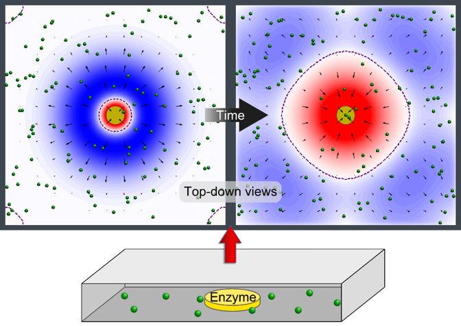
This animation illustrates an enzyme pump pushing particles away, then drawing them in. Initially, the flow pushes particles away from the pump (in the blue region). Later, the flow direction reverses and draws particles toward the pump (in the red region). (credit: University of Pittsburgh)

A new way to use the chemical reactions of certain enzymes to trigger self-powered mechanical movement has been developed by a team of researchers at Penn State University and the University of Pittsburgh.

These enzyme micropumps could be used for detecting substances, moving particles to build small structures, and delivering medications.

“One potential use is the release of insulin to a diabetes patient from a reservoir at a rate proportional to the concentration of glucose in the person’s blood,” said Ayusman Sen, Distinguished Professor of Chemistry at Penn State. “Another example is an enzyme pump that is triggered by nerve toxins to release an antidote agent to decontaminate and treat an exposed person.

The pumps provide precise control over flow rate without the aid of an external power source and are capable of turning on in response to specific chemicals in solution.

This image illustrates pumping in two directions at once with an enzyme patch. A patch of enzymes immobilized on a surface acts as a fluid pump. The fluid, and the small particles (green spheres) carried by the fluid, can simultaneously be pumped away from the patch (blue) in some parts of the chamber and toward the patch (red) in other locations. This behavior changes over time and is due to the changes in fluid density that the reaction produces. (credit: University of Pittsburgh)

A paper describing the team’s research was published last week in the journal Proceedings of the National Academy of Sciences. The team’s research was supported by the Charles E. Kauffman Foundation, the National Science Foundation, and the Defense Threat Reduction Agency.


Absract of Convective flow reversal in self-powered enzyme micropumps

Surface-bound enzymes can act as pumps that drive large-scale fluid flows in the presence of their substrates or promoters. Thus, enzymatic catalysis can be harnessed for “on demand” pumping in nano- and microfluidic devices powered by an intrinsic energy source. The mechanisms controlling the pumping have not, however, been completely elucidated. Herein, we combine theory and experiments to demonstrate a previously unreported spatiotemporal variation in pumping behavior in urease-based pumps and uncover the mechanisms behind these dynamics. We developed a theoretical model for the transduction of chemical energy into mechanical fluid flow in these systems, capturing buoyancy effects due to the solution containing nonuniform concentrations of substrate and product. We find that the qualitative features of the flow depend on the ratios of diffusivities δ=DP=DS and expansion coefficients β=βPS of the reaction substrate (S) and product (P). If δ>1 and δ>β (or if δ<1 and δ<β), an unexpected phenomenon arises: the flow direction reverses with time and distance from the pump. Our experimental results are in qualitative agreement with the model and show that both the speed and direction of fluid pumping (i) depend on the enzyme activity and coverage, (ii) vary with the distance from the pump, and (iii) evolve with time. These findings permit the rational design of enzymatic pumps that accurately control the direction and speed of fluid flow without external power sources, enabling effective, self-powered fluidic devices.

A practical solution to mass-producing low-cost nanoparticles

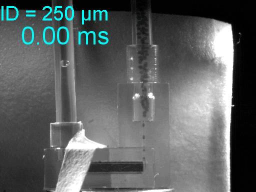
Nanoparticles form in a 3-D-printed microfluidic channel. Each droplet shown here is about 250 micrometers in diameter, and contains billions of platinum nanoparticles. (credit: Richard Brutchey and Noah Malmstadt/USC)

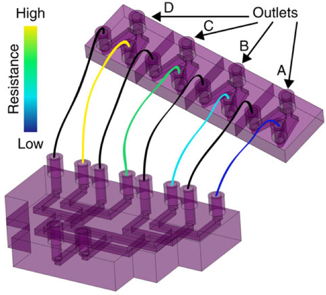
USC researchers have created an automated method of manufacturing nanoparticles that may transform the process from an expensive, painstaking, batch-by-batch process by a technician in a chemistry lab, mixing up a batch of chemicals by hand in traditional lab flasks and beakers.

Consider, for example, gold nanoparticles. Their ability to slip through the cell’s membrane makes them ideal delivery devices for medications to healthy cells, or fatal doses of radiation to cancer cells. But the price of gold nanoparticles at $80,000 per gram, compared to about $50 for pure raw gold goes.

The solution, published in an open access paper in Nature Communications on Feb. 23, is microfluidics — manipulating tiny droplets of fluid in narrow channels. The team 3D-printed tubes about 250 micrometers in diameter, possibly the smallest, fully enclosed 3D printed tubes anywhere.

Droplet formation for stable parallel microreactors (credit: Carson T. Riche et al./Nature Communications)

Then they built a parallel network of four of these tubes, side-by-side, and ran a combination of two non-mixing fluids (like oil and water) through them. As the two fluids fought to get out through the openings, they squeezed off tiny droplets. Each of these droplets acted as a microscale chemical reactor in which materials were mixed and nanoparticles were generated. Each microfluidic tube can create millions of identical droplets that perform the same reaction.

This sort of exotic process has been envisioned in the past, but its hasn’t been able to be scaled up because the parallel structure meant that if one tube got jammed, it would cause a ripple effect of changing pressures along its neighbors, knocking out the entire system.

The researchers bypassed this problem by altering the geometry of the tubes themselves, shaping the junction between the tubes such that the particles come out a uniform size and the system is immune to pressure changes.

The work was supported by the National Science Foundation.


USC | Nanoparticle Production


Abstract of Flow invariant droplet formation for stable parallel microreactors

The translation of batch chemistries onto continuous flow platforms requires addressing the issues of consistent fluidic behaviour, channel fouling and high-throughput processing. Droplet microfluidic technologies reduce channel fouling and provide an improved level of control over heat and mass transfer to control reaction kinetics. However, in conventional geometries, the droplet size is sensitive to changes in flow rates. Here we report a three-dimensional droplet generating device that exhibits flow invariant behaviour and is robust to fluctuations in flow rate. In addition, the droplet generator is capable of producing droplet volumes spanning four orders of magnitude. We apply this device in a parallel network to synthesize platinum nanoparticles using an ionic liquid solvent, demonstrate reproducible synthesis after recycling the ionic liquid, and double the reaction yield compared with an analogous batch synthesis.

Quantum dot solids: a new era in electronics?

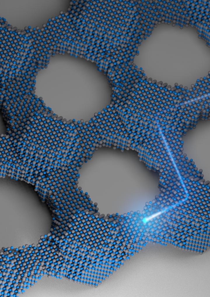
Connecting the dots: Playing ‘LEGO’ at the atomic scale to build atomically coherent quantum dot solids (credit: Kevin Whitham, Cornell University)

Just as the single-crystal silicon wafer forever changed the nature of communication 60 years ago, Cornell researchers hope their work with quantum dot solids — crystals made out of crystals — can help usher in a new era in electronics.

The team has fashioned two-dimensional superstructures out of single-crystal building blocks. Using a pair of chemical processes, the lead-selenium nanocrystals are synthesized into larger crystals, then fused together to form atomically coherent square superlattices.


Cornell University | Quantum dot solids

The difference between these and previous crystalline structures is the atomic coherence of each 5-nanometer crystal (a nanometer is one-billionth of a meter). They’re not connected by a substance between each crystal — they’re connected to each other directly. The electrical properties of these superstructures are potentially superior to existing semiconductor nanocrystals, with anticipated applications in energy absorption and light emission.

“As far as level of perfection, in terms of making the building blocks and connecting them into these superstructures, that is probably as far as you can push it,” said Tobias Hanrath, associate professor in the Robert Frederick Smith School of Chemical and Biomolecular Engineering, referring to the atomic-scale precision of the process.

The Hanrath group’s paper, “Charge transport and localization in atomically coherent quantum dot solids,” is published in this month’s issue of Nature Materials.

The strong coupling of the nanocrystals leads to formation of energy bands that can be manipulated based on the crystals’ makeup, and could be the first step toward discovering and developing other artificial materials with controllable electronic structure.

The structure of the Hanrath group’s superlattice, while superior to ligand-connected nanocrystal solids, still has multiple sources of disorder due to the fact that all nanocrystals are not identical. This creates defects, which limit electron wave function.

This work made use of the Cornell Center for Materials Research, which is supported by the National Science Foundation through its Materials Research Science and Engineering Center program. X-ray scattering was conducted at the Cornell High Energy Synchrotron Source, which is supported by the NSF and the National Institutes of Health.


Abstract of Charge transport and localization in atomically coherent quantum dot solids

Epitaxial attachment of quantum dots into ordered superlattices enables the synthesis of quasi-two-dimensional materials that theoretically exhibit features such as Dirac cones and topological states, and have major potential for unprecedented optoelectronic devices. Initial studies found that disorder in these structures causes localization of electrons within a few lattice constants, and highlight the critical need for precise structural characterization and systematic assessment of the effects of disorder on transport. Here we fabricated superlattices with the quantum dots registered to within a single atomic bond length (limited by the polydispersity of the quantum dot building blocks), but missing a fraction (20%) of the epitaxial connections. Calculations of the electronic structure including the measured disorder account for the electron localization inferred from transport measurements. The calculations also show that improvement of the epitaxial connections will lead to completely delocalized electrons and may enable the observation of the remarkable properties predicted for these materials.

Could ‘smart skin’ made of recyclable materials transform medicine and robotics?

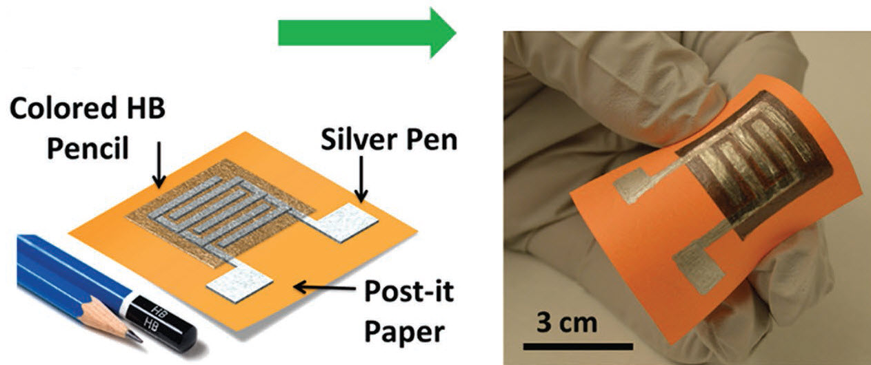
Capacitive-based disposable pH sensor. The silver pen could be replaced with aluminum foil. (credit: Joanna M. Nassar et al./Advanced Materials Technologies)

Here’s a challenge: using only low-cost materials available in your house (such as aluminum foil, pencil, scotch tape, sticky-notes, napkins, and sponges), build sensitive sensors (“smart skin”) for detecting temperature, humidity, pH, pressure, touch, flow, motion, and proximity (at a distance of 13 cm). Your sensors must show reliable and consistent results and be capable of connecting to low-cost, tiny computers such as Arduino and Raspberry Pi devices.

The goal here is to replace expensive manufacturing processes for creating paper-based sensors with a simple recyclable 3D stacked 6 × 6 “paper skin” array for simultaneous sensing, made solely from household resources, according to Muhammad Mustafa Hussain, senior author of an Advanced Materials Technologies journal open-access paper and professor at King Abdullah University of Science and Technology (KAUST) in Saudi Arabia.

How to create a temperature sensor

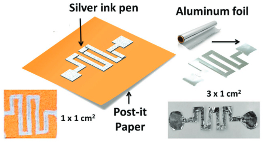
Schematic of temperature sensors using aluminum foil or silver ink pen (credit: Joanna M. Nassar/Advanced Materials Technologies)

Creating a highly sensitive temperature sensor requires just two things: a Post-It note and a piece of aluminum foil (a silver ink pen would be more sensitive).  A change of temperature would change the resistance of an aluminum strip. To measure the resistance change, connect the sensor to a highly sensitive ohmmeter, using an Arduino Uno, for example. (The output of the Arduino could trigger an alarm, for example.)

Arduino Uno and ohmmeter circuit. The sensor would replace the “resistor to be measured” in the schematic. The bottom resistor value would depend on the sensor resistance range. (credit: Adafruit and Learning About Electronics)

 Two designs for a simple pressure sensor

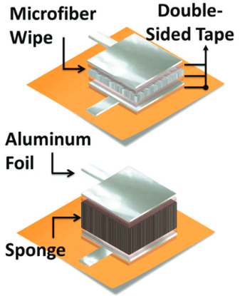
Two designs for a pressure sensor using a parallel-plate structure: (top) Microfiber wipe and sponge; (bottom) more sensitive air-gap structure with sponge. As applied pressure increases, the dielectric thickness decreases, increasing the output capacitance. To measure it, the aluminum foil is connected to a resistor–capacitor circuit (RC circuit), which is connected to an Arduino or Raspberry Pi device to calculate associated pressure change. (credit: Joanna M. Nassar et al./Advanced Materials Technologies)

The simple fabrication process and low-cost materials used “make this flexible platform the lowest cost and accessible to anyone, without affecting performance in terms of response and sensitivity,” Hussain says.

“Democratization of electronics will be key in the future for its continued growth. … This is the first time a [single] platform shows multi-sensory functionalities close to that of natural skin.”


Abstract of Paper Skin Multisensory Platform for Simultaneous Environmental Monitoring

Human skin and hair can simultaneously feel pressure, temperature, humidity, strain, and flow—great inspirations for applications such as artificial skins for burn and acid victims, robotics, and vehicular technology. Previous efforts in this direction use sophisticated materials or processes. Chemically functionalized, inkjet printed or vacuum-technology-processed papers albeit cheap have shown limited functionalities. Thus, performance and/or functionalities per cost have been limited. Here, a scalable “garage” fabrication approach is shown using off-the-shelf inexpensive household elements such as aluminum foil, scotch tapes, sticky-notes, napkins, and sponges to build “paper skin” with simultaneous real-time sensing capability of pressure, temperature, humidity, proximity, pH, and flow. Enabling the basic principles of porosity, adsorption, and dimensions of these materials, a fully functioning distributed sensor network platform is reported, which, for the first time, can sense the vitals of its carrier (body temperature, blood pressure, heart rate, and skin hydration) and the surrounding environment.