‘Eternal 5D’ data storage could reliably record the history of humankind

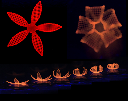
Documents captured in nanostructured glass, expected to last billions of years (credit: University of Southampton)

Scientists at the University of Southampton Optoelectronics Research Centre (ORC) have developed the first digital data storage system capable of creating archives that can survive for billions of years.

Using nanostructured glass, the system has 360 TB per disc capacity, thermal stability up to 1,000°C, and virtually unlimited lifetime at room temperature (or 13.8 billion years at 190°C ).

As a “highly stable and safe form of portable memory,” the technology opens up a new era of “eternal” data archiving that could be essential to cope with the accelerating amount of information currently being created and stored, the scientists says.* The system could be especially useful for organizations with big archives, such as national archives, museums, and libraries, according to the scientists.

Superman memory crystal

5D optical storage writing setup. FSL: femtosecond laser; SLM: spatial light modulator; FL1 and FL2: Fourier lens; HPM: half-wave plate matrix; AP: aperture; WIO: water immersion objective. Inset: Linearly polarized light (white arrows) with different intensity levels propagate simultaneously through each half-wave plate segment with different slow-axis orientation (black arrows). The colors of the rectangle indicate four different intensity levels. (credit: University of Southampton)

The recording system uses an ultrafast laser to produce extremely short (femtosecond) and intense pulses of light. The file is written in three up to 18 layers of nanostructured dots separated by five micrometers (one millionth of a meter) in fuzed quartz (coined as a “Superman memory crystal” (as in “memory crystals” used in the Superman films).” The self-assembled nanostructures change the way light travels through glass, modifying the polarization of light, which can then be read by a combination optical microscope and polarizer, similar to that found in Polaroid sunglasses.

The recording method is described as “5D” because the information encoding is in five dimensions — three-dimensional position plus size and orientation.

So far, the researchers have saved major documents from human history, such as the Universal Declaration of Human Rights (UDHR), Newton’s Opticks, Magna Carta, and Kings James Bible as digital copies. A copy of the UDHR encoded to 5D data storage was recently presented to UNESCO by the ORC at the International Year of Light (IYL) closing ceremony in Mexico.

The team is now looking for industry partners to further develop and commercialize this technology.

The researchers will present their research at the photonics industry’s SPIE (the International Society for Optical Engineering Conference) in San Francisco on Wednesday Feb. 17.

* In 2008, the International Data Corporation [found] that total capacity of data stored is increasing by around 60% each year. As a result, more than 39,000 exabytes of data will be generated by 2020. This amount of data will cause a series of problems and one of the main will be power consumption. 1.5% of the total U.S. electricity consumption in 2010 was given to the data centers in the U.S. According to a report by the Natural Resources Defence Council, the power consumption of all data centers in the U.S. will reach roughly 140 billion kilowatt-hours per each year by 2020. This amount of electricity is equivalent to that generated by roughly thirteen Heysham 2 nuclear power stations (one of the biggest stations in UK, net 1240 MWe).

Most of these data centers are built based on hard-disk drive (HDD), with only a few designed on optical discs. HDD is the most popular solution for digital data storage according to the International Data Corporation. However, HDD is not an energy-efficient option for data archiving; the loading energy consumption is around 0.04 W/GB. In addition, HDD is an unsatisfactory candidate for long-term storage due to the short lifetime of the hardware and requires transferring data every two years to avoid any loss.

— Jingyu Zhang et al. Eternal 5D data storage by ultrafast laser writing in glass. Proceedings of the SPIE OPTO 2016


Abstract of Eternal 5D data storage by ultrafast laser writing in glass

Femtosecond laser writing in transparent materials has attracted considerable interest due to new science and a wide range of applications from laser surgery, 3D integrated optics and optofluidics to geometrical phase optics and ultra-stable optical data storage. A decade ago it has been discovered that under certain irradiation conditions self-organized subwavelength structures with record small features of 20 nm, could be created in the volume of silica glass. On the macroscopic scale the self-assembled nanostructure behaves as a uniaxial optical crystal with negative birefringence. The optical anisotropy, which results from the alignment of nano-platelets, referred to as form birefringence, is of the same order of magnitude as positive birefringence in crystalline quartz. The two independent parameters describing birefringence, the slow axis orientation (4th dimension) and the strength of retardance (5th dimension), are explored for the optical encoding of information in addition to three spatial coordinates. The slow axis orientation and the retardance are independently manipulated by the polarization and intensity of the femtosecond laser beam. The data optically encoded into five dimensions is successfully retrieved by quantitative birefringence measurements. The storage allows unprecedented parameters including hundreds of terabytes per disc data capacity and thermal stability up to 1000°. Even at elevated temperatures of 160oC, the extrapolated decay time of nanogratings is comparable with the age of the Universe – 13.8 billion years. The demonstrated recording of the digital documents, which will survive the human race, including the eternal copies of Kings James Bible and Magna Carta, is a vital step towards an eternal archive.

A black hole on a chip made of a metal that behaves like water

In a new paper published in Science, researchers at the Harvard and Raytheon BBN Technology have observed, for the first time, electrons in a metal behaving like a fluid (credit: Peter Allen/Harvard SEAS)

A radical discovery by researchers at Harvard and Raytheon BBN Technology about graphene’s hidden properties could lead to a model system to explore exotic phenomena like black holes and high-energy plasmas, as well as novel thermoelectric devices.

In a paper published Feb. 11 in Science, the researchers document their discovery of electrons in graphene behaving like a fluid. To make this observation, the team improved methods to create ultra-clean graphene* and developed a new way to measure its thermal conductivity.

A black hole on a chip

In ordinary 3D metals, electrons hardly interact with each other. But graphene’s two-dimensional, honeycomb structure acts like an electron superhighway in which all the particles have to travel in the same lane. The electrons in this ultra-clean graphene act like massless relativistic objects, some with positive charge and some with negative charge.

They move at incredible speed — 1/300 of the speed of light — and have been predicted to collide with each other ten trillion times a second at room temperature.  These intense interactions between charge particles have never been observed in an ordinary metal before.

Most of our world is described by classical physics. But very small things, like electrons, are described by quantum mechanics while very large and very fast things, like galaxies, are described by relativistic physics, pioneered by Albert Einstein.

Combining these different sets of laws of physics is notoriously difficult, but there are extreme examples where they overlap. High-energy systems like supernovas and black holes can be described by linking classical theories of hydrodynamics with Einstein’s theories of relativity.

A quantum ‘Dirac’ fluid metal

But since we can’t run an experiment on a black hole (yet), enter graphene.

When the strongly interacting particles in graphene were driven by an electric field, they behaved not like individual particles but like a fluid that could be described by hydrodynamics.

“Physics we discovered by studying black holes and string theory, we’re seeing in graphene,” said Andrew Lucas, co-author and graduate student with Subir Sachdev, the Herchel Smith Professor of Physics at Harvard. “This is the first model system of relativistic hydrodynamics in a metal.”

Industrial implications

A small chip of graphene could also be used to model the fluid-like behavior of other high-energy systems.

To observe the hydrodynamic system, the team turned to noise. At finite temperature, the electrons move about randomly:  the higher the temperature, the noisier the electrons. By measuring the temperature of the electrons to three decimal points, the team was able to precisely measure the thermal conductivity of the electrons.

“This work provides a new way to control the rate of heat transduction in graphene’s electron system, and as such will be key for energy and sensing-related applications,” said Leonid Levitov, professor of physics at MIT.

“Converting thermal energy into electric currents and vice versa is notoriously hard with ordinary materials,” said Lucas. “But in principle, with a clean sample of graphene there may be no limit to how good a device you could make.”

The research was led by Philip Kim, professor of physics and applied physics at The Harvard John A. Paulson School of Engineering and Applied Sciences (SEAS).

* The team created an ultra-clean sample by sandwiching the one-atom thick graphene sheet between tens of layers of an electrically insulating perfect transparent crystal with a similar atomic structure of graphene.

“If you have a material that’s one atom thick, it’s going to be really affected by its environment,” said Jesse Crossno, a graduate student in the Kim Lab and first author of the paper. “If the graphene is on top of something that’s rough and disordered, it’s going to interfere with how the electrons move. It’s really important to create graphene with no interference from its environment.”

Next, the team set up a kind of thermal soup of positively charged and negatively charged particles on the surface of the graphene, and observed how those particles flowed as thermal and electric currents.


Harvard John A. Paulson School of Engineering and Applied Sciences | How to Make Graphene


Abstract of Observation of the Dirac fluid and the breakdown of the Wiedemann-Franz law in graphene

Interactions between particles in quantum many-body systems can lead to collective behavior described by hydrodynamics. One such system is the electron-hole plasma in graphene near the charge neutrality point, which can form a strongly coupled Dirac fluid. This charge neutral plasma of quasi-relativistic fermions is expected to exhibit a substantial enhancement of the thermal conductivity, thanks to decoupling of charge and heat currents within hydrodynamics. Employing high sensitivity Johnson noise thermometry, we report an order of magnitude increase in the thermal conductivity and the breakdown of the Wiedemann-Franz law in the thermally populated charge neutral plasma in graphene. This result is a signature of the Dirac fluid, and constitutes direct evidence of collective motion in a quantum electronic fluid.

Graphene is ideal substrate for brain electrodes, researchers find

This illustration portrays neurons interfaced with a sheet of graphene molecules in the background (credit: Graphene Flagship)

An international study headed by the European Graphene Flagship research consortium has found that graphene is a promising material for use in electrodes that interface with neurons, based on its excellent conductivity, flexibility for molding into complex shapes, biocompatibility, and stability within the body.

The graphene-based substrates they studied* promise to overcome problems with “glial scar” tissue formation (caused by electrode-based brain trauma and long-term inflammation). To avoid that, current electrodes based on tungsten or silicon use a protective coating on electrodes, which reduces charge transfer. Current electrodes are also rigid (resulting in tissue detachment and preventing neurons from moving) and generate electrical noise, with partial or complete loss of signal over time, the researchers note in a paper published recently in the journal ACS Nano.

Electrodes are used as neural biosensors and for prosthetic applications — such as deep-brain intracranial electrodes used to control motor disorders (mainly epilepsy or Parkinson’s) and for brain-computer interfaces (BCIs), used to recover sensory functions or control robotic arms for paralyzed patients. These applications require an interface with long-term, minimal interference.

Interfacing graphene to neurons directly

Scanning electron microscope image of rat hippocampal neurons grown in the lab on a graphene-based substrate, showing normal morphology characterized by well-defined round neural soma, extended neurite arborization (branching), and cell density similar to control substrates (credit: A. Fabbro et al./ACS Nano)

“For the first time, we interfaced graphene to neurons directly, without any peptide-coating,” explained lead neuroscientist Prof. Laura Ballerini of the International School for Advanced Studies (SISSA/ISAS) and the University of Trieste.

Using electron microscopy and immunofluorescence, the researchers found that the neurons remained healthy, transmitting normal electric impulses and, importantly, no adverse glial reaction, which leads to damaging scar tissue, was seen.

Atomic force microscope (AFM) image of graphene-based substrate created using liquid phase exfoliation (credit: A. Fabbro et al./ACS Nano)

As a next step, Ballerini says the team plans to investigate how different forms of graphene, from multiple layers to monolayers, are able to affect neurons,  and “whether tuning the graphene material properties might alter the synapses and neuronal excitability in new and unique ways.”

Prof. Andrea C. Ferrari, Director of the Cambridge Graphene Centre and Chair of the Graphene Flagship Executive Board, said the Flagship will “support biomedical research and development based on graphene technology with a new work package and a significant cash investment from 2016.”

The interdisciplinary collaboration also included the University Castilla-La Mancha and the Cambridge Graphene Centre.

* The study used two methods of creating graphene-based substrates (GBSs).  Liquid phase exfoliation (LPE) — peeling off graphene from graphite — can be performed without the potentially hazardous chemical treatments involved in graphene oxide production, is scalable, and operates at room temperature, with high yield. LPE dispersions can also be easily deposited on target substrates by drop-casting, filtration, or printing. Ball milling (BM), with the help of melamine (which forms large hydrogen-bond domains, unlike LPE), can be performed in a solid environment. “Our data indicate that both GBSs are promising for next-generation bioelectronic systems, to be used as brain interfaces,” the paper concludes.

A new technique for super-resolution digital microscopy

The image sensor of the wavelength scanning super-resolution apparatus collects a “stack” of images of the sample (credit: Ozcan Lab)

Researchers from the California NanoSystems Institute at UCLA have created a new technique using lens-free holograms that greatly enhances digital microscopy images, which are sometimes blurry and pixelated.

The new technique, called “wavelength scanning pixel super-resolution,” uses a device that captures a stack of digital images of the same specimen, each with a slightly different wavelength of light. Then, researchers apply a newly devised algorithm that divides the pixels in each captured image into a number of smaller pixels, resulting in a much higher-resolution digital image of the specimen.

The research team was led by Aydogan Ozcan, Chancellor’s Professor of Electrical Engineering and Bioengineering at the UCLA Henry Samueli School of Engineering and Applied Science. The study appears in an open-access paper in the journal Light: Science and Applications, published by the Nature Publishing Group.

Raw data is transformed into a super-resolution image (credit: Ozcan Lab)

Faster, more-accessible diagnosis

“These results mean we can see and inspect large samples with finer details at the sub-micron [nanoscale] level,” Ozcan said. “We have applied this method to lens-based conventional microscopes, as well as our lensless on-chip microscopy systems that create microscopic images using holograms, and it works across all these platforms.”

The benefits of this new method are wide-ranging, but especially significant in pathology, where rapid microscopic imaging of large numbers of tissue or blood cells is key to diagnosing diseases such as cancer. The specimens used in the study were blood samples, used to screen for various diseases, and Papanicolaou tests, which are used to screen for cervical cancer.

Ozcan said that wavelength scanning super-resolution works on both colorless and dye-stained samples. The entire apparatus fits on a desktop, so its size and convenience could be of great benefit to doctors and scientists using microscopes in resource-limited settings such as clinics in developing countries.

The research was supported by the Presidential Early Career Award for Scientists and Engineers, the Army Research Office, the National Science Foundation, the Office of Naval Research and the Howard Hughes Medical Institute.


Abstract of Pixel super-resolution using wavelength scanning

Undersampling and pixelation affect a number of imaging systems, limiting the resolution of the acquired images, which becomes particularly significant for wide-field microscopy applications. Various super-resolution techniques have been implemented to mitigate this resolution loss by utilizing sub-pixel displacements in the imaging system, achieved, for example, by shifting the illumination source, the sensor-array and/or the sample, followed by digital synthesis of a smaller effective pixel by merging these subpixel-shifted low-resolution images. Herein, we introduce a new pixel super-resolution method that is based on wavelength scanning and demonstrate that as an alternative to physical shifting/displacements, wavelength diversity can be used to boost the resolution of a wide-field imaging system and significantly increase its space-bandwidth product. We confirmed the effectiveness of this new technique by improving the resolution of lens-free as well as lens-based microscopy systems and developed an iterative algorithm to generate high-resolution reconstructions of a specimen using undersampled diffraction patterns recorded at a few wavelengths covering a narrow spectrum (10-30 nm). When combined with a synthetic-aperture-based diffraction imaging technique, this wavelength-scanning super-resolution approach can achieve a half-pitch resolution of 250 nm, corresponding to a numerical aperture of approximately 1.0, across a large field of view (>20 mm2 ). We also demonstrated the effectiveness of this approach by imaging various biological samples, including blood and Papanicolaou smears. Compared with displacement-based super-resolution techniques, wavelength scanning brings uniform resolution improvement in all directions across a sensor array and requires significantly fewer measurements. This technique would broadly benefit wide-field imaging applications that demand larger space-bandwidth products.

A flexible, transparent pressure sensor

Pressure sensors wrap around and conform to the shape of the fingers while still accurately measuring pressure distribution. (credit: 2016 Someya Laboratory)

Doctors may one day be able to physically screen for breast cancer using pressure-sensitive rubber gloves to detect tumors, thanks to a transparent, bendable, and sensitive pressure sensor newly developed by Japanese and American teams.

Conventional pressure sensors can’t measure pressure changes accurately once they are twisted or wrinkled, making them unsuitable for use on complex and moving surfaces, and they can’t be miniaturized below 100 micrometers (0.1 millimeters) thickness because of limitations in current production methods.

To address these issues, an international team of researchers led by Dr. Sungwon Lee and Professor Takao Someya of the University of Tokyo’s Graduate School of Engineeringhas developed a nanofiber-type pressure sensor made from carbon nanotubes and graphene that can measure pressure distribution of rounded surfaces such as an inflated balloon and maintain its sensing accuracy even when bent over a radius of 80 micrometers, equivalent to just twice the width of a human hair. The sensor is roughly 8 micrometers thick and can measure the pressure in 144 locations at once.

The device demonstrated in this study consists of organic transistors, electronic switches made from carbon and oxygen-based organic materials, and a pressure-sensitive nanofiber structure. Carbon nanotubes and graphene were added to an elastic polymer to create nanofibers with a diameter of 300 to 700 nanometers, which were then entangled with each other to form a transparent, thin and light porous structure.

The material may also have applications in improving the touch sensitivity in robots.


Abstract of A transparent bending-insensitive pressure sensor

Measuring small normal pressures is essential to accurately evaluate external stimuli in curvilinear and dynamic surfaces such as natural tissues. Usually, sensitive and spatially accurate pressure sensors are achieved through conformal contact with the surface; however, this also makes them sensitive to mechanical deformation (bending). Indeed, when a soft object is pressed by another soft object, the normal pressure cannot be measured independently from the mechanical stress. Here, we show a pressure sensor that measures only the normal pressure, even under extreme bending conditions. To reduce the bending sensitivity, we use composite nanofibres of carbon nanotubes and graphene. Our simulations show that these fibres change their relative alignment to accommodate bending deformation, thus reducing the strain in individual fibres. Pressure sensitivity is maintained down to a bending radius of 80 μm. To test the suitability of our sensor for soft robotics and medical applications, we fabricated an integrated sensor matrix that is only 2 μm thick. We show real-time (response time of ∼20 ms), large-area, normal pressure monitoring under different, complex bending conditions.

A novel ’4D printing’ method inspired by plants

This series of images shows the transformation (top right) of a 4D-printed hydrogel composite structure (top left) after its submersion (bottom) in water (credit: Wyss Institute at Harvard University)

Harvard University scientists have evolved their microscale 3D printing technology to the fourth dimension, time. Inspired by natural structures like plants, which respond and change their form over time according to environmental stimuli, the team has designed 4D-printed hydrogel composite structures that change shape upon immersion in water.

The team is located at the Wyss Institute for Biologically Inspired Engineering at Harvard University and the Harvard John A. Paulson School of Engineering and Applied Sciences.

“This work represents an elegant advance in programmable materials assembly, made possible by a multidisciplinary approach,” said Jennifer Lewis, Sc.D., senior author of a new study reported on January 25 in a new  in Nature Materials. “We have now gone beyond integrating form and function to create transformable architectures.”

In nature, flowers and plants have tissue compositions and microstructures that result in dynamic morphologies (forms) that change according to their environments. Mimicking the variety of shape changes undergone by plant organs such as tendrils, leaves, and flowers in response to environmental stimuli like humidity and/or temperature, the 4D-printed hydrogel composites developed by Lewis and her team are programmed to contain precise, localized swelling behaviors.

Derived from wood

The trick: the hydrogel composites contain cellulose fibrils that are derived from wood and are similar to the microstructures that enable shape changes in plants.

By aligning cellulose fibrils during printing, the hydrogel composite ink is encoded with anisotropic swelling and stiffness, which can be patterned to produce intricate shape changes. The anisotropic (irregular) nature of the cellulose fibrils gives rise to varied directional properties that can be predicted and controlled. That’s why wood can be split easier along the grain rather than across it.

Likewise, when immersed in water, the hydrogel-cellulose fibril ink undergoes differential swelling behavior along and orthogonal to the printing path. Combined with a proprietary mathematical model developed by the team that predicts how a 4D object must be printed to achieve prescribed transformable shapes, the new method opens up many new and exciting potential applications for 4D printing technology including smart textiles, soft electronics, biomedical devices, and tissue engineering.

The composite ink that the team uses flows like liquid through the printhead, yet rapidly solidifies once printed. A variety of hydrogel materials can be used interchangeably resulting in different stimuli-responsive behaviors, while the cellulose fibrils can be replaced with other anisotropic fillers of choice, including conductive fillers.

Complex flower morphologies generated by biomimetic 4D printing. A flower demonstrating a range of morphologies inspired by a native orchid, the Dendrobium helix (courtesy of Ricardo Valentin). Based on the print path, this orchid architecture exhibits four different configurations: bending, twisting and ruffling corolla surrounding the central funnel-like domain (scale bars, 5 mm). (credit: A. Sydney Gladman et al./Nature Materials)

The mathematical model prescribes the printing pathways required to achieve the desired shape-transforming response. Specifically, it solves the “inverse problem” — the challenge of being able to predict what the printing toolpath must be to encode swelling behaviors toward achieving a specific desired target shape.

“It is wonderful to be able to design and realize, in an engineered structure, some of nature’s solutions,” said L. Mahadevan, Ph.D., a Wyss Core Faculty member as well as the Lola England de Valpine Professor of Applied Mathematics, Professor of Organismic and Evolutionary Biology, and Professor of Physics at Harvard University and Harvard SEAS, is a co-author on the study. “By solving the inverse problem, we are now able to reverse-engineer the problem and determine how to vary local inhomogeneity, i.e. the spacing between the printed ink filaments, and the anisotropy, i.e. the direction of these filaments, to control the spatiotemporal response of these shapeshifting sheets.”

Lewis is a Core Faculty member at the Wyss Institute for Biologically Inspired Engineering at Harvard University and the Hansjörg Wyss Professor of Biologically Inspired Engineering at the Harvard John A. Paulson School of Engineering and Applied Science (SEAS). Their team also includes co-author, Ralph Nuzzo, Ph.D., the G.L. Clark Professor of Chemistry at the University of Illinois at Urbana-Champaign.


Wyss Institute | 4D Printing: Shapeshifting Architectures


Abstract of Biomimetic 4D printing

Shape-morphing systems can be found in many areas, including smart textiles, autonomous robotics, biomedical devices, drug delivery and tissue engineering. The natural analogues of such systems are exemplified by nastic plant motions, where a variety of organs such as tendrils, bracts, leaves and flowers respond to environmental stimuli (such as humidity, light or touch) by varying internal turgor, which leads to dynamic conformations governed by the tissue composition and microstructural anisotropy of cell walls. Inspired by these botanical systems, we printed composite hydrogel architectures that are encoded with localized, anisotropic swelling behaviour controlled by the alignment of cellulose fibrils along prescribed four-dimensional printing pathways. When combined with a minimal theoretical framework that allows us to solve the inverse problem of designing the alignment patterns for prescribed target shapes, we can programmably fabricate plant-inspired architectures that change shape on immersion in water, yielding complex three-dimensional morphologies.

How to make almost any shape out of a flat sheet of paper

Mahadevan and his team have characterized a fundamental origami fold, or tessellation, that could be used as a building block to create almost any three-dimensional shape, as seen above (credit: Mahadevan Lab/Harvard SEAS)

Harvard scientist L. Mahadevan and his team have devised a way to make virtually any shape out of a flat sheet of paper, using a fundamental origami or tessellation fold.

The folding pattern, known as the Miura-ori, is a periodic way to tile the plane using the simplest mountain-valley fold in origami. It was used as a decorative item in clothing at least as long ago as the 15th century. A folded Miura can be packed into a flat, compact shape and unfolded in one continuous motion, making it ideal for packing rigid structures like solar panels.  It also occurs in nature in a variety of situations, such as in insect wings and certain leaves.

Mahadevan suggests that this simple folding pattern could serve as a template for more complicated shapes, such as space-bound payloads, surgical stents that can be packed flat and pop-up into three-dimensional structures once inside the body, or dining room tables that can lean flat against the wall until they are ready to be used.

To explore the potential of the tessellation, the team developed an algorithm that can create certain shapes using the Miura-ori fold, repeated with small variations. Given the specifications of the target shape, the program lays out the folds needed to create the design, which can then be laser printed for folding.

The program takes into account several factors, including the stiffness of the folded material and the trade-off between the accuracy of the pattern and the effort associated with creating finer folds — an important characterization because, as of now, these shapes are all folded by hand.

This spiral folds rigidly from flat pattern through the target surface and onto the flat-folded plane (credit: Mahadevan Lab)

“Essentially, we would like to be able to tailor any shape by using an appropriate folding pattern,” said Mahadevan. “Starting with the basic mountain-valley fold, our algorithm determines how to vary it by gently tweaking it from one location to the other to make a vase, a hat, a saddle, or to stitch them together to make more and more complex structures.”

“The really exciting thing about this fold is it is completely scalable.You can do this with graphene, which is one atom thick, or you can do it on the architectural scale.”

Mahadevan is the Lola England de Valpine Professor of Applied Mathematics, Organismic and Evolutionary Biology, and Physics at the Harvard John A. Paulson School of Engineering and Applied Sciences (SEAS). He is also a core faculty member of the Wyss Institute for Biologically Inspired Engineering, and member of the Kavli Institute for Bionano Science and Technology, at Harvard University.

The research is published in Nature Materials.


Abstract of Programming curvature using origami tessellations

Origami describes rules for creating folded structures from patterns on a flat sheet, but does not prescribe how patterns can be designed to fit target shapes. Here, starting from the simplest periodic origami pattern that yields one-degree-of-freedom collapsible structures—we show that scale-independent elementary geometric constructions and constrained optimization algorithms can be used to determine spatially modulated patterns that yield approximations to given surfaces of constant or varying curvature. Paper models confirm the feasibility of our calculations. We also assess the difficulty of realizing these geometric structures by quantifying the energetic barrier that separates the metastable flat and folded states. Moreover, we characterize the trade-off between the accuracy to which the pattern conforms to the target surface, and the effort associated with creating finer folds. Our approach enables the tailoring of origami patterns to drape complex surfaces independent of absolute scale, as well as the quantification of the energetic and material cost of doing so.

How to modify a 3-D printer to print high-performance products

Ultrasonic waves form microscopic glass fibers into a pattern of lines, collectively creating a reinforcing microstructure that gives the printed component increased strength. (credit: Tom Llewellyn-Jones, Bruce Drinkwater and Richard Trask)

University of Bristol engineers have developed a new type of 3-D printing that can print strong composite materials.

The new method is based on a modification of an off-the-shelf 3D printer: mounting a switchable, focused laser module and an ultrasonic alignment apparatus.

The method uses ultrasonic waves to position and align millions of microscopic glass fibers to form reinforcement fibers into a framework that gives the material strength. A focused laser beam carriage then cures (hardens) the epoxy resin for printing. The precise orientation of the fibers can be controlled by switching the ultrasonic standing-wave pattern mid-print. The engineers achieved a print speed of 20 millimeters per second, similar to conventional additive layer techniques.

Schematic representation of printer and ultrasonic manipulation rig. (a) Switchable laser module (red) is attached to the print head carriage (gray) and traces out the shape of the printed part. The laser can be deliberately defocused to cure large regions slowly by increasing the height of the laser module. (b) Focused laser beam (blue) cures resin within the cavity of the ultrasonic manipulation device (red). LD=laser diode, P=PMMA, W=Water, PZT=lead zirconate titanate transducers, R=resin. Cross sections of the bundles of glass fibers lying within traps are shown, separated by half a wavelength of the laser light. (credit: Thomas M. Llewellyn-Jones et al./Smart Materials and Structures)

Composite materials are widely used in many high-performance products such as tennis rackets, golf clubs, and airplanes. So this technology should soon enable a much greater range of strong composite materials to be 3-D printed at home and at low cost, the engineers suggest. The method is expected to be useful for a range of smart materials applications, such as printing resin-filled capsules for self-healing materials or piezoelectric particles for energy harvesting.

The study is described in an open-access paper in Smart Materials and Structures.


Matt Sutton, Tom Llewellyn-Jones, Bruce Drinkwater and Richard Trask | The new composite printing process. 


Abstract of 3D printed components with ultrasonically arranged microscale structure

This paper shows the first application of in situ manipulation of discontinuous fibrous structure mid-print, within a 3D printed polymeric composite architecture. Currently, rapid prototyping methods (fused filament fabrication, stereolithography) are gaining increasing popularity within the engineering community to build structural components. Unfortunately, the full potential of these components is limited by the mechanical properties of the materials used. The aim of this study is to create and demonstrate a novel method to instantaneously orient micro-scale glass fibres within a selectively cured photocurable resin system, using ultrasonic forces to align the fibres in the desired 3D architecture. To achieve this we have mounted a switchable, focused laser module on the carriage of a three-axis 3D printing stage, above an in-house ultrasonic alignment rig containing a mixture of photocurable resin and discontinuous 14 μm diameter glass fibre reinforcement (50 μm length). In our study, a suitable print speed of 20 mm s−1 was used, which is comparable to conventional additive layer techniques. We show the ability to construct in-plane orthogonally aligned sections printed side by side, where the precise orientation of the configurations is controlled by switching the ultrasonic standing wave profile mid-print. This approach permits the realisation of complex fibrous architectures within a 3D printed landscape. The versatile nature of the ultrasonic manipulation technique also permits a wide range of particle types (diameters, aspect ratios and functions) and architectures (in-plane, and out-plane) to be patterned, leading to the creation of a new generation of fibrous reinforced composites for 3D printing.

A self-assembling molecular nanoswitch

Molecular nanoswitch: calculated adsorption geometry of porphine adsorbed at copper bridge site  (credit: Moritz Müller et al./J. Chem. Phys.)

Technical University of Munich (TUM) researchers have simulated a self-assembling molecular nanoswitch in a supercomputer study.

As with other current research in bottom-up self-assembly nanoscale techniques, the goal is to further miniaturize electronic devices, overcoming the physical limits of currently used top-down procedures such as photolithography.

The new TUM research focuses on porphine (C20H14N4, the simplest form of porphyrin* organic molecules), interacting on copper and silver surfaces to form a single-porphyrin switch that occupies a surface area of only one square nanometer (porphine itself is much smaller). Porphyrins have potential applications in molecular memory devices, photovoltaics, gas sensors, light emission, and catalysis, the researchers note.

Structure of a porphine molecule (credit: Moritz  Müller et al./J. Chem. Phys.)

In their simulation, the researchers placed porphine molecules on a copper or silver slab. After finding the optimal geometry in which the molecules would adsorb on the surface, the researchers altered the size of the metal slab to increase or decrease the distance between molecules to simulate different molecular coverages.

The researchers found that weak long-range van der Waals (attractive or repulsive forces between molecules or atomic groups that do not arise from interactions due to a covalent bond or electrostatic force) yielded the largest contribution to the molecule-surface interaction.

The study was published last week in The Journal of Chemical Physics.

* Porphyrins are a group of ringed chemical compounds which notably include heme — responsible for transporting oxygen and carbon dioxide in the bloodstream — and chlorophyll. Porphyrins are studied in the lab for their potential uses as sensors, light-sensitive dyes in organic solar cells, and molecular magnets. The close-packed single crystal surfaces of copper and silver, are widely used as substrates in surface science. This is due to the densely packed nature of the surfaces, which allow the molecules to exhibit a smooth adsorption environment. Additionally, copper and silver each react differently with porhyrins. These molecules adsorb more strongly on copper, whereas silver does a better job of keeping the electronic structure of the molecule intact — allowing the researchers to monitor a variety of competing effects for future applications.


Abstract of Interfacial charge rearrangement and intermolecular interactions: Density-functional theory study of free-base porphine adsorbed on Ag(111) and Cu(111)

We employ dispersion-corrected density-functional theory to study the adsorption of tetrapyrrole 2H-porphine (2H-P) at Cu(111) and Ag(111). Various contributions to adsorbate-substrate and adsorbate-adsorbate interactions are systematically extracted to analyze the self-assembly behavior of this basic building block to porphyrin-based metal-organic nanostructures. This analysis reveals a surprising importance of substrate-mediated van der Waals interactions between 2H-P molecules, in contrast to negligible direct dispersive interactions. The resulting net repulsive interactions rationalize the experimentally observed tendency for single molecule adsorption.

‘Bubble pen’ can precisely write patterns with nanoparticles as small as 1 nanometer

Illustration of the bubble-pen pattern-writing process using an optically controlled microbubble on a plasmonic substrate. The small blue spheres are colloidal nanoparticles. (credit: Linhan Lin et al./Nano Letters)

Researchers in the Cockrell School of Engineering at The University of Texas at Austin have created “bubble-pen lithography” — a  device and technique to quickly, gently, and precisely use microbubbles to “write” using gold, silicon and other nanoparticles between 1 and 100 nanometers in size as “ink” on a surface.

The new technology is aimed at allowing researchers to more easily build tiny machines, biomedical sensors, optical computers, solar panels, and other devices.

Existing lithography methods, which are used to etch or pattern materials on a substrate, are not capable of fixing nanoparticles to a specific location with precise and arbitrary control, and have optical-dimension limits. Those methods also require more resources and a clean-room environment.

Creating laser-controlled nanopatterns

Experimental bubble-pen-lithography setup. A focused laser beam generates and positions a microbubble on a plasmonic substrate. A colloidal nanoparticle is dragged toward the microbubble, trapped on the bubble/water interface, and eventually immobilized on the substrate in the desired location. (credit: Linhan Lin et al./Nano Letters)

Using a design software program, bubble-pen lithography can deposit nanoparticles in real time in a pre-programmed pattern or design, similar to how 3-D printers work.

The researchers focus a laser to generate a hotspot that creates a microbubble out of vaporized water. The bubble attracts and captures a nanoparticle through a combination of gas pressure, thermal and surface tension, surface adhesion and convection.

The laser then steers the microbubble to move the nanoparticle on a site on the surface. When the laser is turned off, the microbubble disappears, leaving the particle on the surface. If necessary, the researchers can expand or reduce the size of the microbubble by increasing or decreasing the laser beam’s power.

The technique could be especially helpful for science and medicine because researchers would be able to precisely control cells, biological material, bacteria, or viruses for study and testing, said research team leader assistant professor Yuebing Zheng.

Other uses include testing prototypes and ideas for devices and materials more quickly, and eventually, large-scale, low-cost manufacturing of nanomaterials and devices.

Zheng is also planning to develop a portable version of the technique that works like a mobile phone for use in prototyping and disease diagnosis.

The researchers describe their patented device and technique in a paper published in the Jan. 13 issue of Nano Letters. The research received funding from the Beckman Young Investigator Award.


Cockrell School of Engineering | Engineers at the Cockrell School of Engineering show bubble-pen lithography in action, including generating a microbubble and depositing nanoparticles.


Abstract of Bubble-Pen Lithography

Current lithography techniques, which employ photon, electron, or ion beams to induce chemical or physical reactions for micro/nano-fabrication, have remained challenging in patterning chemically synthesized colloidal particles, which are emerging as building blocks for functional devices. Herein, we develop a new technique - bubble-pen lithography (BPL) – to pattern colloidal particles on substrates using optically controlled microbubbles. Briefly, a single laser beam generates a microbubble at the interface of colloidal suspension and a plasmonic substrate via plasmon-enhanced photothermal effects. The microbubble captures and immobilizes the colloidal particles on the substrate through coordinated actions of Marangoni convection, surface tension, gas pressure, and substrate adhesion. Through directing the laser beam to move the microbubble, we create arbitrary single-particle patterns and particle assemblies with different resolutions and architectures. Furthermore, we have applied BPL to pattern CdSe/ZnS quantum dots on plasmonic substrates and polystyrene (PS) microparticles on two-dimensional (2D) atomic-layer materials. With the low-power operation, arbitrary patterning and applicability to general colloidal particles, BPL will find a wide range of applications in microelectronics, nanophotonics, and nanomedicine.