Self-adaptive material heals itself, stays tough

Rice University postdoctoral researcher Pei Dong holds a sample of SAC, a new form of self-adapting composite. The material has the ability to heal itself and to regain its original shape after extraordinary compression. (credit: Jeff Fitlow/Rice University)

A flexible adaptive material invented at Rice University combines self-healing and reversible self-stiffening properties.

The material, called SAC (for self-adaptive composite), consists of sticky, micron-scale rubber balls that form a solid matrix. The researchers made SAC by mixing two polymers and a solvent that evaporates when heated, leaving a porous mass of gooey spheres. When cracked, the matrix quickly heals, over and over. And like a sponge, it returns to its original form after compression.

SAC may be a useful biocompatible material for tissue engineering or a lightweight, defect-tolerant structural component.

The labs of Rice materials scientists Pulickel Ajayan and Jun Lou led the study that appears in the American Chemical Society journal ACS Applied Materials and Interfaces. They suggested

Other “self-healing” materials encapsulate liquid in solid shells that leak their healing contents when cracked.

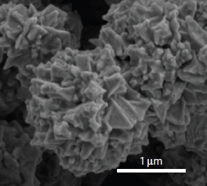
In SAC, tiny spheres of polyvinylidene fluoride (PVDF) encapsulate much of the liquid. The viscous polydimethylsiloxane (PDMS) further coats the entire surface. The spheres are extremely resilient, Lou said, as their thin shells deform easily. Their liquid contents enhance their viscoelasticity, a measure of their ability to absorb the strain and return to their original state, while the coatings keep the spheres together. The spheres also have the freedom to slide past each other when compressed, but remain attached.

Characterization of the hierarchical solid-liquid composite. (a) Image of solid-liquid SAC. (b) SEM image of the porous SAC. (c) High magnification SEM image of the shell of the bead. (credit: Pei Dong et al./ACS Appl. Mater. Interfaces)

“The sample doesn’t give you the impression that it contains any liquid,” he said. “That’s very different from a gel. This is not really squishy; it’s more like a sugar cube that you can compress quite a lot. The nice thing is that it recovers.”

Making SAC is simple, and the process can be tuned — a little more liquid or a little more solid — to regulate the product’s mechanical behavior. The polymer components begin as powder and viscous liquid. With the addition of a solvent and controlled heating, the PDMS stabilizes into solid spheres that provide the reconfigurable internal structure.

In tests, Rice scientists found a maximum of 683 percent increase in the material’s storage modulus — a size-independent parameter used to characterize self-stiffening behavior. This is much larger than that reported for solid composites and other materials, they said.


Rice University | Self-adaptive material heals itself, stays tough


Abstract of A Solid-liquid Self-adaptive Polymeric Composite

A solid-liquid self-adaptive composite (SAC) is synthesized using a simple mixing-evaporation protocol, with Poly(dimethylsiloxane) (PDMS) and Poly(vinylidene fluoride) (PVDF) as active constituents. SAC exists as a porous solid containing a near equivalent distribution of the solid (PVDF)-liquid (PDMS) phases, with the liquid encapsulated and stabilized within a continuous solid network percolating throughout the structure. The pores, liquid and solid phases form a complex hierarchical structure, which offers both mechanical robustness and a significant structural adaptability under external forces. SAC exhibits attractive self-healing properties during tension, and demonstrates reversible self-stiffening properties under compression with a maximum of seven-fold increase seen in the storage modulus. Compared to existing self-healing and self-stiffening materials, SAC offers distinct advantages in the ease of fabrication, high achievable storage modulus, and reversibility. Such materials could provide a new class of adaptive materials system with multi-functionality, tunability, and scale-up potentials.

A battery that shuts down at high temperatures and restarts when it cools

Stanford researchers have developed a thin polyethylene film that prevents a lithium-ion battery from overheating, then restarts the battery when it cools. The film is embedded with spiky nanoparticles of graphene-coated nickel. (credit: Zheng Chen)

Stanford researchers have invented a lithium-ion battery that shuts down before overheating to prevent the battery fires that have plagued laptops, hoverboards and other electronic devices. The battery restarts immediately when the temperature cools.

The design is an enhancement of a wearable sensor that monitors human body temperature invented by Zhenan Bao, a professor of chemical engineering at Stanford. The sensor is made of a plastic material embedded with tiny particles of nickel with nanoscale spikes protruding from their surface. For the battery experiment, the researchers coated the spiky nickel particles with graphene, an atom-thick layer of carbon, and embedded the particles in a thin film of elastic polyethylene.

SEM image of conductive spiky graphene-coated nickel nanoparticles (credit: Zheng Chen et al./Nature Energy)

To conduct electricity, the spiky particles have to physically touch one another. But during thermal expansion, polyethylene stretches. That causes the particles to spread apart, making the film non-conductive so that electricity can no longer flow through the battery. When the battery cools, the polyethylene shrinks, bringing the particles in contact again and causing the battery to generate power.

The new battery design has up to 10,000 times higher temperature sensitivity than previous switch devices, and the temperature range can be adjusted by changing the particle density or type of polymer.

“We’ve designed the first battery that can be shut down and revived over repeated heating and cooling cycles without compromising performance,” says Bao. The new battery is described in a study published today (Jan. 11) in the new journal Nature Energy.


Delvon Simmons | My hover board on fire

A typical lithium-ion battery today consists of two electrodes and a liquid or gel electrolyte that carries charged particles between them. Puncturing, shorting or overcharging the battery generates heat. If the temperature reaches about 300 degrees Fahrenheit (150 degrees Celsius), the electrolyte could catch fire and trigger an explosion, as some hoverboard users have recently discovered.

The research was supported by the SLAC National Accelerator Laboratory and the Precourt Institute for Energy at Stanford.

Stanford Precourt Institute for Energy | A lithium-ion battery that shuts down before overheating, then restarts immediately when the temperature cools.


Abstract of  Fast and reversible thermoresponsive polymer switching materials for safer batteries

Safety issues have been a long-standing obstacle impeding large-scale adoption of next-generation high-energy-density batteries. Materials solutions to battery safety management are limited by slow response times and small operating voltage windows. Here we report a fast and reversible thermoresponsive polymer switching material that can be incorporated inside batteries to prevent thermal runaway. This material consists of electrochemically stable graphene-coated spiky nickel nanoparticles mixed in a polymer matrix with a high thermal expansion coefficient. The as-fabricated polymer composite films show high electrical conductivity of up to 50 S per cm at room temperature. Importantly, the conductivity decreases within 1 s by seven to eight orders of magnitude on reaching the transition temperature and spontaneously recovers at room temperature. Batteries with this self-regulating material built in the electrode can rapidly shut down under abnormal conditions such as overheating and shorting, and are able to resume their normal function without performance compromise or detrimental thermal runaway. Our approach offers 1,000–10,000 times higher sensitivity towards temperature changes than previous switching devices.

Single-molecule detection of contaminants, explosives or diseases now possible

Artistic illustration showing an ultrasensitive detection platform termed “slippery liquid infused porous surface-enhanced Raman scattering” (SLIPSERS). An aqueous or oil droplet containing gold nanoparticles and captured analytes is allowed to evaporate on a slippery substrate, leading to the formation of a highly compact nanoparticle aggregate for use in surface-enhanced Raman scattering (SERS) detection. (credit: Shikuan Yang, Birgitt Boschitsch Stogin and Tak-Sing Wong/Penn State)

Penn State researchers have invented a way to detect single molecules of a number of chemical and biological species from gaseous, liquid or solid samples, with applications in analytical chemistry, molecular diagnostics, environmental monitoring and national security.

The invention is called SLIPSERS, an acronym combining “slippery liquid-infused porous surfaces” (SLIPS) and surface enhanced Raman scattering (SERS).*

“Being able to identify a single molecule is already very difficult. Being able to detect those molecules in all three phases [air, liquid, or bound to a solid] — that is really challenging,” said Tak-Sing Wong, assistant professor of mechanical engineering and the Wormley Family Early Career Professor in Engineering.

Although there are other techniques that allow researchers to concentrate molecules on a surface, those techniques mostly work with water as the medium. SLIPS can be used with any organic liquids, which makes it useful for environmental detection in soil samples, for example.

One of the researchers’ next steps will be to detect biomarkers in blood for disease diagnosis at very early stages of cancer when the disease is more easily treatable.

“Although the SLIPS technology is patented and licensed, the team has not sought patent protection on their SLIPSER work. “We believe that offering this technology to the public will get it developed at a much faster pace,” said Professor Wong. “This is a powerful platform that we think many people will benefit from.”

Their work appears an open-access online paper in Proceedings of the National Academy of Sciences (PNAS). It was funded by the National Science Foundation.

* Raman spectroscopy is a well-known method of analyzing materials in a liquid form using a laser to interact with the vibrating molecules in the sample, generating scattered light. But the molecule’s unique vibration shifts the frequency of the photons in the laser light beam up or down in a way that is characteristic of only that type of molecule, allowing it be uniquely identified.

However, the Raman signal is typically very weak and has to be enhanced in some way for detection. In the 1970s, researchers found that chemically roughening the surface of a silver substrate concentrated the Raman signal of the material adsorbed on the silver, and SERS was born.

Wong developed SLIPS as a post-doctoral researcher at Harvard University. SLIPS is composed of a surface coated with regular arrays of nanoscale posts infused with a liquid lubricant that does not mix with other liquids. The small spacing of the nanoposts traps the liquid between the posts and the result is a slippery surface that nothing adheres to.

“The problem,” Wong said, “is that trying to find a few molecules in a liquid medium is like trying to find a needle in a haystack. But if we can develop a process to gradually shrink the size of this liquid volume, we can get a better signal. To do that we need a surface that allows the liquid to evaporate uniformly until it gets to the micro or nanoscale. Other surfaces can’t do that, and that is where SLIPS comes in.”

The researchers assemble the gold nanoparticles so they have nanoscale gaps, called SERS “hot spots.” Using a laser with the right wavelength, the electrons will oscillate and a strong magnetic field will form in the gap area. This gives us very strong SERS signals of the molecules located within the gaps.”

If a droplet of liquid is placed on any normal surface, it will begin to shrink from the top down. When the liquid evaporates, the target molecules are left in random configurations with weak signals. But if all the molecules can be clustered among the gold nanoparticles, they will produce a very strong Raman signal.


Abstract of Ultrasensitive surface-enhanced Raman scattering detection in common fluids

Many analytes in real-life samples, such as body fluids, soil contaminants, and explosives, are dispersed in liquid, solid, or air phases. However, it remains a challenge to create a platform to detect these analytes in all of these phases with high sensitivity and specificity. Here, we demonstrate a universal platform termed slippery liquid-infused porous surface-enhanced Raman scattering (SLIPSERS) that enables the enrichment and delivery of analytes originating from various phases into surface-enhanced Raman scattering (SERS)-sensitive sites and their subsequent detection down to the subfemtomolar level (<10−15 mol⋅L−1). Based on SLIPSERS, we have demonstrated detection of various chemicals, biological molecules, and environmental contaminants with high sensitivity and specificity. Our platform may lead to ultrasensitive molecular detection for applications related to analytical chemistry, diagnostics, environmental monitoring, and national security.

Algorithm turns smartphones into 3-D scanners

Structured light 3-D scanning normally requires a projector and camera to be synchronized. A new technique eliminates the need for synchronization, which makes it possible to do structured light scanning with a smartphone. (credit: Taubin Lab/Brown University)

An algorithm developed by Brown University researchers my help bring high-quality 3-D depth-scanning capability to standard commercial digital cameras and smartphones.

“The 3-D scanners on the market today are either very expensive or unable to do high-resolution image capture, so they can’t be used for applications where details are important,” said Gabriel Taubin, a professor in Brown’s School of Engineering — like 3-D printing.

Most of the high-quality 3-D scanners capture images using a technique known as structured light. A projector casts a series of light patterns on an object, while a camera captures images of the object. The way these patterns deform when striking surfaces allows the structured-light 3-D scanner to calculate the depth and surface configurations of the objects in the scene, creating a 3-D image.

No sync required

The limitation with current 3-D depth scanners is that the pattern projector and the camera have to precisely synchronized, which requires specialized and expensive hardware.

The problem in trying to capture 3-D images without synchronization is that the projector could switch from one pattern to the next while the image is in the process of being exposed. As a result, the captured images are mixtures of two or more patterns. A second problem is that most modern digital cameras use a rolling shutter mechanism. Rather than capturing the whole image in one snapshot, cameras scan the field either vertically or horizontally, sending the image to the camera’s memory one pixel row at a time. As a result, parts of the image are captured a slightly different times, which also can lead to mixed patterns.

The fix

The algorithm Taubin and his students have developed enables the structured light technique to be done without synchronization between projector and camera. That means an off-the-shelf camera can be used with an untethered (unconnected by a wire) structured light flash. The camera just needs to have the ability to capture uncompressed images in burst mode (several successive frames per second), which many DSLR cameras and smartphones can do.

After the camera captures a burst of images, the algorithm calibrates the timing of the image sequence using the binary information embedded in the projected pattern. Then it goes through the images, pixel by pixel, to assemble a new sequence of images that captures each pattern in its entirety. Once the complete pattern images are assembled, a standard structured light 3D reconstruction algorithm can be used to create a single 3-D image of the object or space.

The researchers presented a paper describing the algorithm last month at the SIGGRAPH Asia computer graphics conference. In their paper, the researchers showed that the technique works just as well as synchronized structured light systems. During testing, the researchers used a fairly standard structured light projector, but the team envisions working to develop a structured light flash that could eventually be used as an attachment to any camera.

Northwestern University engineers have developed another inexpensive solution to the problem (see A fast, high-quality, inexpensive 3-D camera), but it uses a proprietary 3-D capture camera instead of an existing smartphone.


Abstract of Unsynchronized structured light

Various Structured Light (SL) methods are used to capture 3D range images, where a number of binary or continuous light patterns are sequentially projected onto a scene of interest, while a digital camera captures images of the illuminated scene. All existing SL methods require the projector and camera to be hardware or software synchronized, with one image captured per projected pattern. A 3D range image is computed from the captured images. The two synchronization methods have disadvantages, which limit the use of SL methods to niche industrial and low quality consumer applications. Unsynchronized Structured Light (USL) is a novel SL method which does not require synchronization of pattern projection and image capture. The light patterns are projected and the images are captured independently, at constant, but possibly different, frame rates. USL synthesizes new binary images as would be decoded from the images captured by a camera synchronized to the projector, reducing the subsequent computation to standard SL. USL works both with global and rolling shutter cameras. USL enables most burst-mode-capable cameras, such as modern smartphones, tablets, DSLRs, and point-and-shoots, to function as high quality 3D snapshot cameras. Beyond the software, which can run in the devices, a separate SL Flash, able to project the sequence of patterns cyclically, during the acquisition time, is needed to enable the functionality.

MIT uses forests of carbon nanotubes with antibodies to capture hard-to-detect molecules

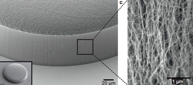
Scanning electron microscope image of carbon nanotubes showing textured porosity (credit: Allison L. Yost et al./Microsystems & Nanoengineering)

Engineers at MIT have devised a new technique for trapping hard-to-detect molecules, using forests of coated carbon nanotubes.

The team modified a simple microfluidic channel with an array of vertically aligned carbon nanotubes — rolled lattices of carbon atoms that resemble tiny tubes of chicken wire.

Carbon-nanotube posts can trap cancer and other cells as they flow through a microfluidic device (credit: Brian Wardle)

The researchers had previously devised a method for standing carbon nanotubes on their ends, like trees in a forest (see “Trapping cancer cells with carbon nanotubes“). This 3-D array of permeable carbon nanotubes allows fluid to flow through a microfluidic device.

Now, in a study published this week in the Journal of Microengineering and Nanotechnology, the researchers have given the nanotube array the additional ability to trap specific particles. To do this, the team coated the array, layer by layer, with polymers of alternating electric charge.

Depending on the number of layers deposited, the researchers can create thicker or thinner nanotubes and thereby tailor the porosity of the forest to capture larger or smaller particles of interest. The nanotubes’ polymer coating can also be chemically manipulated to bind specific bioparticles flowing through the forest.

The combination of carbon nanotubes and multilayer coatings may help finely tune microfluidic devices to capture extremely small and rare particles, such as certain viruses and proteins, says Brian Wardle, professor of aeronautics and astronautics at MIT.

“There are smaller bioparticles that contain very rich amounts of information that we don’t currently have the ability to access in point-of-care [medical testing] devices like microfluidic chips,” says Wardle, who is a co-author on the paper. “Carbon nanotube arrays could actually be a platform that could target that size of bioparticle.”

What’s more, Wardle says, a three-dimensional forest of carbon nanotubes would provide much more surface area on which target molecules may interact, compared with the two-dimensional surfaces in conventional microfluidics.

Capturing specific particles of interest

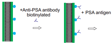
To test this idea, the researchers used an established technique to treat the surface of the nanotubes with antibodies that bind to prostate specific antigen (PSA), a common experimental target.

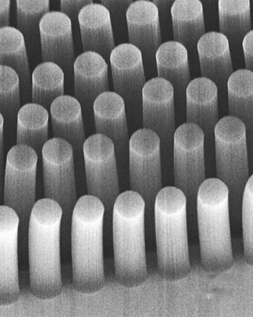
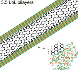
A 3-D array of carbon nanotubes on a microfluidic device coated with successive layers of alternately charged polymer solutions (credit: Allison L. Yost et al./Microsystems & Nanoengineering)

The team integrated a 3-D array of carbon nanotubes into a microfluidic device by using chemical vapor deposition and photolithography to grow and pattern carbon nanotubes onto silicon wafers. They then grouped the nanotubes into a cylinder-shaped forest, measuring about 50 micrometers tall and 1 millimeter wide, and centered the array within a 3 millimeter-wide, 7-millimeter long microfluidic channel.

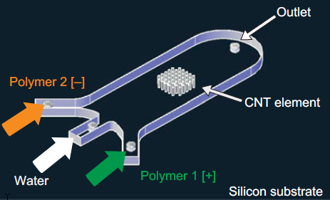
Polyelectrolyte multilayer (PEM) film deposition on carbon-nanotube surface (credit: Allison L. Yost et al./Microsystems & Nanoengineering)

The researchers coated the nanotubes in successive layers of alternately charged polymer solutions to create distinct, binding layers around each nanotube. To do so, they flowed each solution through the channel and found they were able to create a more uniform coating with a gap between the top of the nanotube forest and the roof of the channel. Such a gap allowed solutions to flow over, then down into the forest, coating each individual nanotube.

Carbon nanotube treated with antibodies for PSA capture (credit: Allison L. Yost et al./Microsystems & Nanoengineering)

After coating the nanotube array in layers of polymer solution, the researchers demonstrated that the array could be primed to detect a given molecule by treating it with antibodies that typically bind to prostate specific antigen (PSA). They pumped in a solution containing small amounts of PSA and found that the array captured the antigen effectively, throughout the forest, rather than just on the outer surface of a typical microfluidic element.

The polymer-coated arrays captured 40 percent more antigens, compared with arrays lacking the polymer coating.

Wardle says that the nanotube array is extremely versatile. The carbon nanotubes can be manipulated mechanically, electrically, and optically and the polymer coatings can be chemically altered to capture a wide range of particles. He says an immediate target may be biomarkers called exosomes, which are less than 100 nanometers wide and can be important signals of a disease’s progression.

“This type of device actually has all the characteristics and functionality that would allow you to go after bioparticles like exosomes and things that really truly are nanometer scale,” he noted.

This research was funded in part by the National Science Foundation.


Abstract of Layer-by-layer functionalized nanotube arrays: A versatile microfluidic platform for biodetection

We demonstrate the layer-by-layer (LbL) assembly of polyelectrolyte multilayers (PEM) on three-dimensional nanofiber scaffolds. High porosity (99%) aligned carbon nanotube (CNT) arrays are photolithographically patterned into elements that act as textured scaffolds for the creation of functionally coated (nano)porous materials. Nanometer-scale bilayers of poly(allylamine hydrochloride)/poly(styrene sulfonate) (PAH/SPS) are formed conformally on the individual nanotubes by repeated deposition from aqueous solution in microfluidic channels. Computational and experimental results show that the LbL deposition is dominated by the diffusive transport of the polymeric constituents, and we use this understanding to demonstrate spatial tailoring on the patterned nanoporous elements. A proof-of-principle application, microfluidic bioparticle capture using N-hydroxysuccinimide-biotin binding for the isolation of prostate-specific antigen (PSA), is demonstrated.

Magnetic nanoparticles combat biofilms, a source of chronic bacterial infections

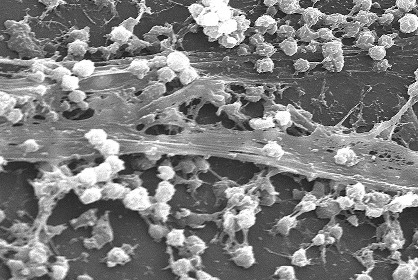
Staphylococcus aureus bacterial biofilm on an indwelling catheter (credit: CDC)

A solution for biofilms* — a scourge of infections in hospitals and kitchens formed by bacteria that stick to each other on living tissue and medical instruments — has been developed by University of New South Wales researchers: Injecting iron oxide nanoparticles into the biofilms, and using an applied magnetic field to heat them, triggering them into dispersing.

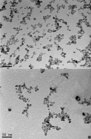
Transmission electron microscopy (TEM) micrographs of dried nanoparticles before (top) and after (bottom) conjugation with polymer (credit: Thuy-Khanh Nguyen et al./Scientific Reports)

“Chronic biofilm-based infections are often extremely resistant to antibiotics and many other conventional antimicrobial agents, and have a high capacity to evade the body’s immune system,” said Associate Professor Cyrille Boyer of the School of Chemical Engineering and deputy director of Australian Centre for NanoMedicine. “Our study points to a pathway for the non-toxic dispersal of biofilms in infected tissue, while also greatly improving the effect of antibiotic therapies.”

When biofilms want to colonize a new site, they disperse into individual cells, reducing the protective action of the biofilm. It is this process the UNSW team sought to trigger. They achieved this using iron oxide nanoparticles coated with polymers that help stabilize and maintain the nanoparticles in a dispersed state, making them an ideal non-toxic tool for treating biofilm infection.

Once dispersed, the bacteria are easier to deal with, creating the potential to remove recalcitrant, antimicrobial-tolerant biofilm infections with antimicrobial agents.

The discovery of how to dislodge biofilms by the UNSW Faculty of Engineering team was made using the opportunistic human pathogen Pseudomonas aeruginosa. This is a model organism whose response to the technique the researchers believe will apply to most other bacteria.

“The use of these polymer-coated iron oxide nanoparticles to disperse biofilms may have broad applications across a range of clinical and industrial settings,” said Boyer.

The research appears in an open-access paper today (Dec. 21) in Nature’s Scientific Reports.

* Biofilms have been linked to 80% of infections, forming on living tissues (e.g. respiratory, gastrointestinal and urinary tracts, oral cavities, eyes, ears, wounds, heart and cervix) or dwelling in medical devices (e.g. dialysis catheters, prosthetic implants and contact lenses).

The formation of biofilms is a growing and costly problem in hospitals, creating infections that are more difficult to treat — leading to chronic inflammation, impaired wound healing, rapidly acquired antibiotic resistance and the spread of infectious embolisms in the bloodstream.

They also cause fouling and corrosion of wet surfaces, and the clogging of filtration membranes in sensitive equipment, even posing a threat to public health by acting as reservoirs of pathogens in distribution systems for drinking water.

In general, bacteria have two life forms during growth and proliferation: planktonic, where bacteria exist as single, independent cells; or aggregated together in colonies as biofilms, where bacteria grow in a slime-like polymer matrix that protects them from the environment around them.

Acute infections mostly involve planktonic bacteria, which are usually treatable with antibiotics. However, when bacteria have had enough time to form a biofilm — within a human host or non-living material such as dialysis catheters – an infection can often become untreatable and develop into a chronic state.


UNSW | 2015 Malcolm McIntosh Prize for Physical Scientist of the Year


Abstract of Iron oxide nanoparticle-mediated hyperthermia stimulates dispersal in bacterial biofilms and enhances antibiotic efficacy

The dispersal phase that completes the biofilm lifecycle is of particular interest for its potential to remove recalcitrant, antimicrobial tolerant biofilm infections. Here we found that temperature is a cue for biofilm dispersal and a rise by 5 °C or more can induce the detachment of Pseudomonas aeruginosa biofilms. Temperature upshifts were found to decrease biofilm biomass and increase the number of viable freely suspended cells. The dispersal response appeared to involve the secondary messenger cyclic di-GMP, which is central to a genetic network governing motile to sessile transitions in bacteria. Furthermore, we used poly((oligo(ethylene glycol) methyl ether acrylate)-block-poly(monoacryloxy ethyl phosphate)-stabilized iron oxide nanoparticles (POEGA-b-PMAEP@IONPs) to induce local hyperthermia in established biofilms upon exposure to a magnetic field. POEGA-b-PMAEP@IONPs were non-toxic to bacteria and when heated induced the detachment of biofilm cells. Finally, combined treatments of POEGA-b-PMAEP@IONPs and the antibiotic gentamicin reduced by 2-log the number of colony-forming units in both biofilm and planktonic phases after 20 min, which represent a 3.2- and 4.1-fold increase in the efficacy against planktonic and biofilm cells, respectively, compared to gentamicin alone. The use of iron oxide nanoparticles to disperse biofilms may find broad applications across a range of clinical and industrial settings.

Mystery material stuns scientists

How does water on the surface of this bizarre material control UV light emission and also its conductivity? (credit: Mohammad A. Islam et al./Nano Letters)

In a remarkable chance landmark discovery, a team of researchers at four universities has discovered a mysterious material that emits ultraviolet light and has insulating, electrical conducting, semiconducting, superconducting, and ferromagnetic properties — all controlled by surface water.

It happened while the researchers were studying a sample of lanthanum aluminate film on a strontinum titanate crystal. The sample mysteriously began to glow, emitting intense levels of ultraviolet light from its interior. After carefully reproducing the experimental conditions, they tracked down the unlikely switch that turns UV light on or off: surface water moisture.

The team of researchers from Drexel University, the University of Pennsylvania, the University of California at Berkeley, and Temple University also found that the interface between the materials’ two layers of electrical insulators also had an unusual electrical conducting state that, like UV, could also be altered by the water on the surface. On top of that, the material also exhibited superconducting, ferromagnetic ordering, and photoconductive properties.

Even weirder, “we can also make [the effects] stronger by increasing the distance between the molecules and surface and the buried interface, by using thicker films for example,” said Drexel College of Engineering Professor Jonathan E. Spanier.

Calling in the theorists

Puzzled, the researchers turned to their theory collaborators on the team: Penn’s Andrew M. Rappe, Fenggong Wang, and Diomedes Saldana-Grego.

“Dissociation of water fragments on the oxide surface releases electrons that move to the buried interface, cancelling out the ionic charges,” Wang said. “This puts all the light emission at the same energy, giving the observed sharp photoluminescence.”

According to Rappe, this is the first report of the introduction of molecules to the surface controlling the emission of light — of any color — from a buried solid-surface interface. “The mechanism of a molecule landing and reacting, called dissociative chemisorption, as a way of controlling the onset and suppression of light is unlike any other previously reported,” Saldana-Grego added.

The team recently published its findings in the American Chemical Society journal Nano Letters.

Multiple personality

“We suspect that the material could be used for simple devices like transistors and [chemical] sensors,” said Mohammad Islam, an assistant professor from the State University of New York at Oswego, who was on Spanier’s team when he was at Drexel.

“By strategically placing molecules on the surface, the UV light could be used to relay information — much the way computer memory uses a magnetic field to write and rewrite itself, but with the significant advantage of doing it without an electric current. The strength of the UV field also varies with the proximity of the water molecule; this suggests that the material could also be useful for detecting the presence of chemical agents.”


Abstract of Surface Chemically Switchable Ultraviolet Luminescence from Interfacial Two-Dimensional Electron Gas

We report intense, narrow line-width, surface chemisorption-activated and reversible ultraviolet (UV) photoluminescence from radiative recombination of the two-dimensional electron gas (2DEG) with photoexcited holes at LaAlO3/SrTiO3. The switchable luminescence arises from an electron transfer-driven modification of the electronic structure via H-chemisorption onto the AlO2-terminated surface of LaAlO3, at least 2 nm away from the interface. The control of the onset of emission and its intensity are functionalities that go beyond the luminescence of compound semiconductor quantum wells. Connections between reversible chemisorption, fast electron transfer, and quantum-well luminescence suggest a new model for surface chemically reconfigurable solid-state UV optoelectronics and molecular sensing.

A color laser printer with an amazing 127,000 dots per inch resolution

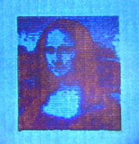
A laser-printed microscopic image of Mona Lisa 50 micrometers long, less than one pixel on an iPhone Retina display (credit: Technical University of Denmark)

A new laser-printing technology allows for printing high-resolution data and color images at the unprecedented resolution of 127,000 dots per inch (DPI) and with a speed of 1 nanosecond per pixel — developed by researchers at Technical University of Denmark’s DTU Nanotech and DTU Fotonik.

At that extreme resolution, images can be printed on the microscale. This patented method uses special plasmonic metasurfaces coated with 20 nanometers of aluminum. When a laser pulse heats each nanocolumn (up to 1,500°C for a few nanoseconds), it melts and is deformed.

The intensity of the laser beam heating controls the amount of deformation, which determines which color are printed. Low-intensity laser pulses lead to a minor deformation of the nanocolumn, resulting in blue and purple hue reflections. Stronger laser pulses create a larger deformation, which  leads to reflection from the nanocolumn at longer wavelength orange and yellow hue.

According to Professor Anders Kristensen, it’s also possible to save data invisible to the naked eye with this technology. “This includes serial numbers or bar codes of products and other information. The technology can also be used to combat fraud and forgery, as the products will be labeled in way that makes them very difficult to reproduce. It will be easier to determine whether the product is an original or a copy.”

The new laser printing technology can also be used on a larger scale to personalize products such as mobile phones with unique decorations, names, etc. and for  marking parts for cars, such as instrument panels and buttons. The scientists hope to eventually replace conventional laser printers.


Abstract of Plasmonic colour laser printing

Colour generation by plasmonic nanostructures and metasurfaces has several advantages over dye technology: reduced pixel area, sub-wavelength resolution and the production of bright and non-fading colours. However, plasmonic colour patterns need to be pre-designed and printed either by e-beam lithography (EBL) or focused ion beam (FIB), both expensive and not scalable processes that are not suitable for post-processing customization. Here we show a method of colour printing on nanoimprinted plasmonic metasurfaces using laser post-writing. Laser pulses induce transient local heat generation that leads to melting and reshaping of the imprinted nanostructures. Depending on the laser pulse energy density, different surface morphologies that support different plasmonic resonances leading to different colour appearances can be created. Using this technique we can print all primary colours with a speed of 1 ns per pixel, resolution up to 127,000 dots per inch (DPI) and power consumption down to 0.3 nJ per pixel.

When wearable electronics devices disappear into clothes

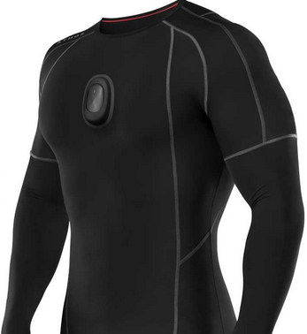
The Athos Upper Body Package includes 14 built in sensors for real-time muscle and heart rate data. (credit: Athos)

Wearables will “disappear” in 2016, predicts New Enterprise Associates venture capital partner Rick Yang, cited in a Wednesday (Dec. 16) CNBC article — integrated “very directly into your everyday life, into your existing fashion sense to the extent that nobody knows you’re wearing a wearable,” he said.

For example, Athos makes smart workout clothes embedded with inconspicuous technology that tracks muscle groups, heart, and breathing rates, he noted.

But taking that next step in wearable technology means ditching bulky, clothes-deforming batteries. Supercapacitors (see “Flexible 3D graphene supercapacitors may power portables and wearables“), as discussed on KurzweilAI, are a perfect match for that. They work like tiny batteries, but unlike batteries, they can be rapidly charged and deliver more power quickly in a smaller space.

They’re a lot smaller and thinner than batteries. But still too bulky.

Weaving electronics into fabrics

Enter Case Western Reserve University researchers, who announced Wednesday that have developed flexible wire-shaped microsupercapacitors that can be embedded as microscopic-sized wires directly in fabrics. These provide three times higher capacitance than previous attempts to create microsupercapacitors, the researchers say.*

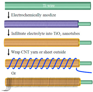
Wearable wires (credit: Tao Chen, Liming Dai/Energy Storage Materials)

In this new design, the modified titanium wire is coated with a solid electrolyte made of polyvinyl alcohol and phosphoric acid. The wire is then wrapped with either yarn or a sheet made of aligned carbon nanotubes, which serves as the second electrode.

The titanium oxide nanotubes, which are semiconducting, separate the two active portions of the electrodes, preventing a short circuit.

“They’re very flexible, so they can be integrated into fabric or textile materials,” said Liming Dai, the Kent Hale Smith Professor of Macromolecular Science and Engineering. “They can be a wearable, flexible power source for wearable electronics and also for self-powered biosensors or other biomedical devices, particularly for applications inside the body.”

The scientists published their research on the microsupercapacitor in the journal Energy Storage Materials this week. The study builds on earlier carbon-based supercapacitors.

Conductive inks

An article just published in Chemical & Engineering News (C&EN) profiles textiles printed with such stretchable embedded wiring and electronic sensors, which can transmit data wirelessly and withstand washing.

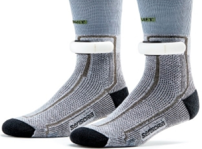
Smart socks (credit: Sensoria)

For example, “smart socks” incorporate stretchable silver-based conductive yarns that connect their sensors to a magnetic Bluetooth electronic anklet that transmits data to a mobile app to keep track of foot landings, cadence, and time on the ground.

The data are intended to help runners improve their form and performance. Two pairs of socks and an anklet cost $200.

C&EN also highlights another key technology: conductive inks, which are used by BeBop Sensors in a design for a thin shoe insole integrated with piezoresistive-fabric sensors and silicon-based electronics, which are capable of measuring a wearer’s foot pressure.

They’ve also developed a conceptual design for a car steering wheel cover that senses driver alertness and weight-lifting gloves that sense weight and load distribution between hands.

Mounir Zok, senior sports technologist for the U.S. Olympic Committee dates the beginning of wearable technology to 2002, when relatively small electronic devices first began to replace the probes, electrodes, and masks that athletes wore while tethered to monitoring equipment in training labs, C&EN notes.

Devices to measure heart rate, power, cadence, and speed can lead to improved performance for athletes, Zok explained. Many of the first wearable devices designed for track and field were cumbersome and interfered with performance. But the smaller, more flexible, less power-hungry devices available today are helping Zok and his colleagues better monitor athletic improvements.

* In a lab experiment, the microsupercapactitor was able to store 1.84 milliFarads per micrometer. Energy density was 0.16 x 10⁻³ milliwatt-hours per cubic centimeter and power density .01 milliwatt per cubic centimeter.


Abstract of Flexible and wearable wire-shaped microsupercapacitors based on highly aligned titania and carbon nanotubes

Wire-shaped devices, such as solar cells and supercapacitors, have attracted great attentions due to their unique structure and promise to be integrated into textiles as portable energy source. To date, most reported wire-shaped supercapacitors were developed based on carbon nanomaterial-derived fiber electrodes whereas titania was much less used, though with excellent pseudocapacitvie properties. In this work, we used a titanium wire sheathed with radially aligned titania nanotubes as one of the electrodes to construct all-solid-state microsupercapacitors, in which the second electrode was carbon nanotube fiber or sheet. The capacitance of the resulting microsupercapacitor with a CNT sheet electrode (1.84 mF cm−2) is about three time of that for the corresponding device with the second electrode based on a single CNT yarn. The unique wire-shaped structure makes it possible for the wire-shaped microsupercapacitors to be woven into various textiles and connected in series or parallel to meet a large variety of specific energy demands.

New nanomanufacturing technique for extremely high-resolution imaging, biological sensing

Schematic of the fabrication process and SEM images of the nanostructures used to create a nanolens. (credit: Augustine Urbas et al./Advanced Materials)

Researchers have developed a method of constructing nanolenses that could focus incoming light into a spot much smaller than possible with conventional microscopy, making possible extremely high-resolution imaging or biological sensing.

They precisely aligned three spherical gold nanoparticles of graduated sizes in a string-of-pearls arrangement  to produce the focusing effect.

The first step employs the lithographic methods used in making printed circuits to create a chemical mask that leaves a pattern of three spots of decreasing size exposed on a substrate such as silicon or glass that won’t absorb the gold nanoparticles. Lithography allows for extremely precise and delicate patterns, but it can’t produce three-dimensional structures. So the scientists used chemistry to build polymer chains atop the patterned substrate in three dimensions, tethered to the substrate through chemical bonds.

“The chemical contrast between the three spots and the background makes the gold particles go only to the spots,” said Xiaoying Liu, senior research scientist at the University of Chicago’s Institute for Molecular Engineering. To get each of the three sizes of nanospheres to adhere only to its own designated spot, the scientists played with the strength of the chemical interaction between spot and sphere. “We control the size of the different areas in the chemical pattern and we control the interaction potential of the chemistry of those areas with the nanoparticles,” said Nealey.

The spheres are separated by only a few nanometers. It is this tiny separation, coupled with the sequential ordering of the different-sized spheres, that produces the nanolensing effect.

High-resolution sensing using spectroscopy

The scientists are already exploring using this “hot spot” for high-resolution sensing using spectroscopy. “If you put a molecule there, it will interact with the focused light,” said Liu. “The enhanced field at these hot spots will help you to get orders of magnitude stronger signals. And that gives us the opportunity to get ultra-sensitive sensing. Maybe ultimately we can detect single molecules.”

The researchers also foresee applying their manufacturing technique to nanoparticles of other shapes, such as rods and stars.

Scientists at the Air Force Research Laboratory and Florida State University were also involved in the research, which is described in the latest edition of Advanced Materials.


Abstract of Deterministic Construction of Plasmonic Heterostructures in Well-Organized Arrays for Nanophotonic Materials

Plasmonic heterostructures are deterministically constructed in organized arrays through chemical pattern directed assembly, a combination of top-down lithography and bottom-up assembly, and by the sequential immobilization of gold nanoparticles of three different sizes onto chemically patterned surfaces using tailored interaction potentials. These spatially addressable plasmonic chain nanostructures demonstrate localization of linear and nonlinear optical fields as well as nonlinear circular dichroism.