‘Porous liquid’ invention could lead to improved carbon capture

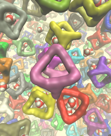
World’s first “porous liquid” (credit: Queen’s University Belfast)

Scientists at Queen’s University Belfast, Northern Ireland, and partners have invented a “porous liquid” that can dissolve unusually large amounts of gas, with the potential for a wide range of new uses, including carbon capture.

They designed the new liquid from the bottom up, designing the shapes of the “cage molecules” to form empty holes. The researchers say the concentration of unoccupied cages can be around 500 times greater than in other molecular solutions that contain cavities, enabling an eightfold increase in the solubility of methane gas, for example.

The results of their research were published Nov. 12 in the journal Nature.


Abstract of Liquids with permanent porosity

Porous solids such as zeolites and metal–organic frameworks are useful in molecular separation and in catalysis, but their solid nature can impose limitations. For example, liquid solvents, rather than porous solids, are the most mature technology for post-combustion capture of carbon dioxide because liquid circulation systems are more easily retrofitted to existing plants. Solid porous adsorbents offer major benefits, such as lower energy penalties in adsorption–desorption cycles, but they are difficult to implement in conventional flow processes. Materials that combine the properties of fluidity and permanent porosity could therefore offer technological advantages, but permanent porosity is not associated with conventional liquids5. Here we report free-flowing liquids whose bulk properties are determined by their permanent porosity. To achieve this, we designed cage molecules that provide a well-defined pore space and that are highly soluble in solvents whose molecules are too large to enter the pores. The concentration of unoccupied cages can thus be around 500 times greater than in other molecular solutions that contain cavities, resulting in a marked change in bulk properties, such as an eightfold increase in the solubility of methane gas. Our results provide the basis for development of a new class of functional porous materials for chemical processes, and we present a one-step, multigram scale-up route for highly soluble ‘scrambled’ porous cages prepared from a mixture of commercially available reagents. The unifying design principle for these materials is the avoidance of functional groups that can penetrate into the molecular cage cavities.

Multi-layer nanoparticles glow when exposed to invisible near-infrared light

An artist’s rendering shows the layers of a new, onion-like nanoparticle whose specially crafted layers enable it to efficiently convert invisible near-infrared light to higher-energy blue and UV light (credit: Kaiheng Wei)

A new onion-like nanoparticle developed at the State University of New York University at Buffalo could open new frontiers in biomaging, solar-energy harvesting, and light-based security techniques.

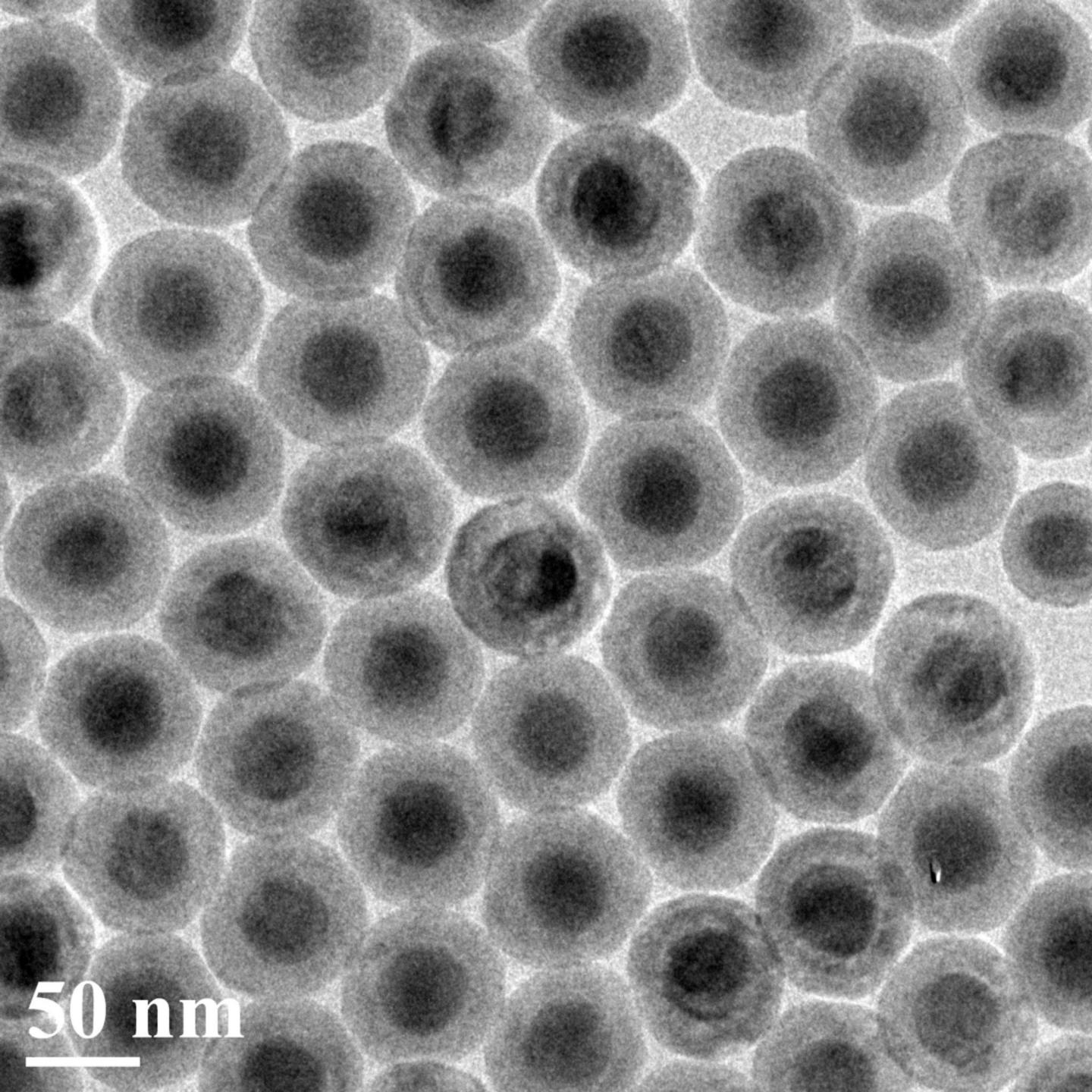
The particle’s innovation lies in its layers: a coating of organic dye, a neodymium-containing shell, and a core that incorporates ytterbium and thulium. Together, these strata convert invisible near-infrared light to higher energy blue and UV light with record-high efficiency.

A transmission electron microscopy image of the new nanoparticles, which convert invisible near-infrared light to higher-energy blue and UV light with high efficiency. Each particle is about 50 nanometers in diameter. (credit: Institute for Lasers, Photonics and Biophotonics, University at Buffalo)

Light-emitting nanoparticles placed by a surgeon inside the body could provide high-contrast images of areas of interest. Nanoparticle-infused inks could also be incorporated into currency designs using ink that is invisible to the naked eye but glows blue when hit by a low-energy near-infrared laser pulse — which would very difficult for counterfeiters to reproduce.

The researchers say the nanoparticle is about 100 times more efficient at “upconverting” [increasing the frequency of] light than similar nanoparticles.

Peeling back the layers

Energy-cascaded upconversion (credit: Guanying Chen et al./Nano Letters)

Converting low-energy light to light of higher energies is difficult to do. It involves capturing two or photons from a low-energy light source, and combining their energy to form a single, higher-energy photon. Each of the three layers of this onionesque nanoparticle fulfills a unique function:

  • The outermost layer is a coating of organic dye. This dye is adept at absorbing photons from low-energy near-infrared light sources. It acts as an “antenna” for the nanoparticle, harvesting light and transferring energy inside, Ohulchanskyy says.
  • The next layer is a neodymium-containing shell. This layer acts as a bridge, transferring energy from the dye to the particle’s light-emitting core.*
  • Inside the light-emitting core, ytterbium and thulium ions work in concert. The ytterbium ions draw energy into the core and pass the energy on to the thulium ions, which have special properties that enable them to absorb the energy of three, four or five photons at once, and then emit a single higher-energy photon of blue and UV light.

The research was published online in Nano Letters on Oct. 21. It was led by the Institute for Lasers, Photonics, and Biophotonics at UB, and the Harbin Institute of Technology in China, with contributions from the Royal Institute of Technology in Sweden, Tomsk State University in Russia, and the University of Massachusetts Medical School.

* The neodymium-containing layer is necessary for transferring energy efficiently from dye to core. When molecules or ions in a material absorb a photon, they enter an “excited” state from which they can transfer energy to other molecules or ions. The most efficient transfer occurs between molecules or ions whose excited states require a similar amount of energy to obtain, but the dye and ytterbium ions have excited states with very different energies. So the team added neodymium — whose excited state is in between that of the dye and thulium’s — to act as a bridge between the two, creating a “staircase” for the energy to travel down to reach emitting thulium ions.


Abstract of Energy-Cascaded Upconversion in an Organic Dye-Sensitized Core/Shell Fluoride Nanocrystal

Lanthanide-doped upconversion nanoparticles hold promises for bioimaging, solar cells, and volumetric displays. However, their emission brightness and excitation wavelength range are limited by the weak and narrowband absorption of lanthanide ions. Here, we introduce a concept of multistep cascade energy transfer, from broadly infrared-harvesting organic dyes to sensitizer ions in the shell of an epitaxially designed core/shell inorganic nanostructure, with a sequential nonradiative energy transfer to upconverting ion pairs in the core. We show that this concept, when implemented in a core–shell architecture with suppressed surface-related luminescence quenching, yields multiphoton (three-, four-, and five-photon) upconversion quantum efficiency as high as 19% (upconversion energy conversion efficiency of 9.3%, upconversion quantum yield of 4.8%), which is about ∼100 times higher than typically reported efficiency of upconversion at 800 nm in lanthanide-based nanostructures, along with a broad spectral range (over 150 nm) of infrared excitation and a large absorption cross-section of 1.47 × 10⁻¹⁴ cm2 per single nanoparticle. These features enable unprecedented three-photon upconversion (visible by naked eye as blue light) of an incoherent infrared light excitation with a power density comparable to that of solar irradiation at the Earth surface, having implications for broad applications of these organic–inorganic core/shell nanostructures with energy-cascaded upconversion.

New technology senses colors in the infrared spectrum

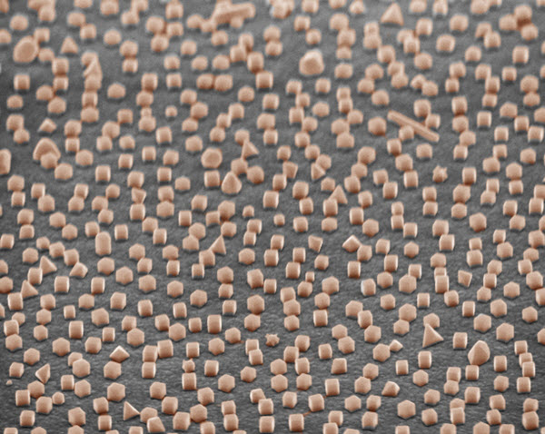
A scanning electron microscope image showing a surface coated with silver nanocubes on a gold surface to image near-infrared light (credit: Maiken Mikkelsen and Gleb Akselrod, Duke University)

Duke University scientists have invented a technology that can identify and image different wavelengths of the infrared spectrum.

The fabrication technique for the system is easily scalable, can be applied to any surface geometry, and costs much less than current light-absorption technologies, according to the researchers. Once adopted, the technique would allow advanced infrared imaging systems to be produced faster and cheaper than today’s counterparts and with higher sensitivity.

The visible-light spectrum, with wavelengths of about 400 to 700 nanometers. The near-infrared region starts just above the red region. (credit: Wikipedia)

Using nanoparticles to absorb specific wavelengths

The technology relies on a physics phenomenon called plasmonics to absorb or reflect specific wavelengths, similar to how stained-glass windows are created (see “Crafting color coatings from nanometer-thick layers of gold and germanium“).

A curved object covered with a coating of 100-nanometer silver cubes that absorbs all red light, leaving the object with a green tint (credit: Maiken Mikkelsen and Gleb Akselrod, Duke University)

The researchers first coat a surface with a thin film of gold through a common process like evaporation. They then put down a few-nanometer-thin layer of polymer, followed by a coating of silver cubes, each one about 100 nanometers (billionths of a meter) in size.

When light strikes the new engineered surface, a specific color gets trapped on the surface of the nanocubes in packets of energy called plasmons, and eventually dissipates into heat. By controlling the thickness of the polymer film and the size and number of silver nanocubes, the coating can be tuned to absorb different wavelengths of light from the visible spectrum (at 650 nm) to the near infrared (up to 1420 nm).

“By borrowing well-known techniques from chemistry and employing them in new ways, we were able to obtain significantly better resolution than with a million-dollar state-of-the-art electron beam lithography system,” said Maiken H. Mikkelsen, the Nortel Networks Assistant Professor of Electrical & Computer Engineering and Physics at Duke University. “This allowed us to create a coating that can fine-tune the absorption spectra with a level of control that hasn’t been possible previously.”

Coating photodetectors to absorb specific wavelengths of near-infrared light would allow novel and cheap cameras to be made that could capture and discriminate different wavelengths.

A better “tricorder” camera

The researchers note in the paper that “plasmonic resonances could be moved deeper into the infrared spectrum by using larger colloidal nanoparticles with larger metallic facets,” including wavelengths in the thermal infrared spectrum.

Colors shown on current thermal infrared-imaging displays are actually based on a simple pseudocolor scheme in which the color displayed is arbitrary — it only represents the amount of thermal radiation (infrared light) that the camera captures, not its wavelength in the electromagnetic spectrum.

That means the technology could be used in a variety of other applications, such as masking the heat signatures of objects such as stealth aircraft (see “Plasmonic cloaking“) or creating a sophisticated “tricorder” camera that shows a person’s temperature at different mid-infrared (thermal) wavelengths (see “Graphene could take night-vision thermal imagers beyond ‘Predator’“).

The study was published online Nov. 9 in the journal Advanced Materials and was supported by the Air Force Office of Scientific Research.


Abstract of Large-Area Metasurface Perfect Absorbers from Visible to Near-Infrared

An absorptive metasurface based on film-coupled colloidal silver nanocubes is demonstrated. The metasurfaces are fabricated using simple dip-coating methods and can be deposited over large areas and on arbitrarily shaped objects. The surfaces show nearly complete absorption, good off-angle performance, and the resonance can be tuned from the visible to the near-infrared.

New electron microscopy method sculpts 3-D structures with one-nanometer features

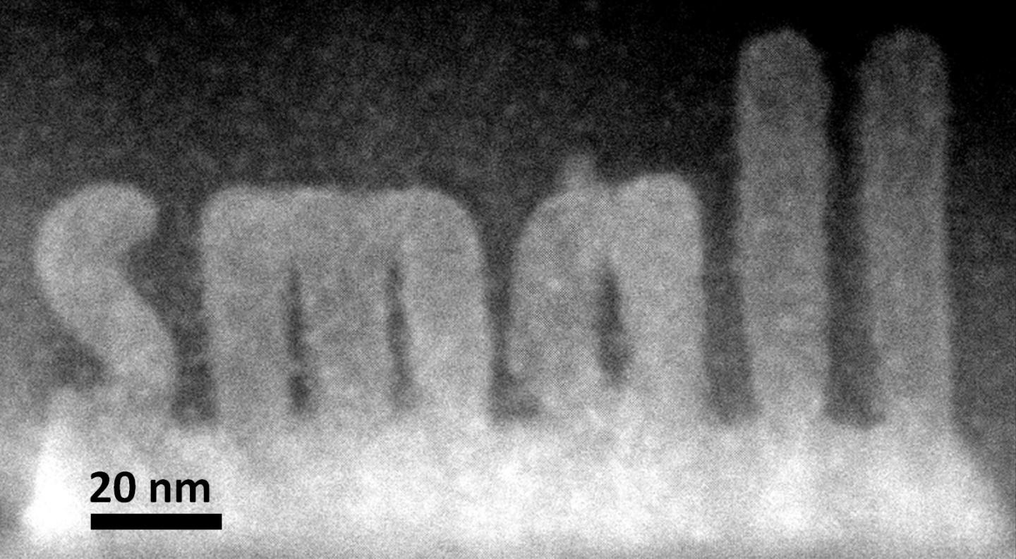
ORNL researchers used a new scanning transmission electron microscopy technique to sculpt 3-D nanoscale features in a complex oxide material. (credit: Department of Energy’s Oak Ridge National Laboratory)

Oak Ridge National Laboratory researchers have developed a way to build precision-sculpted 3-D strontium titanate nanostructures as small as one nanometer, using scanning transmission electron microscopes, which are normally used for imaging.

The technique could find uses in fabricating structures for functional nanoscale devices such as microchips. The structures grow epitaxially (in perfect crystalline alignment), which ensures that the same electrical and mechanical properties extend throughout the whole material, with more pronounced control over properties. The process can also be observed with atomic resolution.

The use of a scanning transmission electron microscope, which passes an electron beam through a bulk material, sets the approach apart from lithography techniques, which only pattern or manipulate a material’s surface. Combined with electron beam path control, the process could lead to large-scale implementation of bulk atomic-level fabrication as a new enabling tool of nanoscience and technology, providing a bottom-up, atomic-level complement to 3D printing, the researchers say.

“We’re using fine control of the beam to build something inside the solid itself,” said ORNL’s Stephen Jesse. “We’re making transformations that are buried deep within the structure. It would be like tunneling inside a mountain to build a house.”

The technique also offers a shortcut to researchers interested in studying how materials’ characteristics change with thickness. Instead of imaging multiple samples of varying widths, scientists could use the microscopy method to add layers to the sample and simultaneously observe what happens.

The study is published in the journal Small.


Abstract of Atomic-Level Sculpting of Crystalline Oxides: Toward Bulk Nanofabrication with Single Atomic Plane Precision

The atomic-level sculpting of 3D crystalline oxide nanostructures from metastable amorphous films in a scanning transmission electron microscope (STEM) is demonstrated. Strontium titanate nanostructures grow epitaxially from the crystalline substrate following the beam path. This method can be used for fabricating crystalline structures as small as 1–2 nm and the process can be observed in situ with atomic resolution. The fabrication of arbitrary shape structures via control of the position and scan speed of the electron beam is further demonstrated. Combined with broad availability of the atomic resolved electron microscopy platforms, these observations suggest the feasibility of large scale implementation of bulk atomic-level fabrication as a new enabling tool of nanoscience and technology, providing a bottom-up, atomic-level complement to 3D printing.

Disney Research-CMU design tool helps novices design 3-D-printable robotic creatures

Digital designs for robotic creatures are shown on the left and the physical prototypes produced via 3-D printing are on the right (credit: Disney Research, Carnegie Melon University)

Now you can design and build your own customized walking robot using a 3-D printer and off-the-shelf servo motors, with the help of a new DYI design tool developed by Disney Research and Carnegie Mellon University.

You can specify the shape, size, and number of legs for your robotic creature, using intuitive editing tools to interactively explore design alternatives. The system takes over much of the non-intuitive and tedious task of planning the motion of the robot, and ensures that your design is capable of moving the way you want and not fall down. Or you can alter your creature’s gait as desired.

Six robotic creatures designed with the Disney Research-CMU interactive design system: one biped, four quadrupeds and one five-legged robot (credit: Disney Research, Carnegie Melon University)

“Progress in rapid manufacturing technology is making it easier and easier to build customized robots, but designing a functioning robot remains a difficult challenge that requires an experienced engineer,” said Markus Gross, vice president of research for Disney Research. “Our new design system can bridge this gap and should be of great interest to technology enthusiasts and the maker community at large.”

The research team presented the system at SIGGRAPH Asia 2015, the ACM Conference on Computer Graphics and Interactive Techniques, in Kobe, Japan.

Design viewports

The design interface features two viewports: one that lets you edit the robot’s structure and motion and a second that displays how those changes would likely alter the robot’s behavior.

You can load an initial, skeletal description of the robot and the system then creates an initial geometry and places a motor at each joint position. You can then edit the robot’s structure, adding or removing motors, or adjust their position and orientation.

The researchers have developed an efficient optimization method that uses an approximate dynamics model to generate stable walking motions for robots with varying numbers of legs. In contrast to conventional methods that can require several minutes of computation time to generate motions, the process takes just a few seconds, enhancing the interactive nature of the design tool.

3-D printer-ready designs

Once the design process is complete, the system automatically generates 3-D geometry for all body parts, including connectors for the motors, which can then be sent to a 3-D printer for fabrication.

In a test of creating two four-legged robots, it took only minutes to design these creatures, but hours to assemble them and days to produce parts on 3-D printers,” said Bernhard Thomaszewski, a research scientist at Disney Research. “It is both expensive and time-consuming to build a prototype — which underscores the importance of a design system [that] produces a final design without the need for building multiple physical iterations.”

The research team also included roboticists at ETH Zurich. For more information, see Interactive Design of 3D-Printable Robotic Creatures (open access) and visit the project website.


Disney Research | Interactive Design of 3D Printable Robotic Creatures

Bitdrones: Interactive quadcopters allow for ‘programmable matter’ explorations

Could an interactive swarm of flying “3D pixels” (voxels) allow users to explore virtual 3D information by interacting with physical self-levitating building blocks? (credit: Roel Vertegaal)

We’ll find out Monday, Nov. 9, when Canadian Queen’s University’s Human Media Lab professor Roel Vertegaal and his students will unleash their “BitDrones” at the ACM Symposium on User Interface Software and Technology in Charlotte, North Carolina.

Programmable matter

Vertegaal believes his BitDrones invention is the first step towards creating interactive self-levitating programmable matter — materials capable of changing their 3D shape in a programmable fashion, using swarms of tiny quadcopters. Possible applications: real-reality 3D modeling, gaming, molecular modeling, medical imaging, robotics, and online information visualization.

“BitDrones brings flying programmable matter closer to reality,” says Vertegaal. “It is a first step towards allowing people to interact with virtual 3D objects as real physical objects.”

Vertegaal and his team at the Human Media Lab created three types of BitDrones, each representing self-levitating displays of distinct resolutions.

PixelDrones are equipped with one LED and a small dot matrix display. Users could physically explore a file folder by touching the folder’s associated PixelDrone, for example. When the folder opens, its contents are shown by other PixelDrones flying in a horizontal wheel below it. Files in this wheel are browsed by physically swiping drones to the left or right.

PixelDrone (credit: Roel Vertegaal)

ShapeDrones are augmented with a lightweight mesh and a 3D-printed geometric frame; they serve as building blocks for real-time, complex 3D models.

ShapeDrones (credit: Roel Vertegaal)

DisplayDrones are fitted with a curved flexible high-resolution touchscreen, a forward-facing video camera and Android smartphone board. Remote users could move around locally through a DisplayDrone with Skype for telepresence. A DisplayDrone can automatically track and replicate all of the remote user’s head movements, allowing a remote user to virtually inspect a location and making it easier for the local user to understand the remote user’s actions.

DisplayDrone (credit: Roel Vertegaal)

All three BitDrone types are equipped with reflective markers, allowing them to be individually tracked and positioned in real time via motion capture technology. The system also tracks the user’s hand motion and touch, allowing users to manipulate the voxels in space.

“We call this a ‘real reality’ interface rather than a virtual reality interface. This is what distinguishes it from technologies such as Microsoft HoloLens and the Oculus Rift: you can actually touch these pixels, and see them without a headset,” says Vertegaal.

The system currently only supports a dozen comparatively large 2.5 to 5 inch sized drones, but the team is working to scale up their system to support thousands of drones measuring under a half-inch in size, allowing users to render more seamless, high-resolution programmable matter.

Other forms of programmable matter

BitDrones are somewhat related to MIT Media Lab scientist Neil Gershenfeld’s “programmable pebbles” — reconfigurable robots that self-assemble into different configurations (see A reconfigurable miniature robot), MIT’s “swarmbots” — self-assembling swarming microbots that snap together into different shape (see MIT inventor unleashes hundreds of self-assembling cube swarmbots), J. Storrs Hall’s “utility fog” concept in which a swarm of nanobots, called “foglets,” can take the shape of virtually anything, and change shape on the fly (see Utility Fog: The Stuff that Dreams Are Made Of), and Autodesk Research’s Project Cyborg, a cloud-based meta-platform of design tools for programming matter across domains and scales.


Human Media Lab | BitDrones: Interactive Flying Microbots Show Future of Virtual Reality is Physical


Abstract of BitDrones: Towards Levitating Programmable Matter Using Interactive 3D Quadcopter Displays

In this paper, we present BitDrones, a platform for the construction of interactive 3D displays that utilize nano quadcopters as self-levitating tangible building blocks. Our prototype is a first step towards supporting interactive mid-air, tangible experiences with physical interaction techniques through multiple building blocks capable of physically representing interactive 3D data.

3D-printed microchannels deliver oxygen, nutrients from artery to tissue implant

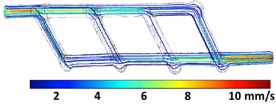
A miniature 3D-printed network of microchannels designed to link up an artery to a tissue implant to ensure blood flow of oxygen and nutrients. Inlet and outlet are ~1 millimeter in diameter; multiple smaller vessels are ~ 600 to 800 microns in diameter. Flow streamlines are color-coded corresponding to flow rate. Flow rate at the inlet is equal to 0.12 mL/min. (credit: Renganaden Sooppan et al./Tissue Engineering Part C: Methods)

Scientists have designed an innovative structure containing an intricate microchannel network of simulated blood vessels that solves one of the biggest challenges in regenerative medicine: How to deliver oxygen and nutrients to all cells in an artificial organ or tissue implant that takes days or weeks to grow in the lab prior to surgery.

The new study was performed by a research team led by Jordan Miller, assistant professor of bioengineering at Rice, and Pavan Atluri, assistant professor of surgery at Penn.

Stayin’ alive, stayin’ alive …

Miller explained that one of the hurdles of engineering large artificial tissues, such as livers or kidneys, is keeping the cells inside them alive. Tissue engineers have typically relied on the body’s own ability to grow blood vessels — for example, by implanting engineered tissue scaffolds inside the body and waiting for blood vessels from nearby tissues to spread via arbolization to the engineered constructs.

But that process can take weeks, and cells deep inside the constructs often starve or die from lack of oxygen before they’re reached by the slow-approaching blood vessels.

“What a surgeon needs in order to do transplant surgery isn’t just a mass of cells; the surgeon needs a vessel inlet and an outlet that can be directly connected to arteries and veins,” he said.

3D-printing pastry-inspired sugar glass to form an intricate microchannel capillary lattice

“We wondered if there were a way to implant a 3-D printed construct where we could connect host arteries directly to the construct and get perfusion [blood flow] immediately. In this study, we are taking the first step toward applying an analogy from transplant surgery to 3-D printed constructs we make in the lab.”

Miller turned to a method inspired by the intricate sugar glass cages crafted by pastry chefs to garnish desserts and that he had pioneered in 2012.

Description of sugar glass printing and initial flow testing. A: Extrusion print head in the process of printing a sugar glass lattice. B: Final sugar lattice prior to casting. The lattice contains a network of filaments supported by a surrounding well. Red line denotes the outer edge of the well that will be filled with PDMS silicone gel during casting. C: Schematic of printed sugar glass network. Drawing on the left denotes sugar filaments after printing, while the figure on the right shows trimmed filaments prior to casting. D: Final cast PDMS gel with microchannel network. (credit: Renganaden Sooppan et al./Tissue Engineering Part C: Methods)

Using an open-source 3-D printer to lay down individual filaments of sugar glass one layer at a time, the researchers printed a lattice of would-be blood vessels. Once the sugar hardened, they placed it in a mold and poured in silicone gel. After the gel cured, Miller’s team dissolved the sugar, leaving behind a network of small channels in the silicone.

“They don’t yet look like the blood vessels found in organs, but they have some of the key features relevant for a transplant surgeon,” Miller said. “We created a construct that has one inlet and one outlet, which are about 1 millimeter in diameter, and these main vessels branch into multiple smaller vessels, which are about 600 to 800 microns.”

Passing the surgeon-oriented test: normal blood flow

Collaborating surgeons at Penn in Atluri’s group then connected the inlet and outlet of the engineered gel to a major (femoral) artery in a small animal model. Using Doppler imaging technology, the team observed and measured blood flow through the construct and found that it withstood physiologic pressures and remained open and unobstructed for up to three hours.

They found that blood flowed normally through test constructs that were surgically connected to native blood vessels.

“This study provides a first step toward developing a transplant model for tissue engineering where the surgeon can directly connect arteries to an engineered tissue,” Miller said. “In the future, we aim to utilize a biodegradable material that also contains live cells next to these perfusable vessels for direct transplantation and monitoring long term.”
The report was published in an open-access paper in the journal Tissue Engineering Part C: Methods.

Abstract of Tissue Engineering Part C: Methods

The field of tissue engineering has advanced the development of increasingly biocompatible materials to mimic the extracellular matrix of vascularized tissue. However, a majority of studies instead rely on a multi-day inosculation between engineered vessels and host vasculature, rather than the direct connection of engineered microvascular networks with host vasculature. We have previously demonstrated that the rapid casting of 3D printed sacrificial carbohydrate glass is an expeditious and reliable method of creating scaffolds with 3D microvessel networks. Here, we describe a new surgical technique to directly connect host femoral arteries to patterned microvessel networks. Vessel networks were connected in vivo in a rat femoral artery graft model. We utilized laser Doppler imaging to monitor hind limb ischemia for several hours after implantation and thus measured the vascular patency of implants that were anastomosed to the femoral artery. This study may provide a method to overcome the challenge of rapid oxygen and nutrient delivery to engineered vascularized tissues implanted in vivo.
Minuscule, flexible compound lenses magnify large fields of view

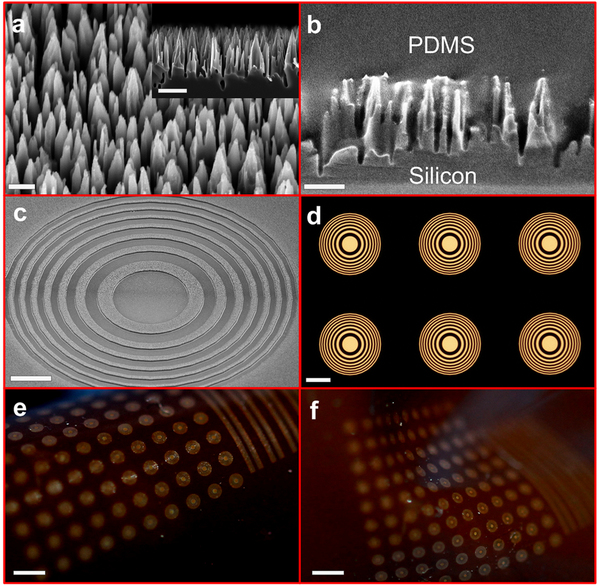
Tiny black silicon nanowire towers (a, b) make up dark regions of the flexible Fresnel zone lenses, minimizing unwanted reflections. Each individual lens resembles a bull’s-eye of alternating light and dark (c, d). Arrays of miniature lenses within a flexible polymer (e, f) can bend and stretch into different configurations. (credit: Hongrui Jiang)

Drawing inspiration from an insect’s multi-faceted eye, University of Wisconsin-Madison engineers have created miniature lenses with a vast range of vision. They’ve created the first flexible Fresnel zone plate microlenses with a wide field of view — a development that could allow everything from surgical scopes to security cameras and cell phones to capture a broader perspective at a fraction of the size required by conventional lenses.

Led by Hongrui Jiang, professor of electrical and computer engineering at UW-Madison, the researchers designed lenses no larger than the head of a pin and embedded them within flexible plastic. An array of the miniature lenses rolled into a cylinder can capture a panorama image covering a 170-degree field of view.

“We got the idea from compound eyes,” says Jiang, whose work was published in an open-access paper in the Oct. 30 issue of the journal Scientific Reports. “We know that multiple lenses on a domed structure give a large field of view.”

(a) Curved arrays of individual lenses (blue cylinder section) allow the tiny sensors to perceive a broader picture, bringing the Bucky mascot image into focus (c). The cylindrical arrangement shown in the schematic allowed researchers to resolve a 170-degree field of view. (credit: Hongrui Jiang)

The researchers can freely reconfigure the shape of the lens array, because rather than relying on conventional optics for focusing, they used Fresnel zone plates. Conventional lenses use refraction — the way light changes direction while passing through different substances (typically stiff, translucent ones, like glass) — to focus it on a single point. Instead, the Fresnel zone plates focus by diffraction — bending light as it passes the edge of a barrier.

Each of Jiang’s half-millimeter diameter lenses resembles a series of ripples on water emanating out from the splash of a stone. In bull’s-eye fashion, each concentric ring alternates between bright and dark. The distance between the rings determines the optical properties of the lens, and the researchers can tune those properties in a single lens by stretching and flexing it.

Previous attempts at creating Fresnel zone plate lenses have suffered from fuzzy vision. “The dark areas must be very dark,” explains Jiang, whose work is funded by the National Institutes of Health. “Essentially, it has to absorb the light completely. It’s hard to find a material that doesn’t reflect or transmit at all.”

Darker than dark

His team overcame this obstacle by using black silicon to trap light inside the dark regions of their Fresnel zone plate lenses. Black silicon consists of clusters of microscopic vertical pillars, or nanowires. Incoming light bouncing between individual silicon nanowires cannot escape the complex structure, making the material darker than dark.

Rather than laying down layers of black silicon on top of a clear backdrop, Jiang and his team took a bottom-up approach to generate their lenses. First they patterned aluminum rings on top of solid silicon wafers, and etched silicon nanowires in the areas between aluminum rings. Then they seeped a polymer between the silicon nanowire pillars. After the plastic support solidified, they etched away the silicon backing, leaving bull’s-eye patterned black silicon embedded in supple plastic.

This approach gave their lenses unprecedented crisp focusing capabilities, as well as the flexibility that enables them to capture a large field of view.

Jiang and his team are exploring ways to integrate the lenses into existing optical detectors and directly incorporate silicon electronic components into the lenses themselves.


Abstract of Micro-Fresnel-Zone-Plate Array on Flexible Substrate for Large Field-of-View and Focus Scanning

Field of view and accommodative focus are two fundamental attributes of many imaging systems, ranging from human eyes to microscopes. Here, we present arrays of Fresnel zone plates fabricated on a flexible substrate, which allows for the adjustment of both the field of view and optical focus. Such zone plates function as compact and lightweight microlenses and are fabricated using silicon nanowires. Inspired by compound eyes in nature, these microlenses are designed to point along various angles in order to capture images, offering an exceptionally wide field of view. Moreover, by flexing the substrate, the lens position can be adjusted, thus achieving axial focus scanning. An array of microlenses on a flexible substrate was incorporated into an optical system to demonstrate high resolution imaging of objects located at different axial and angular positions. These silicon based microlenses could be integrated with electronics and have a wide range of potential applications, from medical imaging to surveillance.

Graphene could take night-vision thermal imagers beyond ‘Predator’

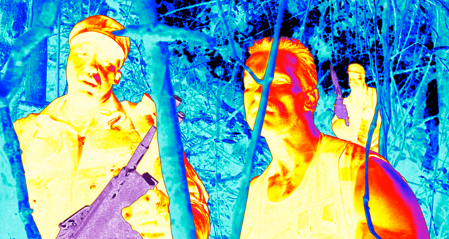
Alien’s view of soldiers in the movie Predator (credit: 20th Century Fox, altered by icyone)

In the 1987 movie “Predator,” an alien who sees in the far thermal infrared region of the spectrum hunts down Arnold Schwarzenegger and his team — introducing a generation of science-fiction fans to thermal imaging.

The ability of humans (or aliens) to see in the infrared allows military, police, firefighters, and others to do their jobs successfully at night and in smoky conditions. It also helps manufacturers and building inspectors identify overheating equipment or circuits. But currently, many of these systems require cryogenic cooling to filter out background radiation, or “noise,” to create a reliable image. That complicates the design and adds to the cost and the unit’s bulkiness and rigidity.

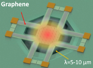
Schematic of graphene thermopile (credit: Allen L. Hsu et al./Nano Letters)

To find a more practical solution, researchers at MIT, Harvard, Army Research Laboratory, and University of California, Riverside, have developed an advanced device by integrating graphene with silicon microelectromechanical systems (MEMS) to make a flexible, transparent, and low-cost device for the mid-infrared range.

Testing showed it could be used to detect a person’s heat signature at room temperature (300 K or 27 degrees C/80 degrees F) without cryogenic cooling.

Future advances could make the device even more versatile. The researchers say that a thermal sensor could be based on a single layer of graphene, which would make it both transparent and flexible. Also, manufacturing could be simplified, which would bring costs down.

This work was reported in ACS journal Nano Letters. It has been supported in part by MIT/Army Institute for Soldier Nanotechnologies, Army Research Laboratories, Office of Naval Research GATE-MURI program, Solid State Solar Energy Conversion Center (S3TEC), MIT Center for Integrated Circuits and Systems, and Air Force Office of Scientific Research.

UPDATE Nov. 6, 2015: corrected wording to clarify that the device operates in the mid-infrared, not far-infrared range.


Abstract of Graphene-Based Thermopile for Thermal Imaging Applications

In this work, we leverage graphene’s unique tunable Seebeck coefficient for the demonstration of a graphene-based thermal imaging system. By integrating graphene based photothermo-electric detectors with micromachined silicon nitride membranes, we are able to achieve room temperature responsivities on the order of ∼7–9 V/W (at λ = 10.6 μm), with a time constant of ∼23 ms. The large responsivities, due to the combination of thermal isolation and broadband infrared absorption from the underlying SiN membrane, have enabled detection as well as stand-off imaging of an incoherent blackbody target (300–500 K). By comparing the fundamental achievable performance of these graphene-based thermopiles with standard thermocouple materials, we extrapolate that graphene’s high carrier mobility can enable improved performances with respect to two main figures of merit for infrared detectors: detectivity (>8 × 108 cm Hz1/2 W–1) and noise equivalent temperature difference (<100 mK). Furthermore, even average graphene carrier mobility (<1000 cm2 V–1 s–1) is still sufficient to detect the emitted thermal radiation from a human target.

3-D printed ‘building blocks’ of life

Images of printed embryonic stem cells, or embryoid bodies (credit: Liliang Ouyang et al./Biofabrication)

Chinese and U.S. scientists have developed a 3-D printing method capable of producing embryoid bodies — highly uniform “blocks” of embryonic stem cells. These cells, which are capable of generating all cell types in the body, could be used to build tissue structures and potentially even micro-organs.

The results were published Wednesday Nov. 4 in an open-access paper in the journal Biofabrication. “The embryoid body is uniform and homogenous, and serves as a much better starting point for further tissue growth,” explains Wei Sun, a lead author on the paper.

The researchers, based at Tsinghua University, Beijing, China, and Drexel University, Philadelphia, used extrusion-based 3-D printing to produce a grid-like 3-D structure to grow an embryoid body that demonstrated cell viability and rapid self-renewal for 7 days while maintaining high pluripotentcy.

“Two other common methods of printing these cells are two-dimensional (in a petri dish) or via the ‘suspension’ method [see 'Better bioprinting with stem cells'], where a ‘stalagmite’ of cells is built up by material being dropped via gravity,” said Sun. ”However, these don’t show the same cell uniformity and homogenous proliferation. I think that we’ve produced a 3-D microenvironment that is much more like that found in vivo for growing embryoid bodies, which explains the higher levels of cell proliferation.”

The researchers hope that this technique can be developed to produce embryoid bodies at high throughput, providing the basic building blocks for other researchers to perform experiments on tissue regeneration and/or for drug screening studies.

The researchers say the next step is to find out more about how to vary the size of the embryoid body by changing the printing and structural parameters, and how varying the embryoid body size leads to “manufacture” of different cell types.

“In the longer term, we’d like to produce controlled heterogeneous embryonic bodies,” said Sun. “This would promote different cell types developing next to each other, which would lead the way for growing micro-organs from scratch within the lab.”


Abstract of Three-dimensional bioprinting of embryonic stem cells directs highly uniform embryoid body formation

With the ability to manipulate cells temporarily and spatially into three-dimensional (3D) tissue-like construct, 3D bioprinting technology was used in many studies to facilitate the recreation of complex cell niche and/or to better understand the regulation of stem cell proliferation and differentiation by cellular microenvironment factors. Embryonic stem cells (ESCs) have the capacity to differentiate into any specialized cell type of the animal body, generally via the formation of embryoid body (EB), which mimics the early stages of embryogenesis. In this study, extrusion-based 3D bioprinting technology was utilized for biofabricating ESCs into 3D cell-laden construct. The influence of 3D printing parameters on ESC viability, proliferation, maintenance of pluripotency and the rule of EB formation was systematically studied in this work. Results demonstrated that ESCs were successfully printed with hydrogel into 3D macroporous construct. Upon process optimization, about 90% ESCs remained alive after the process of bioprinting and cell-laden construct formation. ESCs continued proliferating into spheroid EBs in the hydrogel construct, while retaining the protein expression and gene expression of pluripotent markers, like octamer binding transcription factor 4, stage specific embryonic antigen 1 and Nanog. In this novel technology, EBs were formed through cell proliferation instead of aggregation, and the quantity of EBs was tuned by the initial cell density in the 3D bioprinting process. This study introduces the 3D bioprinting of ESCs into a 3D cell-laden hydrogel construct for the first time and showed the production of uniform, pluripotent, high-throughput and size-controllable EBs, which indicated strong potential in ESC large scale expansion, stem cell regulation and fabrication of tissue-like structure and drug screening studies.