A battery alternative to costly, rare lithium

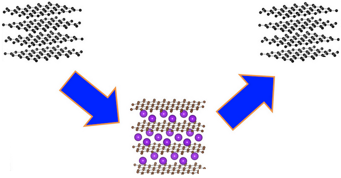
Potassium ions (purple) are compatible with graphite electrodes (black) and can function in a charge-discharge cycle, chemists have now shown (credit: Oregon State University)

Overturning nearly a century of a scientific dogma, Oregon State University chemists have now shown that  potassium could potentially replace rare, costly lithium in a new potassium-ion battery.

“For decades, people have assumed that potassium couldn’t work with graphite or other bulk carbon anodes in a battery,” said Xiulei (David) Ji, the lead author of the study and an assistant professor of chemistry in the College of Science at Oregon State University. “That assumption is incorrect,” he said. “It’s really shocking that no one ever reported on this issue for 83 years.”

The findings are important, the researchers say, because they open some new alternatives for batteries that can work with well-established, inexpensive graphite as the anode (the high-energy reservoir of electrons).

Lithium is quite rare, found in only 0.0017 percent, by weight, of the Earth’s crust. Because of that, it’s comparatively expensive, and also difficult to recycle.

Cost, availability problems with lithium

“The cost-related problems with lithium are sufficient that you won’t really gain much with economies of scale,” Ji said. “With most products, as you make more of them, the cost goes down. With lithium the reverse may be true in the near future. So we have to find alternatives.”

That alternative, he said, may be potassium, which is 880 times more abundant in the Earth’s crust than lithium. The new findings show that it can work effectively with graphite or soft carbon in the anode of an electrochemical battery.

“It’s safe to say that the energy density (amount of electrical power per unit volume) of a potassium-ion battery may never exceed that of lithium-ion batteries,” he said. But potassium-ion batteries may provide a “long cycling life, a high power density [ability to discharge quickly], a lot lower cost, and be ready to take the advantage of the existing manufacturing processes of carbon anode materials.”

Electrical energy storage in batteries is essential not only for consumer products such as cell phones and computers, but also in transportation, industry power backup, micro-grid storage, and for the wider use of renewable energy.

The Journal of the American Chemical Society published the findings from this discovery, which was supported by the U.S. Department of Energy. A patent is pending on the new technology.


Abstract of Carbon Electrodes for K-Ion Batteries

We for the first time report electrochemical potassium insertion in graphite in a nonaqueous electrolyte, which can exhibit a high reversible capacity of 273 mAh/g. Ex situ XRD studies confirm that KC36, KC24, and KC8 sequentially form upon potassiation, whereas depotassiation recovers graphite through phase transformations in an opposite sequence. Graphite shows moderate rate capability and relatively fast capacity fading. To improve the performance of carbon K-ion anodes, we synthesized a nongraphitic soft carbon that exhibits cyclability and rate capability much superior to that of graphite. This work may open up a new paradigm toward rechargeable K-ion batteries.

A realistic bio-inspired robotic finger

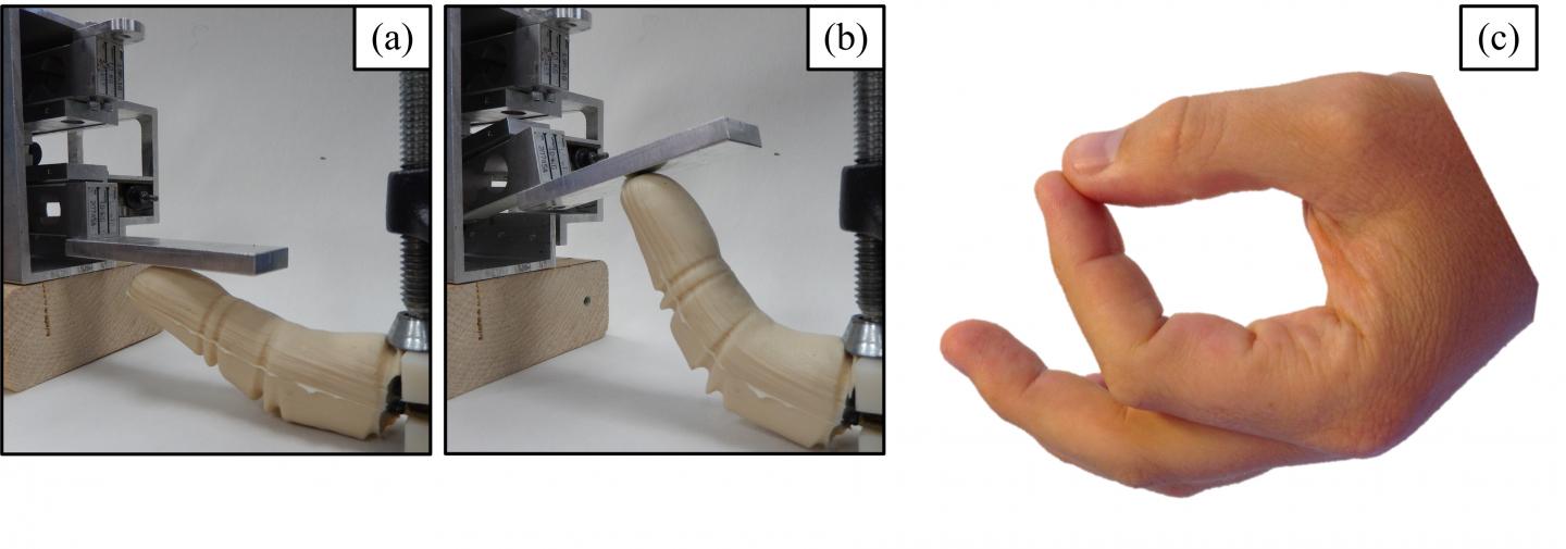
Heating and cooling a 3D-printed shape memory alloy to operate a robotic finger (credit: Florida Atlantic University/Bioinspiration & Biomimetics)

A realistic 3D-printed robotic finger using a shape memory alloy (SMA) and a unique thermal training technique has been developed by Florida Atlantic University assistant professor Erik Engeberg, Ph.D.

“We have been able to thermomechanically train our robotic finger to mimic the motions of a human finger, like flexion and extension,” said Engeberg. “Because of its light weight, dexterity and strength, our robotic design offers tremendous advantages over traditional mechanisms, and could ultimately be adapted for use as a prosthetic device, such as on a prosthetic hand.”

Most robotic parts used today are rigid, have a limited range of motion and don’t look lifelike.

In the study, described in an open-access article in the journal Bioinspiration & Biomimetics, Engeberg and his team used a resistive heating process called “Joule” heating that involves the passage of electric currents through a conductor that releases heat.

How to create a robotic finger

  • The researchers first downloaded a 3-D computer-aided design (CAD) model of a human finger from the Autodesk 123D website (under creative commons license).
  • With a 3-D printer, they created the inner and outer molds that housed a flexor and extensor actuator and a position sensor. The extensor actuator takes a straight shape when it’s heated and the flexor actuator takes a curved shape when heated.
  • They used SMA plates and a multi-stage casting process to assemble the finger.
  • Electric currents flow through each SMA actuator from an electric power source at the base of the finger as a heating and cooling process to operate the robotic finger.

Results from the study showed a rapid flexing and extending motion of the finger and ability to recover its trained shape accurately and completely, confirming the biomechanical basis of its trained shape.

Initial use in underwater robotics

“Because SMAs require a heating process and cooling process, there are challenges with this technology, such as the lengthy amount of time it takes for them to cool and return to their natural shape, even with forced air convection,” said Engeberg. So they used the technology for underwater robotics, which would provide a rapid-cooling environment.

Engeberg used thermal insulators at the fingertip, which were kept open to facilitate water flow inside the finger. As the finger flexed and extended, water flowed through the inner cavity within each insulator to cool the actuators.

“Because our robotic finger consistently recovered its thermomechanically trained shape better than other similar technologies, our underwater experiments clearly demonstrated that the water cooling component greatly increased the operational speed of the finger,” said Engeberg.

Undersea applications using Engeberg’s new technology could help to address some of the difficulties and challenges humans encounter while working in ocean depths.


FAU – BioRobotics Lab | Bottle Pick and Drop Demo UR10 and Shadow Hand


FAU – BioRobotics Lab | Simultaneous Grasp Synergies Controlled by EMG


FAU – BioRobotics Lab | Shadow Hand and UR10 – Grab Bottle, Pour Liquid


Abstract of Anthropomorphic finger antagonistically actuated by SMA plates

Most robotic applications that contain shape memory alloy (SMA) actuators use the SMA in a linear or spring shape. In contrast, a novel robotic finger was designed in this paper using SMA plates that were thermomechanically trained to take the shape of a flexed human finger when Joule heated. This flexor actuator was placed in parallel with an extensor actuator that was designed to straighten when Joule heated. Thus, alternately heating and cooling the flexor and extensor actuators caused the finger to flex and extend. Three different NiTi based SMA plates were evaluated for their ability to apply forces to a rigid and compliant object. The best of these three SMAs was able to apply a maximum fingertip force of 9.01N on average. A 3D CAD model of a human finger was used to create a solid model for the mold of the finger covering skin. Using a 3D printer, inner and outer molds were fabricated to house the actuators and a position sensor, which were assembled using a multi-stage casting process. Next, a nonlinear antagonistic controller was developed using an outer position control loop with two inner MOSFET current control loops. Sine and square wave tracking experiments demonstrated minimal errors within the operational bounds of the finger. The ability of the finger to recover from unexpected disturbances was also shown along with the frequency response up to 7 rad s−1. The closed loop bandwidth of the system was 6.4 rad s−1 when operated intermittently and 1.8 rad s−1 when operated continuously.

Smaller silver nanoparticles more likely to be absorbed by aquatic life, UCLA study finds

Researchers studied zebrafish because they have some genetic similarities to humans and their embryos and larvae are transparent, which makes them easier to observe (credit: Tunde Akinloye/CNSI)

A study led by UCLA scientists has found that smaller silver nanoparticles entered fish’s bodies more deeply and persisted longer than larger silver nanoparticles or fluid silver nitrate.

More than 2,000 consumer products today contain nanoparticles — particles so small that they are measured in billionths of a meter. Manufacturers use nanoparticles to help sunscreen work better against the sun’s rays and to make athletic apparel better at wicking moisture away from the body, among many other purposes.

Of those products, 462 contain nanoparticles made from silver, which are used for their ability to kill bacteria. But that benefit might be coming at a cost to the environment. In many cases, simply using the products as-intended causes silver nanoparticles to wind up in rivers and other bodies of water, where they can be ingested by fish and interact with other marine life.

The new study by the University of California Center for Environmental Implications of Nanotechnology, published online in the journal ACS Nano, was intend to begin addressing the question: to what extent do organisms retain those particles and what effects might they have?

Absorption of silver nanoparticles by fish

According to Andre Nel, director of UCLA’s Center for Environmental Implications of Nanotechnology (CEIN) and associate director of the California NanoSystems Institute at UCLA, it is not yet known whether silver nanoparticles are harmful, but the research team wanted to first identify whether they were even being absorbed by fish.

Deposits of 20-nanometer silver nanoparticles in zebrafish gill filaments (outlined in red) (credit: Olivia J. Osborne et al./ACS Nano)

In the study, researchers placed zebrafish in water that contained fluid silver nitrate and two sizes of silver nanoparticles — some measuring 20 nanometers in diameter and others 110 nanometers. The researchers found that the two sizes of particles affected the fish very differently.

The researchers used zebrafish in the study because they have some genetic similarities to humans, and their embryos and larvae are transparent (which makes them easier to observe). In addition, they tend to absorb chemicals and other substances from water.

The team focused its research on the fish’s gills and intestines because they are the organs most susceptible to silver exposure.

The gills showed a significantly higher silver content for the 20-nanometer than the 110-nanometer particles, while the values were more similar in the intestines; both sizes of the silver particles were retained in the intestines even after the fish spent seven days in clean water.

The experiment was one of the most comprehensive in vivo studies to date on silver nanoparticles, as well as the first to compare silver nanoparticle toxicity by extent of organ penetration and duration with different-sized particles, and the first to demonstrate a mechanism for the differences.

Osborne said the results seem to indicate that smaller particles penetrated deeper into the fishes’ organs and stayed there longer because they dissolve faster than the larger particles and are more readily absorbed by the fish.

Nel said the team’s next step is to determine whether silver particles are potentially harmful. “Our research will continue in earnest to determine what the long-term effects of this exposure can be,” he said.

The research was supported by the National Science Foundation and the Environmental Protection Agency.


Abstract of Organ-Specific and Size-Dependent Ag Nanoparticle Toxicity in Gills and Intestines of Adult Zebrafish

We studied adult zebrafish to determine whether the size of 20 and 110 nm citrate-coated silver nanoparticles (AgC NPs) differentially impact the gills and intestines, known target organs for Ag toxicity in fish. Following exposure for 4 h, 4 days, or 4 days plus a 7 day depuration period, we obtained different toxicokinetic profiles for different particle sizes, as determined by Ag content of the tissues. Ionic AgNO3 served as a positive control. The gills showed a significantly higher Ag content for the 20 nm particles at 4 h and 4 days than the 110 nm particles, while the values were more similar in the intestines. Both particle types were retained in the intestines even after depuration. These toxicokinetics were accompanied by striking size-dependent differences in the ultrastructural features and histopathology in the target organs in response to the particulates. Ag staining of the gills and intestines confirmed prominent Ag deposition in the basolateral membranes for the 20 nm but not for the 110 nm particles. Furthermore, it was possible to link the site of tissue deposition to disruption of the Na+/K+ ion channel, which is also localized to the basolateral membrane. This was confirmed by a reduction in ATPase activity and immunohistochemical detection of the α subunit of this channel in both target organs, with the 20 nm particles causing significantly higher inhibition and disruption than the larger size particles or AgNO3. These results demonstrate the importance of particle size in determining the hazardous impact of AgNPs in the gills and intestines of adult zebrafish.

Vertical ‘light antennas’ grown from organic semiconductor crystals

In full bloom: A scanning electron microscopy image of a vertical tetraanaline semiconductor crystal (credit: Jessica Wang)

Materials scientists from the California NanoSystems Institute at UCLA have discovered a way to make organic (carbon-based) semiconductors more powerful and efficient by creating “light antennas.” The thin, pole-like devices could absorb light from all directions, an improvement over today’s wide, flat panels that can only absorb light from one surface.

The breakthrough was in creating an improved structure for one type of organic semiconductor: a building block of a conductive polymer called tetraaniline (TANI). The scientists showed for the first time that tetraaniline crystals could be grown vertically.

The study, led by Richard Kaner, distinguished professor of chemistry and biochemistry and materials science and engineering, was recently published online by the journal ACS Nano.

Growing vertical organic semiconductors

Scanning electron microscope image showing TANI crystals oriented vertically based on graphene (credit: Yue Wang et al./ACS Nano)

The UCLA team grew the tetraaniline crystals vertically from a substrate made of graphene, so the crystals stood up like spikes instead of lying flat as they do when produced using current techniques. Scientists had previously grown crystals vertically in inorganic semiconducting materials, including silicon, but doing it in organic materials has been more difficult.

Tetraaniline is a desirable material for semiconductors because of its particular electrical and chemical properties, which are determined by the orientation of very small crystals it contains. Devices such as solar cells, photosensors, and supercapacitors would work better if the crystals grew vertically because vertical crystals can be packed more densely in the semiconductor, making it more powerful and more efficient at controlling electrical current.

Kaner and his colleagues also developed a one-step method for growing highly ordered, vertically aligned crystals for a variety of organic semiconductors using the same graphene substrate. “This technique enables us to pattern crystals wherever we want,” he said. “You could make electronic devices from these semiconductor crystals and grow them precisely in intricate patterns required for the device you want, such as thin-film transistors or light-emitting diodes.”

The research was supported by the Boeing Company, the National Science Foundation, the U.S. Department of Energy, and the Defense Threat Reduction Agency.


Abstract of Graphene-Assisted Solution Growth of Vertically Oriented Organic Semiconducting Single Crystals

Vertically oriented structures of single crystalline conductors and semiconductors are of great technological importance due to their directional charge carrier transport, high device density, and interesting optical properties. However, creating such architectures for organic electronic materials remains challenging. Here, we report a facile, controllable route for producing oriented vertical arrays of single crystalline conjugated molecules using graphene as the guiding substrate. The arrays exhibit uniform morphological and crystallographic orientations. Using an oligoaniline as an example, we demonstrate this method to be highly versatile in controlling the nucleation densities, crystal sizes, and orientations. Charge carriers are shown to travel most efficiently along the vertical interfacial stacking direction with a conductivity of 12.3 S/cm in individual crystals, the highest reported to date for an aniline oligomer. These crystal arrays can be readily patterned and their current harnessed collectively over large areas, illustrating the promise for both micro- and macroscopic device applications.

Method to replace silicon with carbon nanotubes developed by IBM Research

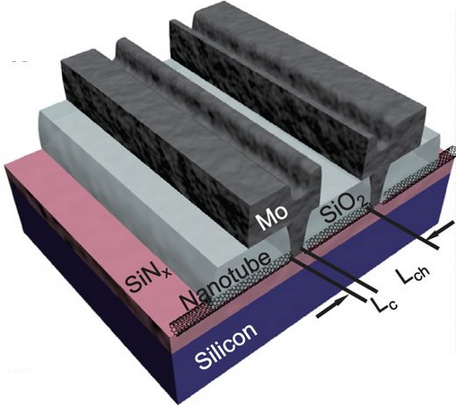
Schematic of a set of molybdenum (M0) end-contacted nanotube transistors (credit: Qing Cao et al./Science)

IBM Research has announced a “major engineering breakthrough” that could lead to carbon nanotubes replacing silicon transistors in future computing technologies.

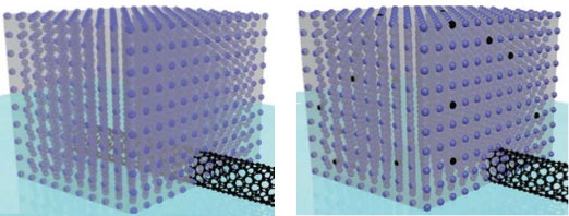
As transistors shrink in size, electrical resistance increases within the contacts, which impedes performance. So IBM researchers invented a metallurgical process similar to microscopic welding that chemically binds the contact’s metal (molybdenum) atoms to the carbon atoms at the ends of nanotubes.

The new method promises to shrink transistor contacts without reducing performance of carbon-nanotube devices, opening a pathway to dramatically faster, smaller, and more powerful computer chips beyond the capabilities of traditional silicon semiconductors.

“This is the kind of breakthrough that we’re committed to making at IBM Research via our $3 billion investment over 5 years in research and development programs aimed a pushing the limits of chip technology,” said Dario Gil, VP, Science & Technology, IBM Research. “Our aim is to help IBM produce high-performance systems capable of handling the extreme demands of new data analytics and cognitive computing applications.”

The development was reported today in the October 2 issue of the journal Science.

Overcoming contact resistance

Schematic of carbon nanotube transistor contacts. Left: High-resistance side-bonded contact, where the single-wall nanotube (SWNT) (black tube) is partially covered by the metal molybdenum (Mo) (purple dots). Right: low-resistance end-bonded contact, where the SWNT is attached to the molybdenum electrode through carbide bonds, while the carbon atoms (black dots) from the originally covered portion of the SWNT uniformly diffuse out into the Mo electrode (credit: Qing Cao et al./Science)

The new “end-bonded contact scheme” allows carbon-nanotube contacts to be shrunken down to below 10 nanometers without deteriorating performance. IBM says the scheme could overcome contact resistance challenges all the way to the 1.8 nanometer node and replace silicon with carbon nanotubes.

Silicon transistors have been made smaller year after year, but they are approaching a point of physical limitation. With Moore’s Law running out of steam, shrinking the size of the transistor — including the channels and contacts — without compromising performance has been a challenge for researchers for decades.

Single wall carbon nanotube (credit: IBM)

IBM has previously shown that carbon nanotube transistors can operate as excellent switches at channel dimensions of less than ten nanometers, which is less than half the size of today’s leading silicon technology. Electrons in carbon transistors can move more easily than in silicon-based devices and use less power.

Carbon nanotubes are also flexible and transparent, making them useful for flexible and stretchable electronics or sensors embedded in wearables.

IBM acknowledges that several major manufacturing challenges still stand in the way of commercial devices based on nanotube transistors.

Earlier this summer, IBM unveiled the first 7 nanometer node silicon test chip, pushing the limits of silicon technologies.


First optical ‘rectenna’ converts light to DC current

This schematic shows the components of the optical rectenna developed at the Georgia Institute of Technology (credit: Thomas Bougher, Georgia Tech)

Using nanometer-scale components, Georgia Institute of Technology researchers have demonstrated the first optical rectenna, a device that combines the functions of an antenna and a rectifier diode to convert light directly into DC current.

Based on multiwall carbon nanotubes and tiny rectifiers fabricated onto them, the optical rectennas could provide a new technology for energy harvesters, including photodetectors that would operate without the need for cooling, convert waste heat to electricity,  and ultimately, efficiently capture solar energy.

In the new devices, the carbon nanotubes act as antennas to capture light from the Sun or other sources. As the waves of light hit the nanotube antennas, they create an oscillating charge that moves through rectifier devices attached to them. The rectifiers switch on and off at record high petahertz speeds, creating a small direct current.

The efficiency of the devices demonstrated so far remains below one percent, but the researchers hope to boost that output by using billions of rectennas in an array, which could produce significant current. They believe a rectenna with commercial potential may be available within a year.

“We could ultimately make solar cells that are twice as efficient at a cost that is ten times lower, and that is to me an opportunity to change the world in a very big way” said Baratunde Cola, an associate professor in the George W. Woodruff School of Mechanical Engineering at Georgia Tech. “As a robust, high-temperature detector, these rectennas could be a completely disruptive technology if we can get to one percent efficiency. If we can get to higher efficiencies, we could apply it to energy conversion technologies and solar energy capture.”

A carbon nanotube optical rectenna converts green laser light to electricity in the laboratory of Baratunde Cola at the Georgia Institute of Technology (credit: Rob Felt, Georgia Tech)

“A rectenna is basically an antenna coupled to a diode, but when you move into the optical spectrum, that usually means a nanoscale antenna coupled to a metal-insulator-metal diode,” Cola explained. “The closer you can get the antenna to the diode, the more efficient it is. So the ideal structure uses the antenna as one of the metals in the diode – which is the structure we made.”

The rectennas fabricated by Cola’s group are grown on rigid substrates, but the goal is to grow them on a foil or other material that would produce flexible solar cells or photodetectors.

Cola sees the rectennas built so far as simple proof of principle. “We think we can reduce the resistance by several orders of magnitude just by improving the fabrication of our device structures,” he said. “Based on what others have done and what the theory is showing us, I believe that these devices could get to greater than 40 percent efficiency.”

The research, supported by the Defense Advanced Research Projects Agency (DARPA), the Space and Naval Warfare (SPAWAR) Systems Center and the Army Research Office (ARO), is reported September 28 in the journal Nature Nanotechnology.

* Developed in the 1960s and 1970s, rectennas have operated at wavelengths as short as ten micrometers, but for more than 40 years researchers have been attempting to make devices at optical wavelengths. There were many challenges: making the antennas small enough to couple optical wavelengths, and fabricating a matching rectifier diode small enough and able to operate fast enough to capture the electromagnetic wave oscillations. But the potential of high efficiency and low cost kept scientists working on the technology.

Fabricating the rectennas begins with growing forests of vertically-aligned carbon nanotubes on a conductive substrate. Using atomic layer chemical vapor deposition, the nanotubes are coated with an aluminum oxide material to insulate them. Finally, physical vapor deposition is used to deposit optically-transparent thin layers of calcium then aluminum metals atop the nanotube forest. The difference of work functions between the nanotubes and the calcium provides a potential of about two electron volts, enough to drive electrons out of the carbon nanotube antennas when they are excited by light.

In operation, oscillating waves of light pass through the transparent calcium-aluminum electrode and interact with the nanotubes. The metal-insulator-metal junctions at the nanotube tips serve as rectifiers switching on and off at femtosecond intervals, allowing electrons generated by the antenna to flow one way into the top electrode. Ultra-low capacitance, on the order of a few attofarads, enables the 10-nanometer diameter diode to operate at these exceptional frequencies.


Georgia Tech | Using nanometer-scale components, researchers have demonstrated the first optical rectenna, a device that combines the functions of an antenna and a rectifier diode to convert light directly into DC current.


Abstract of A carbon nanotube optical rectenna

An optical rectenna—a device that directly converts free-propagating electromagnetic waves at optical frequencies to direct current—was first proposed over 40 years ago, yet this concept has not been demonstrated experimentally due to fabrication challenges at the nanoscale. Realizing an optical rectenna requires that an antenna be coupled to a diode that operates on the order of 1 pHz (switching speed on the order of 1 fs). Diodes operating at these frequencies are feasible if their capacitance is on the order of a few attofarads, but they remain extremely difficult to fabricate and to reliably couple to a nanoscale antenna. Here we demonstrate an optical rectenna by engineering metal–insulator–metal tunnel diodes, with a junction capacitance of ∼2 aF, at the tip of vertically aligned multiwalled carbon nanotubes (∼10 nm in diameter), which act as the antenna. Upon irradiation with visible and infrared light, we measure a d.c. open-circuit voltage and a short-circuit current that appear to be due to a rectification process (we account for a very small but quantifiable contribution from thermal effects). In contrast to recent reports of photodetection based on hot electron decay in a plasmonic nanoscale antenna, a coherent optical antenna field appears to be rectified directly in our devices, consistent with rectenna theory. Finally, power rectification is observed under simulated solar illumination, and there is no detectable change in diode performance after numerous current–voltage scans between 5 and 77 °C, indicating a potential for robust operation.
How to make 3-D objects totally disappear

This image shows a 3-D illustration of a metasurface skin cloak made from an ultrathin layer of nanoantennas (gold blocks) covering an arbitrarily shaped object. When activated, light reflects off the cloak (red arrows) as if it were reflecting off a flat mirror. (credit: Image courtesy of Xiang Zhang group, Berkeley Lab/UC Berkeley)

An ultra-thin invisibility “skin” cloak that can conform to the shape of an object and conceal it from detection with visible light has been developed by scientists at Lawrence Berkeley National Laboratory (Berkeley Lab) and the University of California (UC) Berkeley.

Working with blocks of gold nanoantennas, the Berkeley researchers created a “skin cloak” just 80 nanometers in thickness that was wrapped around a three-dimensional object about the size of a few biological cells and shaped with multiple bumps and dents. The surface of the skin cloak was meta-engineered to reflect light waves, making the object invisible to optical detection when the cloak is activated.

“This is the first time a 3D object of arbitrary shape has been cloaked from visible light,” said Xiang Zhang, director of Berkeley Lab’s Materials Sciences Division. “Our ultra-thin cloak now looks like a coat. It is easy to design and implement, and is potentially scalable for hiding macroscopic objects.”

Zhang, who holds the Ernest S. Kuh Endowed Chair at UC Berkeley and is a member of the Kavli Energy NanoSciences Institute at Berkeley (Kavli ENSI), is the corresponding author of a paper describing this research in the journal Science.

Click to see an animation of an invisibility cloak that makes a 3-D object disappear (credit: Zhang group)

It is the scattering of light from its interaction with matter that enables us to detect and observe objects. The rules that govern these interactions in natural materials can be circumvented in metamaterials, whose optical properties arise from their physical structure rather than their chemical composition.

For the past ten years, Zhang and his research group have been pushing the boundaries of how light interacts with metamaterials, managing to curve the path of light or bend it backwards, phenomena not seen in natural materials, and to render objects optically undetectable. In the past, their metamaterial-based optical carpet cloaks were bulky and hard to scale up, and entailed a phase difference between the cloaked region and the surrounding background that made the cloak itself detectable, though what it concealed was not.

Now you see it, now you don’t

In the new study, the researchers used red light to illuminate an arbitrarily shaped 3-D sample object about 1,300 square micrometers in area and wrapped in the gold nanoantenna skin cloak. The light reflected off the surface of the skin cloak was identical to light reflected off a flat mirror, making the object underneath it invisible even by phase-sensitive detection. The cloak can be turned “on” or “off” simply by switching the polarization of the nanoantennas.

“A phase shift provided by each individual nanoantenna fully restores both the wavefront and the phase of the scattered light so that the object remains perfectly hidden,” says co-lead author Zi Jing Wong, also a member of Zhang’s research group.

According the researchers. the ability to manipulate the interactions between light and metamaterials offers future prospects for technologies such as high-resolution optical microscopes and superfast optical computers, and for hiding the detailed layout of microelectronic components or for security encryption purposes.

At the macroscale, among other applications, invisibility cloaks could prove useful for 3D displays, they add.


Abstract of An ultrathin invisibility skin cloak for visible light

Metamaterial-based optical cloaks have thus far used volumetric distribution of the material properties to gradually bend light and thereby obscure the cloaked region. Hence, they are bulky and hard to scale up and, more critically, typical carpet cloaks introduce unnecessary phase shifts in the reflected light, making the cloaks detectable. Here, we demonstrate experimentally an ultrathin invisibility skin cloak wrapped over an object. This skin cloak conceals a three-dimensional arbitrarily shaped object by complete restoration of the phase of the reflected light at 730-nanometer wavelength. The skin cloak comprises a metasurface with distributed phase shifts rerouting light and rendering the object invisible. In contrast to bulky cloaks with volumetric index variation, our device is only 80 nanometer (about one-ninth of the wavelength) thick and potentially scalable for hiding macroscopic objects.

These self-propelled microscopic carbon-capturing motors may reduce carbon-dioxide levels in oceans

Nanoengineers have invented tiny tube-shaped micromotors that zoom around in water and efficiently remove carbon dioxide. The surfaces of the micromotors are functionalized with the enzyme carbonic anhydrase, which enables the motors to help rapidly convert carbon dioxide to calcium carbonate. (credit: Laboratory for Nanobioelectronics, UC San Diego Jacobs School of Engineering)

Nanoengineers at the University of California, San Diego have designed enzyme-functionalized micromotors the size of red blood cells that rapidly zoom around in water, remove carbon dioxide, and convert it into a usable solid form.

The proof-of-concept study represents a promising route to mitigate the buildup of carbon dioxide, a major greenhouse gas in the environment, said the researchers.

The team, led by distinguished nanoengineering professor and chair Joseph Wang, published the work this month in the journal Angewandte Chemie.

In their experiments, the nanoengineers demonstrated that the micromotors rapidly decarbonated water solutions that were saturated with carbon dioxide. Within five minutes, the micromotors removed 90 percent of the carbon dioxide from a solution of deionized water.

The micromotors were just as effective in a sea-water solution and removed 88 percent of the carbon dioxide in the same time frame.

“In the future, we could potentially use these micromotors as part of a water treatment system, like a water decarbonation plant,” said Kevin Kaufmann, an undergraduate researcher in Wang’s lab and a co-author of the study.

The micromotors are essentially six-micrometer-long tubes that help rapidly convert carbon dioxide into calcium carbonate, a solid mineral found in eggshells, the shells of various marine organisms, calcium supplements and cement. The micromotors have an outer polymer surface that holds the enzyme carbonic anhydrase, which speeds up the reaction between carbon dioxide and water to form bicarbonate. Calcium chloride, which is added to the water solutions, helps convert bicarbonate to calcium carbonate.

The fast, continuous motion of the micromotors in solution makes the micromotors extremely efficient at removing carbon dioxide from water, according to the researchers. The team explained that the micromotors’ autonomous movement induces efficient solution mixing, leading to faster carbon dioxide conversion.

Self-propulsion from oxygen gas bubbles

To fuel the micromotors in water, researchers added hydrogen peroxide, which reacts with the inner platinum surface of the micromotors to generate a stream of oxygen gas bubbles that propel the micromotors around. When released in water solutions containing as little as two to four percent hydrogen peroxide, the micromotors reached speeds of more than 100 micrometers per second.

Vdeo frames showing the movement of a micromotor in sea water (credit: Laboratory for Nanobioelectronics, UC San Diego Jacobs School of Engineering)

However, the use of hydrogen peroxide as the micromotor fuel is a drawback because it is an extra additive and requires the use of expensive platinum materials to build the micromotors. As a next step, researchers are planning to make carbon-capturing micromotors that can be propelled by water.

“If the micromotors can use the environment as fuel, they will be more scalable, environmentally friendly and less expensive,” said Kaufmann.


Abstract of Micromotor-Based Biomimetic Carbon Dioxide Sequestration: Towards Mobile Microscrubbers

We describe a mobile CO2 scrubbing platform that offers a greatly accelerated biomimetic sequestration based on a self-propelled carbonic anhydrase (CA) functionalized micromotor. The CO2 hydration capability of CA is coupled with the rapid movement of catalytic micromotors, and along with the corresponding fluid dynamics, results in a highly efficient mobile CO2 scrubbing microsystem. The continuous movement of CA and enhanced mass transport of the CO2 substrate lead to significant improvements in the sequestration efficiency and speed over stationary immobilized or free CA platforms. This system is a promising approach to rapid and enhanced CO2 sequestration platforms for addressing growing concerns over the buildup of greenhouse gas.

DNA-based nanodevices for molecular medicine: an overview

Virus-protein-coated DNA origami nanostructures. With the help of protein encapsulation, DNA origamis can be transported into human cells much more efficiently. (credit: Veikko Linko and Mauri Kostiainen)

KurzweilAI has covered a wide variety of research projects that explore how DNA molecules can be assembled into complex nanostructures for molecular-scale diagnostics, smart drug-delivery, and other uses. For example, tailored DNA structures could find targeted cancer cells and release their molecular payload (drugs or antibodies) selectively.

An article written by researchers from Aalto University just published in Trends in Biotechnology journal, comparing biological DNA-nanomachine developments and their uses, should help put this varied research in perspective.

The authors explain that “the field of structural DNA nanotechnology started around 30 years ago when Ned Seeman performed pioneering research with DNA junctions and lattice. … The key player in the fast development of DNA nanotechnology was the invention of DNA origami in 2006. The DNA origami method is based on folding a long
single-stranded ‘DNA scaffold strand’ into a customized shape with a set of short synthetic strands that act as ‘staples’ to bind the overall structure together.”

“This method is the starting point for practically all other straightforward design approaches available today,” says Veikko Linko, an Academy of Finland postdoctoral researcher from Biohybrid Materials Group and first author.

The accurate shape of a DNA origami nanostructure can be used to create entirely metallic nanoparticles on silicon substrates. (credit: Veikko Linko, Boxuan Shen and Mauri Kostiainen with permission from Royal Society of Chemistry)

Versatile DNA nanostructures

The most important feature of a DNA-based nanostructure is its modularity, the authors note. DNA structures can be fabricated with nanometer-precision, and other molecules such as RNA, proteins, peptides and drugs can be anchored to them with the same resolution.

Such a high precision can be exploited in creating nanosized optical devices as well as molecular platforms and bar codes for various imaging techniques and analytics.

The author further point out that for molecular medicine, DNA-based devices could be used for detecting single molecules and modulating cell signaling. In the near future, highly sophisticated DNA robots could even be used in creating artificial immune systems, they note.

In addition, a system based on tailored DNA devices could help to avoid unnecessary drug treatments, since programmed DNA-nanorobots could detect various agents from the blood stream, and immediately start the battle against disease.


Abstract of DNA Nanostructures as Smart Drug-Delivery Vehicles and Molecular Devices

DNA molecules can be assembled into custom predesigned shapes via hybridization of sequence-complementary domains. The folded structures have high spatial addressability and a tremendous potential to serve as platforms and active components in a plethora of bionanotechnological applications. DNA is a truly programmable material, and its nanoscale engineering thus opens up numerous attractive possibilities to develop novel methods for therapeutics. The tailored molecular devices could be used in targeting cells and triggering the cellular actions in the biological environment. In this review we focus on the DNA-based assemblies – primarily DNA origami nanostructures – that could perform complex tasks in cells and serve as smart drug-delivery vehicles in, for example, cancer therapy, prodrug medication, and enzyme replacement therapy.

Pushing the resolution and exposure-time limits of lensless imaging

With “coherent diffraction imaging,” extreme ultraviolet light scatters off a sample and produces a diffraction pattern, which a computer then analyzes to reconstruct an image of the target material (credit: Dr. Michael Zürch, Friedrich Schiller University Jena, Germany)

Physicists at Friedrich Schiller University in Germany are pushing the boundaries of nanoscale imaging by shooting ultra-high-resolution, real-time images in extreme ultraviolet light — without lenses. The new method could be used to study everything from semiconductor chips to cancer cells, the scientists say.

They are improving a lensless imaging technique called “coherent diffraction imaging,” which has been around since the 1980s. To take a picture with this method, scientists fire an extreme ultraviolet laser or X-ray at a target. The light scatters off, and some of those photons interfere with one another and find their way onto a detector, creating a diffraction pattern.

Diffraction pattern of red laser beam (credit: Wisky/Wikipedia)

By analyzing that pattern, a computer then reconstructs the path those photons must have taken, which generates an image of the target material.

But the quality of the images depends on the radiation source. Traditionally, researchers have used big, powerful X-ray beams like the one at the SLAC National Accelerator Laboratory, which can pump out lots of photons.

To make the process more accessible, researchers have developed smaller machines using coherent laser-like beams, which are cheaper but produce lower-quality images and require short focal lengths (similar to placing a specimen close to a microscope to boost the magnification) and long exposure times.

As in conventional photography, that rules out large, real-time images.

Now, Michael Zürch and his research team have built an ultrafast laser that fires extreme UV photons 100 times faster than previous table-top machines and is able to snap an image at a resolution of 26 nanometers (the size of a blackline walnut virus) — almost the theoretical diffraction limit for the 33-nanometers UV light used. They were also able to get real-time images at a rate of one per second at the reduced resolution of 80 nanometers.

The prospect of high-resolution, real-time imaging using a relatively low-cost, small setup could lead to all kinds of applications, Zürch said. Engineers could use this to hunt for tiny defects in semiconductor chips. Biologists could zoom in on the organelles that make up a cell. Eventually, he said, the researchers might be able to reach shorter exposure times and higher resolution levels.

The team will present their work at Frontiers in Optics, the Optical Society’s annual meeting and conference in San Jose, California on October 22, 2015.