’4-D’ printing technology allows self-folding of complex ‘transformer’ objects, using smart shape-memory materials

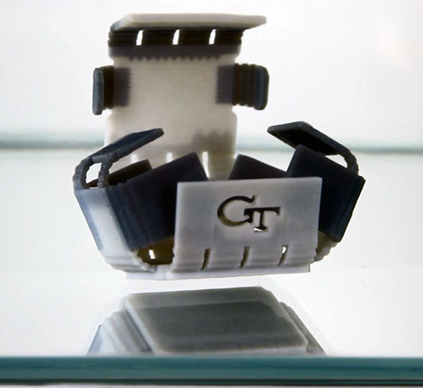
This image shows the self-folding process of smart shape-memory materials with slightly different responses to heat. Using materials that fold at slightly different rates ensures that the components do not interfere with one another during the process. (credit: Qi Laboratory)

Using components made from smart shape-memory materials (which can return to their original shape) with slightly different responses to heat, researchers have demonstrated a “four-dimensional” printing technology that allows for creating complex, self-folding structures.

The technology, developed by researchers at the Georgia Institute of Technology and the Singapore University of Technology and Design (SUTD), could be used to create 3-D structures that sequentially fold themselves from components that had been flat or rolled into a tube for shipment. To achieve that, the components could be designed to respond to stimuli such as temperature, moisture or light in a way that is precisely timed to create space structures, deployable medical devices, robots, toys, and a range of other structures.

Shape memory polymers

The researchers used smart shape memory polymers (SMPs) with the ability to remember one shape and change to another programmed shape when uniform heat is applied. Creating objects that change shape in a controlled sequence over time is enabled by printing multiple materials with different dynamic mechanical properties in prescribed patterns throughout the 3-D object.

When these components are then heated, each SMP responds at a different rate to change its shape, depending on its own internal clock. By carefully timing these changes, 3-D objects can be programmed to self-assemble in desired ways.

The research creates self-folding structures from 3-D printed patterns containing varying amounts of different smart shape-memory polymers. The patterning, done with a 3-D printer, allows the resulting flat components to have varying temporal response to the same stimuli.*

The team demonstrated the approach with a series of examples, including a mechanism that can be switched from a flat strip into a locked configuration as one end and controllably bends and threads itself through a keyhole. They also demonstrated a flat sheet that can fold itself into a 3-D box with interlocking flaps. These examples all require precise control of the folding sequence of different parts of the structure to avoid collisions of the components during folding.**

Using a 3-D printer, researchers produce smart shape-memory materials with slightly different responses to heat. Heat from water in a tank activates the materials and begins the self-folding process. (Credit: Qi Laboratory, Georgia Tech)

“We have exploited the ability to 3-D print smart polymers and integrate as many as ten different materials precisely into a 3-D structure,” said Martin L. Dunn, a professor at Singapore University of Technology and Design who is also the director of the SUTD Digital Manufacturing and Design Centre. “We are now extending this concept of digital SMPs to enable printing of SMPs with dynamic mechanical properties that vary continuously in 3-D space.”

Morphing aircraft

The research team envisions a broad range of applications for their technology. For example, an unmanned air vehicle might change shape from one designed for a cruise mission to one designed for a dive. Also possible would be 3-D components designed to fold flat or be rolled up into tubes so they could be easily transported, and then later deformed into their intended 3D configuration for use.

The research was reported September 8 in an open-access paper in the journal Scientific Reports. The work is funded by the U.S. Air Force Office of Scientific Research, the U.S. National Science Foundation, and the Singapore National Research Foundation.

* “Previous efforts to create sequential shape changing components involved placing multiple heaters at specific regions in a component and then controlling the on-and-off time of individual heaters,” explained Jerry Qi, a professor in the George W. Woodruff School of Mechanical Engineering at Georgia Tech. “This earlier approach essentially requires controlling the heat applied throughout the component in both space and time and is complicated. We turned this approach around and used a spatially uniform temperature which is easier to apply and then exploited the ability of different materials to internally control their rate of shape change through their molecular design.”

** The team used companion finite element simulations to predict the responses of the 3-D printed components, which were made from varying ratios of two different commercially available shape-memory polymers. A simplified reduced-order model was also developed to rapidly and accurately describe the physics of the self-folding process. “An important aspect of self-folding is the management of self-collisions, where different portions of the folding structure contact and then block further folding,” the researchers said in their paper. “A metric is developed to predict collisions and is used together with the reduced-order model to design self-folding structures that lock themselves into stable desired configurations.”


Abstract of Sequential Self-Folding Structures by 3D Printed Digital Shape Memory Polymers

Folding is ubiquitous in nature with examples ranging from the formation of cellular components to winged insects. It finds technological applications including packaging of solar cells and space structures, deployable biomedical devices, and self-assembling robots and airbags. Here we demonstrate sequential self-folding structures realized by thermal activation of spatially-variable patterns that are 3D printed with digital shape memory polymers, which are digital materials with different shape memory behaviors. The time-dependent behavior of each polymer allows the temporal sequencing of activation when the structure is subjected to a uniform temperature. This is demonstrated via a series of 3D printed structures that respond rapidly to a thermal stimulus, and self-fold to specified shapes in controlled shape changing sequences. Measurements of the spatial and temporal nature of self-folding structures are in good agreement with the companion finite element simulations. A simplified reduced-order model is also developed to rapidly and accurately describe the self-folding physics. An important aspect of self-folding is the management of self-collisions, where different portions of the folding structure contact and then block further folding. A metric is developed to predict collisions and is used together with the reduced-order model to design self-folding structures that lock themselves into stable desired configurations.

3-D printing lightweight, flexible multiple materials in real time, including electronic circuits

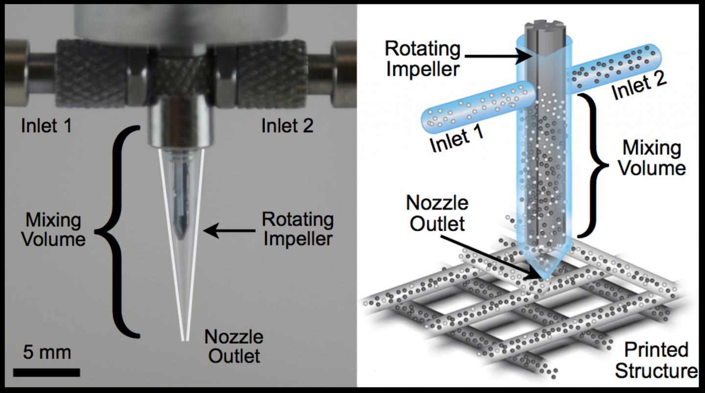
Multiple-materials printer. Each fluid enters the mixing chamber through a separate inlet and is mixed in a narrow gap by an impeller rotating at a constant rate. Optical image (left) and schematic illustration (right) of impeller-based mixing nozzle. (credit: Thomas Ober, Harvard SEAS/Wyss Institute)

Harvard researchers have designed new printheads for 3-D printers that can simultaneously handle multiple materials with different properties, allowing for 3-D printing wearable devices, flexible electronics, and soft robots.

To print a flexible device, including the electronics, a 3-D printer must be able to seamlessly transition from a flexible material that moves with the wearer’s joints for wearable applications, to a rigid material that accommodates the electronic components. It would also need to be able to embed electrical circuitry using multiple inks of varying conductivity and resistivity, and precisely switching between them while changing composition and geometry.  And do it all in real time.

How this will change 3-D printing

The researchers say they have designed a new multimaterial printhead that do all of the above. It can handle a wide range of complex fluids by using a rotating impeller inside a microscale nozzle, seamlessly printing combinations of materials and processes that were not formerly possible:

  • Mixed conductive and resistive inks to embed electrical circuitry inside 3D printed objects.
  • Multiple inks within a single nozzle, eliminating the structural defects that often occur during the start-and-stop process of switching materials.
  • Silicone elastomers, with gradient architectures composed of soft and rigid regions.
  • Reactive materials, such as two-part epoxies, which typically harden quickly when the two parts are combined (think: Krazy glue).

The research was led by Jennifer A. Lewis, the Hansjörg Wyss Professor of Biologically Inspired Engineering at the Harvard John A. Paulson School of Engineering and Applied Sciences (SEAS) and a Core Faculty Member at the Wyss Institute for Biologically Inspired Engineering at Harvard. The work was published in an open-access paper in Proceedings of the National Academy of Sciences (PNAS). It was supported by the Department of Energy Energy Frontier Research Center on Light-Material Interactions in Energy Conversion, the Intelligence Community Postdoctoral Fellowship program, and the Society in Science Branco-Weiss Foundation.

“The recent work by the Lewis Group is a significant advancement to the field of additive manufacturing,” said Christopher Spadaccini, Director of the Center for Engineered Materials, Manufacturing and Optimization at Lawrence Livermore National Lab. “By allowing for the mixing of two highly viscous materials on the fly, the promise of mixed material systems with disparate mechanical and functional properties becomes much more realistic.  Before, this was really only a concept.  This work will be foundational for applications which [require] integrated electrical and structural materials.”


Abstract of Active mixing of complex fluids at the microscale

Mixing of complex fluids at low Reynolds number is fundamental for a broad range of applications, including materials assembly, microfluidics, and biomedical devices. Of these materials, yield stress fluids (and gels) pose the most significant challenges, especially when they must be mixed in low volumes over short timescales. New scaling relationships between mixer dimensions and operating conditions are derived and experimentally verified to create a framework for designing active microfluidic mixers that can efficiently homogenize a wide range of complex fluids. Active mixing printheads are then designed and implemented for multimaterial 3D printing of viscoelastic inks with programmable control of local composition.

3D-printed silicone guide with chemical cues helps regenerate complex nerves after injury

3-D scans of a nerve from different angles are used to create a custom regeneration guide for complex nerves (credit: University of Minnesota)

A national team of researchers used a combination of 3-D imaging and 3-D printing techniques to create a custom silicone guide implanted with biochemical cues to help nerve regeneration after an injury.

Nerve regeneration is a complex process, which is why regrowth of nerves after injury or disease is very rare and often permanent, according to the Mayo Clinic.

As a test, the researchers used a 3-D scanner to reverse-engineer the structure of a rat’s sciatic nerve. They then used a specialized, custom-built 3-D printer to print a regeneration guide containing 3D-printed chemical cues to promote both motor and sensory nerve regeneration within the same structure. The guide was then implanted into the rat by surgically grafting it to the cut ends of the nerve. Within about 10 to 12 weeks, the rat’s ability to walk again was improved.

A 3D-printed complex nerve-regeneration pathway implanted in a rat helped to improve walking in 10 to 12 weeks after implantation (credit: University of Minnesota)

“Someday we hope that we could have a 3D scanner and printer right at the hospital to create custom nerve guides right on site to restore nerve function,” said University of Minnesota mechanical engineering professor Michael McAlpine, the study’s lead researcher.

Conventional nerve guidance channels are typically fabricated around cylindrical substrates, so the resulting guidance devices are limited to linear structures. This is is the first time a study has shown the creation of a custom guide for regrowth of a complex nerve like the Y-shaped sciatic nerve, which has both sensory and motor branches.

“The exciting next step would be to implant these guides in humans rather than rats,” McAlpine said. For cases where a patient’s nerve is unavailable for scanning, McAlpine said there could someday be a “library” of scanned nerves from other people or cadavers that hospitals could use to create closely matched 3D-printed guides for patients.

The study by researchers from the University of Minnesota, Virginia Tech, University of Maryland, Princeton University, and Johns Hopkins University was published Thursday (Sept. 17) in the journal Advanced Functional Materials.


UMN College of Science and Engineering | 3D printing of a nerve regeneration guide [no audio]


Abstract of 3D Printed Anatomical Nerve Regeneration Pathways

A 3D printing methodology for the design, optimization, and fabrication of a custom nerve repair technology for the regeneration of complex peripheral nerve injuries containing bifurcating sensory and motor nerve pathways is introduced. The custom scaffolds are deterministically fabricated via a microextrusion printing principle using 3D models, which are reverse engineered from patient anatomies by 3D scanning. The bifurcating pathways are augmented with 3D printed biomimetic physical cues (microgrooves) and path-specific biochemical cues (spatially controlled multicomponent gradients). In vitro studies reveal that 3D printed physical and biochemical cues provide axonal guidance and chemotractant/chemokinetic functionality. In vivo studies examining the regeneration of bifurcated injuries across a 10 mm complex nerve gap in rats showed that the 3D printed scaffolds achieved successful regeneration of complex nerve injuries, resulting in enhanced functional return of the regenerated nerve. This approach suggests the potential of 3D printing toward advancing tissue regeneration in terms of: (1) the customization of scaffold geometries to match inherent tissue anatomies; (2) the integration of biomanufacturing approaches with computational modeling for design, analysis, and optimization; and (3) the enhancement of device properties with spatially controlled physical and biochemical functionalities, all enabled by the same 3D printing process.

Ultrafast ‘electron camera’ visualizes atomic ripples in 2-D material

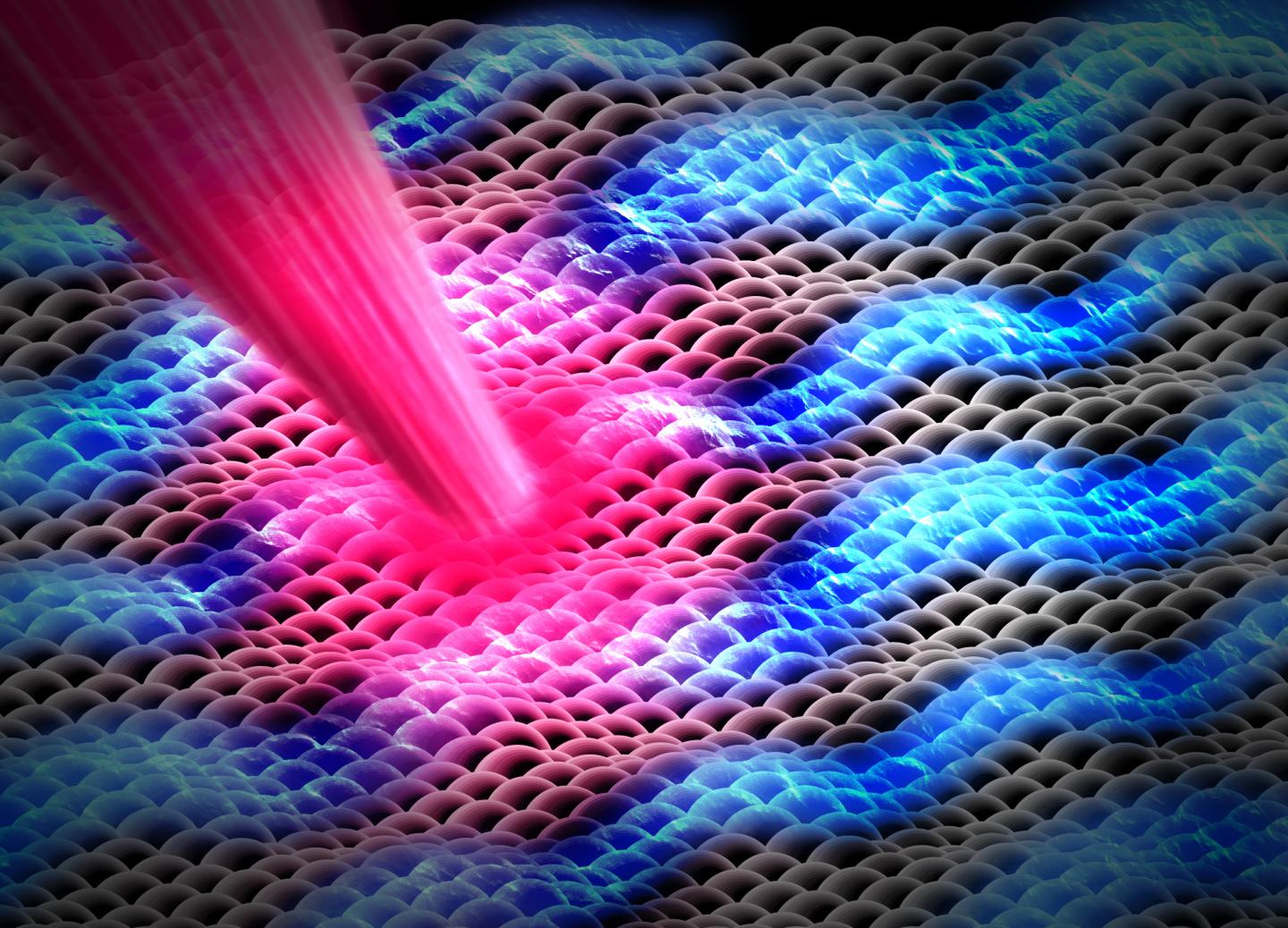
Researchers have used SLAC’s “electron cameras” to take snapshots of a three-atom-thick layer of a promising material called molybdenum disulfide as it wrinkles in response to a laser pulse. Understanding these dynamic ripples could provide crucial clues for the development of next-generation solar cells, electronics, and catalysts. (credit: SLAC National Accelerator Laboratory)

A new “electron camera” can capture images of individual moving atoms as they form wrinkles on a three-atom-thick material and in trillionths of a second — one of the world’s fastest. It has been developed by scientists from the Department of Energy’s SLAC National Accelerator Laboratory and Stanford University.

This unprecedented level of detail could guide researchers in developing more efficient solar cells, fast and flexible nanoelectronics, and high-performance chemical catalysts.

The breakthrough, published Aug. 31 in Nano Letters, was made possible by SLAC’s instrument for ultrafast electron diffraction (UED), which uses energetic electrons to take snapshots of atoms and molecules.

SLAC National Accelerator Laboratory | This animation explains how researchers use high-energy electrons at SLAC to study faster-than-ever motions of atoms and molecules relevant to important materials properties and chemical processes.

Extraordinary 2-D materials

Monolayers, or 2-D materials, contain just a single layer of molecules. In this form, they can take on new and exciting properties, such as superior mechanical strength and an extraordinary ability to conduct electricity and heat. But how do these monolayers acquire their unique characteristics? Until now, researchers only had a limited view of the underlying mechanisms.

A representative electron diffraction pattern from monolayer Molybdenum disulfide (MoS2) taken with the new SLAC electron camera, showing the crystalline nature of the sample (credit: (credit: SLAC National Accelerator Laboratory)

“The functionality of 2-D materials critically depends on how their atoms move,” said SLAC and Stanford researcher Aaron Lindenberg, who led the research team.

“However, no one has ever been able to study these motions on the atomic level and in real time before. Our results are an important step toward engineering next-generation devices from single-layer materials.”

The research team looked at molybdenum disulfide, or MoS2, which is widely used as a lubricant but takes on a number of interesting behaviors when in single-layer form.

For example, the monolayer form is normally an insulator, but when stretched, it can become electrically conductive. This switching behavior could be used to function like transistors in thin, flexible electronics and to encode information in data-storage devices.

Thin films of MoS2 are also under study as possible catalysts that facilitate chemical reactions. In addition, they capture light very efficiently and could be used in future solar cells.

Because of this strong interaction with light, researchers also think they may be able to manipulate the material’s properties with light pulses.

“To engineer future devices, control them with light, and create new properties through systematic modifications, we first need to understand the structural transformations of monolayers on the atomic level,” said Stanford researcher Ehren Mannebach, the study’s lead author.

Electron camera reveals ultrafast motions

Previous analyses showed that single layers of molybdenum disulfide have a wrinkled surface. However, these studies only provided a static picture. The new study reveals for the first time how surface ripples form and evolve in response to laser light.

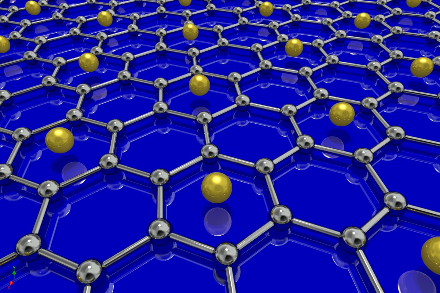
Visualization of laser-induced motions of atoms (black and yellow spheres) in a molybdenum disulfide monolayer: The laser pulse creates wrinkles with large amplitudes — more than 15 percent of the layer’s thickness — that develop in a trillionth of a second. (credit: K.-A. Duerloo/Stanford)

Researchers at SLAC placed their monolayer samples, which were prepared by Linyou Cao’s group at North Carolina State University, into a beam of very energetic electrons. The electrons, which come bundled in ultrashort pulses, scatter off the sample’s atoms and produce a signal on a detector that scientists use to determine where atoms are located in the monolayer. This technique is called ultrafast electron diffraction.

The team then used ultrashort laser pulses to excite motions in the material, which cause the scattering pattern to change over time.

To study ultrafast atomic motions in a single layer of molybdenum disulfide, researchers followed a pump-probe approach: They excited motions with a laser pulse (pump pulse, red) and probed the laser-induced structural changes with a subsequent electron pulse (probe pulse, blue). The electrons of the probe pulse scatter off the monolayer’s atoms (blue and yellow spheres) and form a scattering pattern on the detector — a signal the team used to determine the monolayer structure. By recording patterns at different time delays between the pump and probe pulses, the scientists were able to determine how the atomic structure of the molybdenum disulfide film changed over time. (credit: SLAC National Accelerator Laboratory)

“Combined with theoretical calculations, these data show how the light pulses generate wrinkles that have large amplitudes — more than 15 percent of the layer’s thickness — and develop extremely quickly, in about a trillionth of a second. This is the first time someone has visualized these ultrafast atomic motions,” Lindenberg said.

Once scientists better understand monolayers of different materials, they could begin putting them together and engineer mixed materials with completely new optical, mechanical, electronic and chemical properties.

The research was supported by DOE’s Office of Science, the SLAC UED/UEM program development fund, the German National Academy of Sciences, and the U.S. National Science Foundation.


Abstract of Dynamic Structural Response and Deformations of Monolayer MoS2 Visualized by Femtosecond Electron Diffraction

Two-dimensional materials are subject to intrinsic and dynamic rippling that modulates their optoelectronic and electromechanical properties. Here, we directly visualize the dynamics of these processes within monolayer transition metal dichalcogenide MoS2 using femtosecond electron scattering techniques as a real-time probe with atomic-scale resolution. We show that optical excitation induces large-amplitude in-plane displacements and ultrafast wrinkling of the monolayer on nanometer length-scales, developing on picosecond time-scales. These deformations are associated with several percent peak strains that are fully reversible over tens of millions of cycles. Direct measurements of electron–phonon coupling times and the subsequent interfacial thermal heat flow between the monolayer and substrate are also obtained. These measurements, coupled with first-principles modeling, provide a new understanding of the dynamic structural processes that underlie the functionality of two-dimensional materials and open up new opportunities for ultrafast strain engineering using all-optical methods.

Japanese paper art inspires new 3-D fabrication method that goes beyond 3-D printing limitations

A new assembly method based on an ancient Japanese paper art quickly transforms 2-D structures into complex 3-D shapes. The results, reported by a Northwestern University and University of Illinois research team, could be useful in tissue engineering and microelectromechanical systems. (credit: University of Illinois)

A research team has created complex 3-D micro- and nanostructures out of silicon and other materials used in advanced technologies by employing a new assembly method that uses a Japanese Kirigami paper-cutting method.

The method builds on the team’s “pop-up” fabrication technique — going from a 2-D material to 3-D in an instant, like a pop-up children’s book — reported in January this year on KurzweilAI and in the journal Science. Those earlier ribbon-like structures yielded open networks, with limited ability to achieve closed-form shapes or to support more complex spatially extended devices.

In their new work, the research team at Northwestern University, University of Illinois and Tsinghua University solved this problem by borrowing ideas from Kirigami, the ancient Japanese technique for forming paper structures by folding and cutting. The Kirigami study was published last week (Sept. 8) in the Proceedings of the National Academy of Sciences (PNAS).

Two-dimensional precursors, finite-element analysis predictions, and scanning electron microscope images for five 3-D membrane–ribbon hybrid mesostructures (credit: Yihui Zhang et al./PNAS)

Starting with 2-D structures formed using state-of-the-art methods in semiconductor manufacturing and carefully placed “Kirigami cuts,” the researchers created more than 50 different mostly closed 3-D structures that, in theory, could contain cells or support advanced electronic or optoelectronic devices. The structures also suggest use in tissue engineering and industrial applications, such as biomedical devices, energy storage and microelectromechanical systems.

Creating 3-D pop-ups by cutting at strain points

“The key concept in Kirigami is a cut,” said Yonggang Huang, the Walter P. Murphy Professor of Civil and Environmental Engineering and Mechanical Engineering at Northwestern’s McCormick School of Engineering. “Cuts usually lead to failure, but here we have the opposite: cuts allow us to produce complex 3-D shapes we wouldn’t have otherwise,” he said. “This unique 3-D fabrication technique now can be used by others for their own creations and applications.”

Huang and his team worked with the research group of John A. Rogers, the Swanlund Chair and professor of materials science and engineering at the University of Illinois. Rogers and Huang are co-corresponding authors of the study.

The research team made 3-D structures from materials including silicon, polymers, metals and dielectrics. Some structures combined a number of materials, such as gold and a semiconductor, including patterns that provide useful optical responses.

The Kirigami technique is suitable for mass production, and the breadth of materials that can be manipulated illustrates its usefulness over 3-D printing, which is generally only applied with polymers, the researchers suggest. The Kirigami method also is fast, while 3-D printing is slow.

The researchers started with a flat material adhered at certain places to a stretched substrate. They strategically made “cuts” in the material so that when the stretch is released and the surface “pops up” into three-dimensions, all the physical strain from the new 3-D shape is released through the cuts, keeping the structure from breaking. The cuts are made in just those places where strain normally would be concentrated.

Computer simulations

The “cuts” are not made physically in the material, Huang explained. Instead, methods based on manufacturing approaches for computer chips allow these features to be defined in the material with extremely high engineering control. The researchers successfully predicted by computer simulation the 2-D shape and cuts needed to produce the actual 3-D structure. The ability to make predictions eliminates the time and expense of trial-and-error experiments.

The sizes of the 3-D structures range from 100 nanometers square to 3 centimeters square while the cuts themselves are typically between 1 micron and 10 microns wide for silicon 3-D structures — small enough to interface directly with cells or intracellular structures or to manipulate components in microelectronics.

The researchers also can reversibly tune the optical properties of their structures by mechanical stretching, after they are formed. They demonstrated a simple optical shutter based on arrays of rotating microplates, operating much like shutters on a window.


Abstract of A mechanically driven form of Kirigami as a route to 3D mesostructures in micro/nanomembranes

Assembly of 3D micro/nanostructures in advanced functional materials has important implications across broad areas of technology. Existing approaches are compatible, however, only with narrow classes of materials and/or 3D geometries. This paper introduces ideas for a form of Kirigami that allows precise, mechanically driven assembly of 3D mesostructures of diverse materials from 2D micro/nanomembranes with strategically designed geometries and patterns of cuts. Theoretical and experimental studies demonstrate applicability of the methods across length scales from macro to nano, in materials ranging from monocrystalline silicon to plastic, with levels of topographical complexity that significantly exceed those that can be achieved using other approaches. A broad set of examples includes 3D silicon mesostructures and hybrid nanomembrane–nanoribbon systems, including heterogeneous combinations with polymers and metals, with critical dimensions that range from 100 nm to 30 mm. A 3D mechanically tunable optical transmission window provides an application example of this Kirigami process, enabled by theoretically guided design.

Cancer patient receives 3D-printed ribs in world-first surgery

(Credit: Anatomics)

A Spanish cancer patient has received a 3D-printed titanium sternum and rib cage.

Suffering from a chest wall sarcoma (a type of cancerous tumor that grows, in this instance, around the rib cage), the 54 year old man needed his sternum and a portion of his rib cage replaced. This part of the chest is notoriously tricky to recreate with prosthetics, due to the complex geometry and design required for each patient.

Thoracic surgeons typically use flat and plate implants for the chest. However, these can come loose over time and increase the risk of complications. The patient’s surgical team at the Salamanca University Hospital thought a fully customized 3D-printed implant could replicate the intricate structures of the sternum and ribs, providing a safer option for the patient.

So they turned to Melbourne-based medical device company Anatomics, which designed and manufactured the implant using the Melbourne CSIRO 3D printing facility.

Using high resolution CT (computed tomography) data, the Anatomics team was able to create a 3-D reconstruction of the chest wall and tumor, allowing the surgeons to plan and accurately define resection margins. Twelve days after the surgery, the patient was discharged and has recovered well.


CSIRO | Cancer patient receives 3D printed ribs in world first surgery

How curly nanowires can absorb more light to power nanoscale electronic circuits

This illustration shows a prototype  device comprising bare nanospring photodetectors placed on a glass substrate, with metal contacts to collect charges (credit: Tural Khudiyev and Mehmet Bayindir/Applied Optics)

Researchers from Bilkent University, Ankara, Turkey, have shown that twisting straight nanowires into springs can increase the amount of light the wires absorb by up to 23 percent. Absorbing more light is important because one application of nanowires is turning light into electricity, for example, to power tiny sensors instead of requiring batteries.

If nanowires are made from a semiconductor like silicon, light striking the wire will dislodge electrons from the crystal lattice, leaving positively charged “holes” behind. Both the electrons and the holes move through the material to generate electricity. The more light the wire absorbs; the more electricity it generates. (A device that converts light into electricity can function as either a solar cell or a photosensor.)

In 2007, U.S. researchers introduced a single nanowire photosensor that produced enough electricity from sunlight (up to 200 picowatts) to power nanoscale electronic circuits. More recently, a European researcher team built a nanowire solar cell with almost 14 percent efficiency from the compounds of indium and phosphorus. This efficiency is not enough to beat the best crystalline silicon solar cells on the market, but because nanowires can cover more area with less material, the nanowire solar cells could ultimately be cheaper.

“There is huge potential in the area of nanoscale photosensors,” said Mehmet Bayindir, Director, National Nanotechnology Research Center, Bilkent University. “More efficient outputs might induce the emergence of a new generation of photosensor technology and eventual commercialization of these products.”

Mie resonances increase current flow

Bayindir and his colleague Tural Khudiyev, now a postdoctoral associate at The Massachusetts Institute of Technology, have found that adjusting the geometry of the typical nanowire may be one way to realize the desired efficiency enhancement.

Nanowires are usually long, thin and straight. Their tiny dimensions mean they interact with light differently than ordinary materials. Certain wavelengths of light will match up in just the right way with the dimensions of the nanowire, causing the light to “resonate” or bounce around inside the wire.

These “Mie resonances” are especially advantageous at the nanoscale, Khudiyev said. The resonances are named after the early-20th-century German physicist Gustav Mie, who developed equations to describe why tiny metal particles make stained glass windows glow so brightly.

Mie resonances will occur with straight nanowires, but by twisting the nanowire into a helical shape, the researchers found they could take double advantage of the phenomena. “When the nanospring period matches the Mie resonance points, a ‘double resonance’ condition occurs, which boosts light harvesting efficiency,” Khudiyev said.

Additionally, twisting the wire upwards shortened its length, reducing the required area by up to 50 percent.

Nanoscale sensors

The enhanced light harvesting efficiency of nanosprings opens new opportunities to build nanoscale devices that power themselves, such as sensors to detect environmental toxins or to monitor the structural integrity of a bridge.

“Our nanospring shape induces more power output both in the broad spectrum range and at some desired single point (which can be engineered easily), and these make powering of more advanced nanosystems possible with a single nanospring-based photovoltaics system,” Khudiyev said.

“Experimental observation of a nanospring-based photosensor design and its integration into a large-scale fiber embedded system would be interesting as the next steps,” Bayindir said.

The group has already developed an easy way to produce nanosprings by first making long nanowire arrays, then heating them to a temperature at which the arrays can be twisted into the nanospring shape. The technique can be varied to control the diameter of the spring and the tightness of the curl.

The results of this research are published in the journal Applied Optics, from The Optical Society (OSA).


Abstract of Nanosprings harvest light more efficiently

Nanotechnology presents versatile architectural designs for the purpose of utilization as a building block of 1D optoelectronic nanodevices because current nanowire-based schemes require more effective solutions for low absorption capacity of nanoscale volumes. We report on the potential of nanospring absorbers as an alternative light-harvesting platform with significant advantages over conventional nanowires. Absorption capacity of nanospring geometry is found to be superior to cylindrical nanowire shape. Unlike nanowires, they are able to trap a larger amount of light thanks to characteristic periodic behavior that boosts light collection for the points matched with Mie resonances. Moreover, nanospring shape supplies compactness to a resulting device with area preservation as high as twofold. By considering that a nanospring array with optimal periods yields higher absorption than individual arrangements and core-shell designs, which further promote light collection due to unique antireflection features of shell layer, these nanostructures will pave the way for the development of highly efficient self-powered nanosystems.

New video series ‘Beyond the Desktop’ explores potential of 3-D printing

A five-episode video series called Beyond the Desktop that explores how additive manufacturing could affect the fields of medicine, aerospace, space technology and more has been released by the Wilson Center’s Science and Technology Innovation Program (STIP). The first episode was posted yesterday (Sept. 9); a new episode will be released each Wednesday through early October.

“Desktop 3-D printing has received significant media coverage, but this hides the larger story happening in industry, where the technology will change everything from prototyping to the production of complex parts and the design of supply chains,” says David Rejeski, director of the Science and Technology Innovation Program at the Wilson Center and executive producer of the series.

The series looks at how doctors are already incorporating 3-D printing into their surgical work, how aerospace manufacturers are finding cost savings in using additive manufacturing to build critical parts, and how startups are using 3-D printing to enable longer supply chains into space.

Beyond the Desktop builds upon other STIP work focused on additive manufacturing. Last month, the program released the results of a workshop that examined the environmental and human health implication of additive manufacturing. Sponsored by the National Science Foundation, the workshop was conducted in conjunction with the Center for Manufacturing Innovation at the University of Florida.

Beyond the Desktop was filmed on location in California, Illinois, and Washington, DC in 2013–2015.


Wilson Center | Beyond the Desktop: The Potential of Additive Manufacturing (Episode 1)

First superconducting graphene created

University of British Columbia physicists have created the first superconducting graphene sample by coating it with lithium atoms (yellow), shown in this illustration (credit: University of British Columbia)

University of British Columbia (UBC) physicists have created the first single-layer superconducting graphene sample by coating it with lithium atoms.

Although superconductivity has already been observed in layered bulk graphite, inducing superconductivity in single-layer graphene has until now eluded scientists.

“This first experimental realization of superconductivity in graphene promises to usher us in a new era of graphene electronics and nanoscale quantum devices,” says Andrea Damascelli, director of UBC’s Quantum Matter Institute and leading scientist of the Proceedings of the National Academy of Sciences study outlining the discovery. A superconductive wire would have zero resistance at ultra-low temperatures (at a critical temperature* of about 5.9K), so a current flowing through it would generate no heat.

Given the massive scientific and technological interest, the ability to induce superconductivity in single-layer graphene promises to have significant cross-disciplinary impacts, the researchers say.

To achieve this breakthrough, the researchers, which include colleagues at the Max Planck Institute for Solid State Research, prepared the lithium-decorated graphene in ultra-high vacuum conditions.

Scientists eventually hope to make very fast transistors, semiconductors, sensors, and transparent electrodes using graphene, a single layer of carbon atoms arranged in a honeycomb pattern.

* The temperature below which superconductivity appears.

UPDATE Sept. 14, 2015: critical temperature added.


Abstract of Evidence for superconductivity in Li-decorated monolayer graphene

Monolayer graphene exhibits many spectacular electronic properties, with superconductivity being arguably the most notable exception. It was theoretically proposed that superconductivity might be induced by enhancing the electron–phonon coupling through the decoration of graphene with an alkali adatom superlattice [Profeta G, Calandra M, Mauri F (2012) Nat Phys 8(2):131–134]. Although experiments have shown an adatom-induced enhancement of the electron–phonon coupling, superconductivity has never been observed. Using angle-resolved photoemission spectroscopy (ARPES), we show that lithium deposited on graphene at low temperature strongly modifies the phonon density of states, leading to an enhancement of the electron–phonon coupling of up to λ≃0.58. On part of the graphene-derived π∗-band Fermi surface, we then observe the opening of a Δ≃0.9-meV temperature-dependent pairing gap. This result suggests for the first time, to our knowledge, that Li-decorated monolayer graphene is indeed superconducting, with Tc≃5.9 K.

Functional carbon nanotube integrated circuits: a breakthrough

Atomic force micrograph of complementary single-wall carbon nanotubes in thin-film-transistor channel (credit: Michael L. Geier et al./Nature Nanotechnology)

Northwestern University engineers say that have finally found the key to practical use of carbon nanotubes (CNTs) in integrated circuits. Individual transistors made from CNTs are faster and more energy-efficient and reliable than those made from other materials.

The problem. But making the leap to wafer-scale integrated circuits (a microprocessor typically has a billion transistors) is a challenge. The process is incredibly expensive, often requiring billion-dollar cleanrooms to keep the delicate nano-sized components safe from the potentially damaging effects of air, water, and dust.

And researchers have struggled to create a carbon nanotube-based integrated circuit in which the transistors are spatially uniform across the material, which is needed for the overall system to work.

The solution. Now Hersam and his team have found a key to solving all these issues: newly developed encapsulation layers that protect carbon nanotubes from environmental degradation.

Dealing with environmental degradation

“One of the realities of a nanomaterial, such as a carbon nanotube, is that essentially all of its atoms are on the surface,” explained Northwestern Engineering’s Mark Hersam, the Walter P. Murphy Professor of Materials Science and Engineering. “So anything that touches the surface of these materials can influence their properties.

“If we made a series of transistors and left them out in the air, water and oxygen would stick to the surface of the nanotubes, degrading them over time. We thought that adding a protective encapsulation layer could arrest this degradation process to achieve substantially longer lifetimes.”*

To demonstrate proof of concept, Hersam developed nanotube-based static random-access memory (SRAM) circuits. SRAM is a key component of all microprocessors, often making up as much as 85 percent of the transistors in the central-processing unit in a common computer. To create the encapsulated carbon nanotubes, the team first deposited the carbon nanotubes from a solution previously developed in Hersam’s lab. Then they coated the tubes with their encapsulation layers.

Functional CNT-based SRAM memory circuits

Complementary single-wall carbon nanotube thin-film-transistor (SWCNT TFT) structures. (A) Optical micrographs of the fabricated device with channel width of 150 μm and length of 50 μm (inset) and an array of SWCNT TFTs (scale bar: 1 mm). (B) Schematic cross-section of a SWCNT TFT. (C) Atomic force micrograph of the SWCNTs in the TFT channel with a linear density of ~10 SWCNTs/μm (Height color bar: 0 to 15 nm). (credit: Michael L. Geier et al./Nature Nanotechnology)

Using the encapsulated carbon nanotubes, Hersam’s team successfully designed and fabricated arrays of working SRAM circuits. Not only did the encapsulation layers protect the sensitive device from the environment, but they improved spatial uniformity among individual transistors across the wafer. While Hersam’s integrated circuits demonstrated a long lifetime, transistors that were deposited from the same solution but not coated degraded within hours.

“After we’ve made the devices, we can leave them out in air with no further precautions,” Hersam said. “We don’t need to put them in a vacuum chamber or controlled environment. Other researchers have made similar devices but immediately had to put them in a vacuum chamber or inert environment to keep them stable. That’s obviously not going to work in a real-world situation.”

Implications for portable/wearable electronics

These features, when combined with recent advances in flexible and printed electronics have potentially wide-ranging implications for high-performance portable and wearable electronics, the researchers suggest in the paper.

Flexible carbon nanotube-based transistors could replace rigid silicon to enable wearable electronics, Hersam says. The cheaper manufacturing method also opens doors for smart cards — credit cards embedded with personal information to reduce the likelihood of fraud.

“Smart cards are only realistic if they can be realized using extremely low-cost manufacturing,” he said. “Because our solution-processed carbon nanotubes are compatible with scalable and inexpensive printing methods, our results could enable smart cards and related printed electronics applications.”

The research appeared online in Nature Nanotechology on September 7. It was supported by the Office of Naval Research and the National Science Foundation.

* Hersam compares his solution to one currently used for organic light-emitting diodes (LEDs), which experienced similar problems after they were first realized. Many people assumed that organic LEDs would have no future because they degraded in air. After researchers developed an encapsulation layer for the material, organic LEDs are now used in many commercial applications, including displays for smartphones, car radios, televisions, and digital cameras. Made from polymers and inorganic oxides, Hersam’s encapsulation layer is based on the same idea but tailored for carbon nanotubes.


Abstract of Solution-processed carbon nanotube thin-film complementary static random access memory

Over the past two decades, extensive research on single-walled carbon nanotubes (SWCNTs) has elucidated their many extraordinary properties, making them one of the most promising candidates for solution-processable, high-performance integrated circuits. In particular, advances in the enrichment of high-purity semiconducting SWCNTs have enabled recent circuit demonstrations including synchronous digital logic, flexible electronics and high-frequency applications. However, due to the stringent requirements of the transistors used in complementary metal–oxide–semiconductor (CMOS) logic as well as the absence of sufficiently stable and spatially homogeneous SWCNT thin-film transistors, the development of large-scale SWCNT CMOS integrated circuits has been limited in both complexity and functionality. Here, we demonstrate the stable and uniform electronic performance of complementary p-type and n-type SWCNT thin-film transistors by controlling adsorbed atmospheric dopants and incorporating robust encapsulation layers. Based on these complementary SWCNT thin-film transistors, we simulate, design and fabricate arrays of low-power static random access memory circuits, achieving large-scale integration for the first time based on solution-processed semiconductors.