Remote-controlled DNA nanorobots could lead to the first nanorobotic production factory

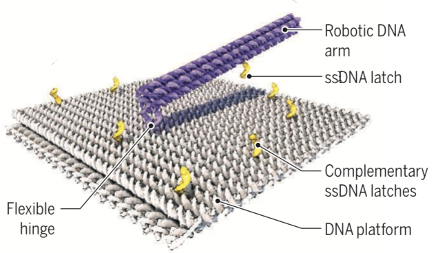
German researchers created a 55-nm-by-55-nm DNA-based molecular platform with a 25-nm-long robotic arm that can be actuated with externally applied electrical fields, under computer control. (credit: Enzo Kopperger et al./Science)

By powering a self-assembling DNA nanorobotic arm with electric fields, German scientists have achieved precise nanoscale movement that is at least five orders of magnitude (hundreds of thousands times) faster than previously reported DNA-driven robotic systems, they suggest today (Jan. 19) in the journal Science.

DNA origami has emerged as a powerful tool to build precise structures. But now, “Kopperger et al. make an impressive stride in this direction by creating a dynamic DNA origami structure that they can directly control from the macroscale with easily tunable electric fields—similar to a remote-controlled robot,” notes Björn Högberg of Karolinska Institutet in a related Perspective in Science, (p. 279).

The nanorobotic arm resembles the gearshift lever of a car. Controlled by an electric field (comparable to the car driver), short, single-stranded DNA serves as “latches” (yellow) to momentarily grab and lock the 25-nanometer-long arm into predefined “gear” positions. (credit: Enzo Kopperger et al./Science)

The new biohybrid nanorobotic systems could even act as a molecular mechanical memory (a sort of nanoscale version of the Babbage Analytical Engine), he notes. “With the capability to form long filaments with multiple DNA robot arms, the systems could also serve as a platform for new inventions in digital memory, nanoscale cargo transfer, and 3D printing of molecules.”

“The robot-arm system may be scaled up and integrated into larger hybrid systems by a combination of lithographic and self-assembly techniques,” according to the researchers. “Electrically clocked synthesis of molecules with a large number of robot arms in parallel could then be the first step toward the realization of a genuine nanorobotic production factory.”


Taking a different approach to a nanofactory, this “Productive Nanosystems: from Molecules to Superproducts” film — a collaborative project of animator and engineer John Burch and pioneer nanotechnologist K. Eric Drexler in 2005 — demonstrated key steps in a hypothetical process that converts simple molecules into a billion-CPU laptop computer. More here.


Abstract of A self-assembled nanoscale robotic arm controlled by electric fields

The use of dynamic, self-assembled DNA nanostructures in the context of nanorobotics requires fast and reliable actuation mechanisms. We therefore created a 55-nanometer–by–55-nanometer DNA-based molecular platform with an integrated robotic arm of length 25 nanometers, which can be extended to more than 400 nanometers and actuated with externally applied electrical fields. Precise, computer-controlled switching of the arm between arbitrary positions on the platform can be achieved within milliseconds, as demonstrated with single-pair Förster resonance energy transfer experiments and fluorescence microscopy. The arm can be used for electrically driven transport of molecules or nanoparticles over tens of nanometers, which is useful for the control of photonic and plasmonic processes. Application of piconewton forces by the robot arm is demonstrated in force-induced DNA duplex melting experiments.

Scientists map mammalian neural microcircuits in precise detail

Nanoengineered electroporation microelectrodes (NEMs) allow for improved current distribution and electroporation effectiveness by reducing peak voltage regions (to avoid damaging tissue). (left) Cross-section of NEM model, illustrating the total effective electroporation volume and its distribution of the voltage around the pipette tip, at a safe current of 50 microamperes. (Scale bar = 5 micrometers.) (right) A five-hole NEM after successful insertion into brain tissue, imaged with high-resolution focused ion beam (FIB). (Scale bar = 2 micrometers) (credit: D. Schwartz et al./Nature Communications)

Neuroscientists at the Francis Crick Institute have developed a new technique to map electrical microcircuits* in the brain at far more detail than existing techniques*, which are limited to tiny sections of the brain (or remain confined to simpler model organisms, like zebrafish).

In the brain, groups of neurons that connect up in microcircuits help us process information about things we see, smell and taste. Knowing how many neurons and other types of cells make up these microcircuits would give scientists a deeper understanding of how the brain computes complex information.

Nanoengineered microelectrodes

The researchers developed a new design called “nanoengineered electroporation** microelectrodes” (NEMs). They were able to use an NEM to map out all 250 cells that make up a specific microcircuit in a part of a mouse brain that processes smell (known as the “olfactory bulb glomerulus”) in a horizontal slice of the olfactory bulb — something never before achieved.

To do that, the team created a series of tiny pores (holes) near the end of a micropipette using nano-engineering tools. The new design distributes the electrical current uniformly over a wider area (up to a radius of about 50 micrometers — the size of a typical neural microcircuit), with minimal cell damage.

The researchers tested the NEM technique with a specific microcircuit, the olfactory bulb glomerulus (which detects smells). They were able to identify detailed, long-range, complex anatomical features (scale bar = 100 micrometers). (White arrows identify parallel staining of vascular structures.) (credit: D. Schwartz et al./Nature Communications)

Seeing 100% of the cells in a brain microcircuit for the first time

Unlike current methods, the team was able to stain up to 100% of the cells in the microcircuit they were investigating, according to Andreas Schaefer, who led the research, which was published in open-access Nature Communications today (Jan. 12, 2018).

“As the brain is made up of repeating units, we can learn a lot about how the brain works as a computational machine by studying it at this [microscopic] level,” he said. “Now that we have a tool of mapping these tiny units, we can start to interfere with specific cell types to see how they directly control behavior and sensory processing.”

The work was conducted in collaboration with researchers at the Max-Planck-Institute for Medical Research in Heidelberg, Heidelberg University, Heidelberg University Hospital, University College London, the MRC National Institute for Medical Research, and Columbia University Medical Center.

* Scientists currently use color-tagged viruses or charged dyes with applied electroporation current to stain brain cells. These methods, using a glass capillary with a single hole, are limited to low current (higher current could damage tissue), so they can only allow for identifying a limited area of a microcircuit.

** Electroporation is a microbiology technique that applies an electrical field to cells to increase the permeability (ease of penetration) of the cell membrane, allowing (in this case) fluorophores (fluorescent, or glowing dyes) to penetrate into the cells to label (identify parts of) the neural microcircuits (including the “inputs” and “outputs”) under a microscope.


Abstract of Architecture of a mammalian glomerular domain revealed by novel volume electroporation using nanoengineered microelectrodes

Dense microcircuit reconstruction techniques have begun to provide ultrafine insight into the architecture of small-scale networks. However, identifying the totality of cells belonging to such neuronal modules, the “inputs” and “outputs,” remains a major challenge. Here, we present the development of nanoengineered electroporation microelectrodes (NEMs) for comprehensive manipulation of a substantial volume of neuronal tissue. Combining finite element modeling and focused ion beam milling, NEMs permit substantially higher stimulation intensities compared to conventional glass capillaries, allowing for larger volumes configurable to the geometry of the target circuit. We apply NEMs to achieve near-complete labeling of the neuronal network associated with a genetically identified olfactory glomerulus. This allows us to detect sparse higher-order features of the wiring architecture that are inaccessible to statistical labeling approaches. Thus, NEM labeling provides crucial complementary information to dense circuit reconstruction techniques. Relying solely on targeting an electrode to the region of interest and passive biophysical properties largely common across cell types, this can easily be employed anywhere in the CNS.

3D-printing biocompatible living bacteria

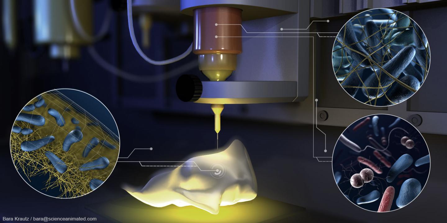
3D-printing with an ink containing living bacteria (credit: Bara Krautz/bara@scienceanimated.com)

Researchers at ETH Zurich university have developed a technique for 3D-printing biocompatible living bacteria for the first time — making it possible to produce produce high-purity cellulose for biomedical applications and nanofilters that can break down toxic substances (in drinking water, for example) or for use in disastrous oil spills, for example.

The technique, called “Flink” (“functional living ink”) allows for printing mini biochemical factories with properties that vary based on which species of bacteria are used. Up to four different inks containing different species of bacteria at different concentrations can be printed in a single pass.

Schematics of the Flink 3D bacteria-printing process for creating two types of functional living materials. (Left and center) Bacteria are embedded in a biocompatible hydrogel (which provides the supporting structure). (Right) The inclusion of P. putida* or A. xylinum* bacteria in the ink yields 3D-printed materials capable of degrading environmental pollutants (top) or forming bacterial cellulose in situ for biomedical applications (bottom), respectively. (credit: Manuel Schaffner et al./Science Advances)

The technique was described Dec. 1, 2017 in the open-access journal Science Advances.

(Left) A. xylinum bacteria were used in printing a cellulose nanofibril network (scanning electron microscope image), which was deposited (Right) on a doll face, forming a cellulose-reinforced hydrogel that, after removal of all biological residues, could serve as a skin transplant. (credit: Manuel Schaffner et al./Science Advances)

“The in situ formation of reinforcing cellulose fibers within the hydrogel is particularly attractive for regions under mechanical tension, such as the elbow and knee, or when administered as a pouch onto organs to prevent fibrosis after surgical implants and transplantations,” the researchers note in the paper. “Cellulose films grown in complex geometries precisely match the topography of the site of interest, preventing the formation of wrinkles and entrapments of contaminants that could impair the healing process. We envision that long-term medical applications will benefit from the presented multimaterial 3D printing process by locally deploying bacteria where needed.”

 * Pseudomonas putida breaks down the toxic chemical phenol, which is produced on a grand scale in the chemical industry; Acetobacter xylinum secretes high-purity nanocellulose, which relieves pain, retains moisture and is stable, opening up potential applications in the treatment of burns.


Abstract of 3D printing of bacteria into functional complex materials

Despite recent advances to control the spatial composition and dynamic functionalities of bacteria embedded in materials, bacterial localization into complex three-dimensional (3D) geometries remains a major challenge. We demonstrate a 3D printing approach to create bacteria-derived functional materials by combining the natural diverse metabolism of bacteria with the shape design freedom of additive manufacturing. To achieve this, we embedded bacteria in a biocompatible and functionalized 3D printing ink and printed two types of “living materials” capable of degrading pollutants and of producing medically relevant bacterial cellulose. With this versatile bacteria-printing platform, complex materials displaying spatially specific compositions, geometry, and properties not accessed by standard technologies can be assembled from bottom up for new biotechnological and biomedical applications.

Why (most) future robots won’t look like robots

A future robot’s body could combine soft actuators and stiff structure, with distributed computation throughout — an example of the new “material robotics.” (credit: Nikolaus Correll/University of Colorado)

Future robots won’t be limited to humanoid form (like Boston Robotics’ formidable backflipping Atlas). They’ll be invisibly embedded everywhere in common objects.

Such as a shoe that can intelligently support your gait, change stiffness as you’re running or walking, and adapt to different surfaces — or even help you do backflips.

That’s the vision of researchers at Oregon State University, the University of Colorado, Yale University, and École Polytechnique Fédérale de Lausanne, who describe the burgeoning new field of  “material robotics” in a perspective article published Nov. 29, 2017 in Science Robotics. (The article cites nine articles in this special issue, three of which you can access for free.)

Disappearing into the background of everyday life

The authors challenge a widespread basic assumption: that robots are either “machines that run bits of code” or “software ‘bots’ interacting with the world through a physical instrument.”

“We take a third path: one that imbues intelligence into the very matter of a robot,” says Oregon State University researcher Yiğit Mengüç, an assistant professor of mechanical engineering in OSU’s College of Engineering and part of the college’s Collaborative Robotics and Intelligent Systems Institute.

On that path, materials scientists are developing new bulk materials with the inherent multifunctionality required for robotic applications, while roboticists are working on new material systems with tightly integrated components, disappearing into the background of everyday life. “The spectrum of possible ap­proaches spans from soft grippers with zero knowledge and zero feedback all the way to humanoids with full knowledge and full feed­back,” the authors note in the paper.

For example, “In the future, your smartphone may be made from stretchable, foldable material so there’s no danger of it shattering,” says Mengüç. “Or it might have some actuation, where it changes shape in your hand to help with the display, or it can be able to communicate something about what you’re observing on the screen. All these bits and pieces of technology that we take for granted in life will be living, physically responsive things, moving, changing shape in response to our needs, not just flat, static screens.”

Soft robots get superpowers

Origami-inspired artificial muscles capable of lifting up to 1,000 times their own weight, simply by applying air or water pressure (credit: Shuguang Li/Wyss Institute at Harvard University)

As a good example of material-enabled robotics, researchers at the Wyss Institute at Harvard University and MIT’s Computer Science and Artificial Intelligence Laboratory (CSAIL) have developed origami-inspired, programmable, super-strong artificial muscles that will allow future soft robots to lift objects that are up to 1,000 times their own weight — using only air or water pressure.

The actuators are “programmed” by the structural design itself. The skeleton folds define how the whole structure moves — no control system required.

That allows the muscles to be very compact and simple, which makes them more appropriate for mobile or body-mounted systems that can’t accommodate large or heavy machinery, says Shuguang Li, Ph.D., a Postdoctoral Fellow at the Wyss Institute and MIT CSAIL and first author of an an open-access article on the research published Nov. 21, 2017 in Proceedings of the National Academy of Sciences (PNAS).
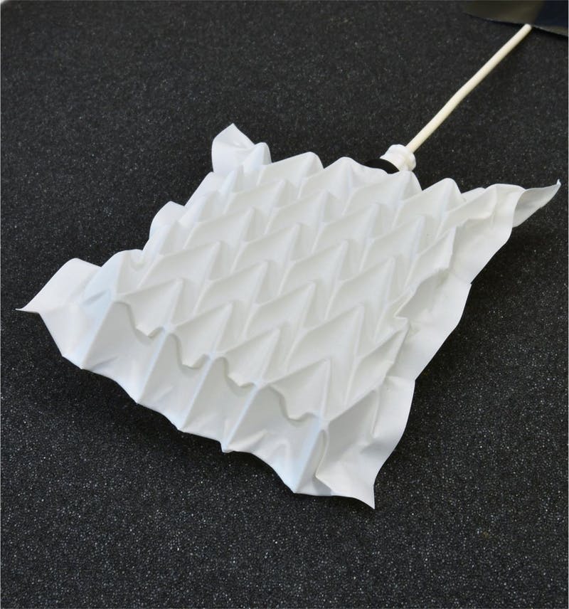
Each artificial muscle consists of an inner “skeleton” that can be made of various materials, such as a metal coil or a sheet of plastic folded into a certain pattern, surrounded by air or fluid and sealed inside a plastic or textile bag that serves as the “skin.” The structural geometry of the skeleton itself determines the muscle’s motion. A vacuum applied to the inside of the bag initiates the muscle’s movement by causing the skin to collapse onto the skeleton, creating tension that drives the motion. Incredibly, no other power source or human input is required to direct the muscle’s movement — it’s automagically determined entirely by the shape and composition of the skeleton. (credit: Shuguang Li/Wyss Institute at Harvard University)

Resilient, multipurpose, scalable

Not only can the artificial muscles move in many ways, they do so with impressive resilience. They can generate about six times more force per unit area than mammalian skeletal muscle can, and are also incredibly lightweight. A 2.6-gram muscle can lift a 3-kilogram object, which is the equivalent of a mallard duck lifting a car. Additionally, a single muscle can be constructed within ten minutes using materials that cost less than $1, making them cheap and easy to test and iterate.

These muscles can be powered by a vacuum, which makes them safer than most of the other artificial muscles currently being tested. The muscles have been built in sizes ranging from a few millimeters up to a meter. So the muscles can be used in numerous applications at multiple scales, from miniature surgical devices to wearable robotic exoskeletons, transformable architecture, and deep-sea manipulators for research or construction, up to large deployable structures for space exploration.

The team could also construct the muscles out of the water-soluble polymer PVA. That opens the possibility of bio-friendly robots that can perform tasks in natural settings with minimal environmental impact, or ingestible robots that move to the proper place in the body and then dissolve to release a drug.

The team constructed dozens of muscles using materials ranging from metal springs to packing foam to sheets of plastic, and experimented with different skeleton shapes to create muscles that can contract down to 10% of their original size, lift a delicate flower off the ground, and twist into a coil, all simply by sucking the air out of them.

This research was funded by the Defense Advanced Research Projects Agency (DARPA), the National Science Foundation (NSF), and the Wyss Institute for Biologically Inspired Engineering.


Wyss Institute | Origami-Inspired Artificial Muscles


Abstract of Fluid-driven origami-inspired artificial muscles

Artificial muscles hold promise for safe and powerful actuation for myriad common machines and robots. However, the design, fabrication, and implementation of artificial muscles are often limited by their material costs, operating principle, scalability, and single-degree-of-freedom contractile actuation motions. Here we propose an architecture for fluid-driven origami-inspired artificial muscles. This concept requires only a compressible skeleton, a flexible skin, and a fluid medium. A mechanical model is developed to explain the interaction of the three components. A fabrication method is introduced to rapidly manufacture low-cost artificial muscles using various materials and at multiple scales. The artificial muscles can be programed to achieve multiaxial motions including contraction, bending, and torsion. These motions can be aggregated into systems with multiple degrees of freedom, which are able to produce controllable motions at different rates. Our artificial muscles can be driven by fluids at negative pressures (relative to ambient). This feature makes actuation safer than most other fluidic artificial muscles that operate with positive pressures. Experiments reveal that these muscles can contract over 90% of their initial lengths, generate stresses of ∼600 kPa, and produce peak power densities over 2 kW/kg—all equal to, or in excess of, natural muscle. This architecture for artificial muscles opens the door to rapid design and low-cost fabrication of actuation systems for numerous applications at multiple scales, ranging from miniature medical devices to wearable robotic exoskeletons to large deployable structures for space exploration.
New nanomaterial, quantum encryption system could be ultimate defenses against hackers

New physically unclonable nanomaterial (credit: Abdullah Alharbi et al./ACS Nano)

Recent advances in quantum computers may soon give hackers access to machines powerful enough to crack even the toughest of standard internet security codes. With these codes broken, all of our online data — from medical records to bank transactions — could be vulnerable to attack.

Now, a new low-cost nanomaterial developed by New York University Tandon School of Engineering researchers can be tuned to act as a secure authentication key to encrypt computer hardware and data. The layered molybdenum disulfide (MoS2) nanomaterial cannot be physically cloned (duplicated) — replacing programming, which can be hacked.

In a paper published in the journal ACS Nano, the researchers explain that the new nanomaterial has the highest possible level of structural randomness, making it physically unclonable. It achieves this with randomly occurring regions that alternately emit or do not emit light. When exposed to light, this pattern can be used to create a one-of-a-kind binary cryptographic authentication key that could secure hardware components at minimal cost.

The research team envisions a future in which similar nanomaterials can be inexpensively produced at scale and applied to a chip or other hardware component. “No metal contacts are required, and production could take place independently of the chip fabrication process,” according to Davood Shahrjerdi, Assistant Professor of Electrical and Computer Engineering. “It’s maximum security with minimal investment.”

The National Science Foundation and the U.S. Army Research Office supported the research.

A high-speed quantum encryption system to secure the future internet

Schematic of the experimental quantum key distribution setup (credit: Nurul T. Islam et al./Science Advances)

Another approach to the hacker threat is being developed by scientists at Duke University, The Ohio State University and Oak Ridge National Laboratory. It would use the properties that drive quantum computers to create theoretically hack-proof forms of quantum data encryption.

Called quantum key distribution (QKD), it takes advantage of one of the fundamental properties of quantum mechanics: Measuring tiny bits of matter like electrons or photons automatically changes their properties, which would immediately alert both parties to the existence of a security breach. However, current QKD systems can only transmit keys at relatively low rates — up to hundreds of kilobits per second — which are too slow for most practical uses on the internet.

The new experimental QKD system is capable of creating and distributing encryption codes at megabit-per-second rates — five to 10 times faster than existing methods and on a par with current internet speeds when running several systems in parallel. In an online open-access article in Science Advances, the researchers show that the technique is secure from common attacks, even in the face of equipment flaws that could open up leaks.

This research was supported by the Office of Naval Research, the Defense Advanced Research Projects Agency, and Oak Ridge National Laboratory.


Abstract of Physically Unclonable Cryptographic Primitives by Chemical Vapor Deposition of Layered MoS2

Physically unclonable cryptographic primitives are promising for securing the rapidly growing number of electronic devices. Here, we introduce physically unclonable primitives from layered molybdenum disulfide (MoS2) by leveraging the natural randomness of their island growth during chemical vapor deposition (CVD). We synthesize a MoS2 monolayer film covered with speckles of multilayer islands, where the growth process is engineered for an optimal speckle density. Using the Clark–Evans test, we confirm that the distribution of islands on the film exhibits complete spatial randomness, hence indicating the growth of multilayer speckles is a spatial Poisson process. Such a property is highly desirable for constructing unpredictable cryptographic primitives. The security primitive is an array of 2048 pixels fabricated from this film. The complex structure of the pixels makes the physical duplication of the array impossible (i.e., physically unclonable). A unique optical response is generated by applying an optical stimulus to the structure. The basis for this unique response is the dependence of the photoemission on the number of MoS2 layers, which by design is random throughout the film. Using a threshold value for the photoemission, we convert the optical response into binary cryptographic keys. We show that the proper selection of this threshold is crucial for maximizing combination randomness and that the optimal value of the threshold is linked directly to the growth process. This study reveals an opportunity for generating robust and versatile security primitives from layered transition metal dichalcogenides.


Abstract of Provably secure and high-rate quantum key distribution with time-bin qudits

The security of conventional cryptography systems is threatened in the forthcoming era of quantum computers. Quantum key distribution (QKD) features fundamentally proven security and offers a promising option for quantum-proof cryptography solution. Although prototype QKD systems over optical fiber have been demonstrated over the years, the key generation rates remain several orders of magnitude lower than current classical communication systems. In an effort toward a commercially viable QKD system with improved key generation rates, we developed a discrete-variable QKD system based on time-bin quantum photonic states that can generate provably secure cryptographic keys at megabit-per-second rates over metropolitan distances. We use high-dimensional quantum states that transmit more than one secret bit per received photon, alleviating detector saturation effects in the superconducting nanowire single-photon detectors used in our system that feature very high detection efficiency (of more than 70%) and low timing jitter (of less than 40 ps). Our system is constructed using commercial off-the-shelf components, and the adopted protocol can be readily extended to free-space quantum channels. The security analysis adopted to distill the keys ensures that the demonstrated protocol is robust against coherent attacks, finite-size effects, and a broad class of experimental imperfections identified in our system.

Using microrobots to diagnose and treat illness in remote areas of the body

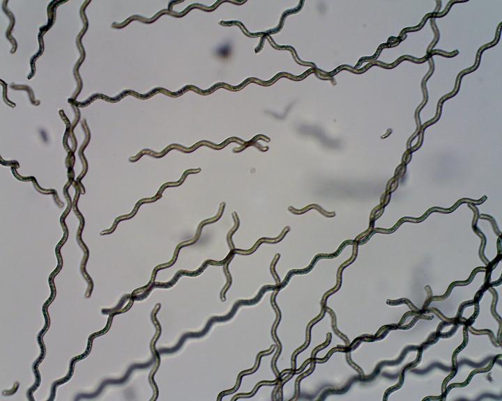
Spirulina algae coated with magnetic particles to form a microrobot. Devices such as these could be developed to diagnose and treat illness in hard-to-reach parts of the body. (credit: Yan et al./Science Robotics)

Imagine a swarm of remote-controlled microrobots, a few micrometers in length (blood-vessel-sized), unleashed into your body to swim through your intestinal track or blood vessels, for example. Goal: to diagnose illness and treat it in hard-to-reach areas of the body.

An international team of researchers, led by the Chinese University of Hong Kong, is now experimenting with this idea (starting with rats) — using microscopic Spirulina algae coated with biocompatible magnetic nanoparticles to form the microswimmers.

Schematic of dip-coating S. platensis algae in a suspension of magnetite nanoparticles and growing microrobots. The time taken for the robots to function and biodegrade within the body could be tailored by adjusting the thickness of the coating. (credit: Xiaohui Yan et al./Science Robotics)

There are two methods being studied: (1) track the microswimmers in tissue close to the skin’s surface by imaging the algae’s natural luminescence; and (2) track them in hard-to-reach deeper tissue by coating with magnetite (Fe3O4) to make them detectable with magnetic resonance imaging (MRI). The devices could also sense chemical changes linked to the onset of illness.

In lab tests, during degradation, the microswimmers were able to release potent compounds from the algae core that selectively attacked cancer cells while leaving healthy cells unharmed. Further research could show whether this might have potential as a treatment, the researchers say.

The study, published in an open-access paper in Science Robotics, was carried out in collaboration with the Universities of Edinburgh and Manchester and was supported by the Research Grants Council of Hong Kong.


Abstract of Multifunctional biohybrid magnetite microrobots for imaging-guided therapy

Magnetic microrobots and nanorobots can be remotely controlled to propel in complex biological fluids with high precision by using magnetic fields. Their potential for controlled navigation in hard-to-reach cavities of the human body makes them promising miniaturized robotic tools to diagnose and treat diseases in a minimally invasive manner. However, critical issues, such as motion tracking, biocompatibility, biodegradation, and diagnostic/therapeutic effects, need to be resolved to allow preclinical in vivo development and clinical trials. We report biohybrid magnetic robots endowed with multifunctional capabilities by integrating desired structural and functional attributes from a biological matrix and an engineered coating. Helical microswimmers were fabricated from Spirulinamicroalgae via a facile dip-coating process in magnetite (Fe3O4) suspensions, superparamagnetic, and equipped with robust navigation capability in various biofluids. The innate properties of the microalgae allowed in vivo fluorescence imaging and remote diagnostic sensing without the need for any surface modification. Furthermore, in vivo magnetic resonance imaging tracked a swarm of microswimmers inside rodent stomachs, a deep organ where fluorescence-based imaging ceased to work because of its penetration limitation. Meanwhile, the microswimmers were able to degrade and exhibited selective cytotoxicity to cancer cell lines, subject to the thickness of the Fe3O4 coating, which could be tailored via the dip-coating process. The biohybrid microrobots reported herein represent a microrobotic platform that could be further developed for in vivo imaging–guided therapy and a proof of concept for the engineering of multifunctional microrobotic and nanorobotic devices.

Fast-moving spinning magnetized nanoparticles could lead to ultra-high-speed, high-density data storage

Artist’s impression of skyrmion data storage (credit: Moritz Eisebitt)

An international team led by MIT associate professor of materials science and engineering Geoffrey Beach has demonstrated a practical way to use “skyrmions” to create a radical new high-speed, high-density data-storage method that could one day replace disk drives — and even replace high-speed RAM memory.

Rather than reading and writing data one bit at a time by changing the orientation of magnetized nanoparticles on a surface, Skyrmions could store data using only a tiny area of a magnetic surface — perhaps just a few atoms across — and for long periods of time, without the need for further energy input (unlike disk drives and RAM).

Beach and associates conceive skyrmions as little sub-nanosecond spin-generating eddies of magnetism controlled by electric fields — replacing the magnetic-disk system of reading and writing data one bit at a time. In experiments, skyrmions have been generated on a thin metallic film sandwiched with non-magnetic heavy metals and transition-metal ferromagnetic layers — exploiting a defect, such as a constriction in the magnetic track.*

Skyrmions are also highly stable to external magnetic and mechanical perturbations, unlike the individual magnetic poles in a conventional magnetic storage device — allowing for vastly more data to be written onto a surface of a given size.

A practical data-storage system

Google data center (credit: Google Inc.)

Beach has recently collaborated with researchers at MIT and others in Germany** to demonstrate experimentally for the first time that it’s possible to create skyrmions in specific locations, which is needed for a data-storage system. The new findings were reported October 2, 2017 in the journal Nature Nanotechnology.

Conventional magnetic systems are now reaching speed and density limits set by the basic physics of their existing materials. The new system, once perfected, could provide a way to continue that progress toward ever-denser data storage, Beach says.

However, the researchers note that to create a commercialized system will require an efficient, reliable way to create skyrmions when and where they were needed, along with a way to read out the data (which now requires sophisticated, expensive X-ray magnetic spectroscopy). The team is now pursuing possible strategies to accomplish that.***

* The system focuses on the boundary region between atoms whose magnetic poles are pointing in one direction and those with poles pointing the other way. This boundary region can move back and forth within the magnetic material, Beach says. What he and his team found four years ago was that these boundary regions could be controlled by placing a second sheet of nonmagnetic heavy metal very close to the magnetic layer. The nonmagnetic layer can then influence the magnetic one, with electric fields in the nonmagnetic layer pushing around the magnetic domains in the magnetic layer. Skyrmions are little swirls of magnetic orientation within these layers. The key to being able to create skyrmions at will in particular locations lays in material defects. By introducing a particular kind of defect in the magnetic layer, the skyrmions become pinned to specific locations on the surface, the team found. Those surfaces with intentional defects can then be used as a controllable writing surface for data encoded in the skyrmions.

** The team also includes researchers at the Max Born Institute and the Institute of Optics and Atomic Physics, both in Berlin; the Institute for Laser Technologies in Medicine and Metrology at the University of Ulm, in Germany; and the Deutches Elektroniken-Syncrotron (DESY), in Hamburg. The work was supported by the U.S. Department of Energy and the German Science Foundation.

*** The researchers believe an alternative way of reading the data is possible, using an additional metal layer added to the other layers. By creating a particular texture on this added layer, it may be possible to detect differences in the layer’s electrical resistance depending on whether a skyrmion is present or not in the adjacent layer.


Abstract of Field-free deterministic ultrafast creation of magnetic skyrmions by spin–orbit torques

Magnetic skyrmions are stabilized by a combination of external magnetic fields, stray field energies, higher-order exchange interactions and the Dzyaloshinskii–Moriya interaction (DMI). The last favours homochiral skyrmions, whose motion is driven by spin–orbit torques and is deterministic, which makes systems with a large DMI relevant for applications. Asymmetric multilayers of non-magnetic heavy metals with strong spin–orbit interactions and transition-metal ferromagnetic layers provide a large and tunable DMI. Also, the non-magnetic heavy metal layer can inject a vertical spin current with transverse spin polarization into the ferromagnetic layer via the spin Hall effect. This leads to torques that can be used to switch the magnetization completely in out-of-plane magnetized ferromagnetic elements, but the switching is deterministic only in the presence of a symmetry-breaking in-plane field. Although spin–orbit torques led to domain nucleation in continuous films and to stochastic nucleation of skyrmions in magnetic tracks, no practical means to create individual skyrmions controllably in an integrated device design at a selected position has been reported yet. Here we demonstrate that sub-nanosecond spin–orbit torque pulses can generate single skyrmions at custom-defined positions in a magnetic racetrack deterministically using the same current path as used for the shifting operation. The effect of the DMI implies that no external in-plane magnetic fields are needed for this aim. This implementation exploits a defect, such as a constriction in the magnetic track, that can serve as a skyrmion generator. The concept is applicable to any track geometry, including three-dimensional designs.

New transistor design enables flexible, high-performance wearable/mobile electronics

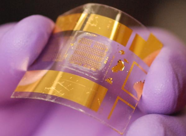
Advanced flexible transistor developed at UW-Madison (photo credit: Jung-Hun Seo/University at Buffalo, State University of New York)

A team of University of Wisconsin–Madison (UW–Madison) engineers has created “the most functional flexible transistor in the world,” along with a fast, simple, inexpensive fabrication process that’s easily scalable to the commercial level.

The development promises to allow manufacturers to add advanced, smart-wireless capabilities to wearable and mobile devices that curve, bend, stretch and move.*

The UW–Madison group’s advance is based on a BiCMOS (bipolar complementary metal oxide semiconductor) thin-film transistor, combining speed, high current, and low power dissipation (heat and wasted energy) on just one surface (a silicon nanomembrane, or “Si NM”).**

BiCMOS transistors are the chip of choice for “mixed-signal” devices (combining analog and digital capabilities), which include many of today’s portable electronic devices such as cellphones. “The [BiCMOS] industry standard is very good,” says Zhenqiang (Jack) Ma, the Lynn H. Matthias Professor and Vilas Distinguished Achievement Professor in electrical and computer engineering at UW–Madison. “Now we can do the same things with our transistor — but it can bend.”

The research was described in the inaugural issue of Nature Publishing Group’s open-access journal Flexible Electronics, published Sept. 27, 2017.***

Making traditional BiCMOS flexible electronics is difficult, in part because the process takes several months and requires a multitude of delicate, high-temperature steps. Even a minor variation in temperature at any point could ruin all of the previous steps.

Ma and his collaborators fabricated their flexible electronics on a single-crystal silicon nanomembrane on a single bendable piece of plastic. The secret to their success is their unique process, which eliminates many steps and slashes both the time and cost of fabricating the transistors.

“In industry, they need to finish these in three months,” he says. “We finished it in a week.”

He says his group’s much simpler, high-temperature process can scale to industry-level production right away.

“The key is that parameters are important,” he says. “One high-temperature step fixes everything — like glue. Now, we have more powerful mixed-signal tools. Basically, the idea is for [the flexible electronics platform] to expand with this.”

* Some companies (such as Samsung) have developed flexible displays, but not other flexible electronic components in their devices, Ma explained to KurzweilAI.

** “Flexible electronics have mainly focused on their form factors such as bendability, lightweight, and large area with low-cost processability…. To date, all the [silicon, or Si]-based thin-film transistors (TFTs) have been realized with CMOS technology because of their simple structure and process. However, as more functions are required in future flexible electronic applications (i.e., advanced bioelectronic systems or flexible wireless power applications), an integration of functional devices in one flexible substrate is needed to handle complex signals and/or various power levels.” — Jung Hun Seo et al./Flexible Electronics. The n-channel, p-channel metal-oxide semiconductor field-effect transistors (N-MOSFETs & P-MOSFETs), and NPN bipolar junction transistors (BJTs) were realized together on a 340-nm thick Si NM layer. 

*** Co-authors included researchers at the University at Buffalo, State University of New York, and the University of Texas at Arlington. This work was supported by the Air Force Office Of Scientific Research.


Abstract of High-performance flexible BiCMOS electronics based on single-crystal Si nanomembrane

In this work, we have demonstrated for the first time integrated flexible bipolar-complementary metal-oxide-semiconductor (BiCMOS) thin-film transistors (TFTs) based on a transferable single crystalline Si nanomembrane (Si NM) on a single piece of bendable plastic substrate. The n-channel, p-channel metal-oxide semiconductor field-effect transistors (N-MOSFETs & P-MOSFETs), and NPN bipolar junction transistors (BJTs) were realized together on a 340-nm thick Si NM layer with minimized processing complexity at low cost for advanced flexible electronic applications. The fabrication process was simplified by thoughtfully arranging the sequence of necessary ion implantation steps with carefully selected energies, doses and anneal conditions, and by wisely combining some costly processing steps that are otherwise separately needed for all three types of transistors. All types of TFTs demonstrated excellent DC and radio-frequency (RF) characteristics and exhibited stable transconductance and current gain under bending conditions. Overall, Si NM-based flexible BiCMOS TFTs offer great promises for high-performance and multi-functional future flexible electronics applications and is expected to provide a much larger and more versatile platform to address a broader range of applications. Moreover, the flexible BiCMOS process proposed and demonstrated here is compatible with commercial microfabrication technology, making its adaptation to future commercial use straightforward.

Ray Kurzweil on The Age of Spiritual Machines: A 1999 TV interview

Dear readers,

For your interest, this 1999 interview with me, which I recently re-watched, describes some interesting predictions that are still coming true today. It’s intriguing to look back at the last 18 years to see what actually unfolded. This video is a compelling glimpse into the future, as we’re living it today.

Enjoy!

— Ray


Dear readers,

This interview by Harold Hudson Channer was recorded on Jan. 14, 1999 and aired February 1, 1999 on a Manhattan Neighborhood Network cable-access show, Conversations with Harold Hudson Channer.

In the discussion, Ray explains many of the ahead-of-their-time ideas presented in The Age of Spiritual Machines*, such as the “law of accelerating returns” (how technological change is exponential, contrary to the common-sense “intuitive linear” view); the forthcoming revolutionary impacts of AI; nanotech brain and body implants for increased intelligence, improved health, and life extension; and technological impacts on economic growth.

I was personally inspired by the book in 1999 and by Ray’s prophetic, uplifting vision of the future. I hope you also enjoy this blast from the past.

— Amara D. Angelica, Editor

* First published in hardcover January 1, 1999 by Viking. The series also includes The Age of Intelligent Machines (The MIT Press, 1992) and The Singularity Is Near (Penquin Books, 2006).

Walking DNA nanorobot could deliver a drug to a precise location in your body

DNA nanorobot cargo carrier (artist’s impression) (credit: Ella Maru Studio)

Caltech scientists have developed a “cargo sorting” DNA nanorobot programmed to autonomously “walk” around a surface, pick up certain molecules, and drop them off in designated locations.

The research is described in a paper in the Friday, September 15, 2017 issue of Science.

The major advance in this study is “their methodology for designing simple DNA devices that work in parallel to solve nontrivial tasks,” notes Duke University computer scientist John H. Reif in an article in the same issue of Science.

Such tasks could include synthesizing a drug in a molecular factory or delivering a drug only when a specific signal is present in bloodstreams, say the researchers. “So far, the development of DNA robots has been limited to simple functions,” the researchers note.

Walking nanobots that work in parallel

Conceptual illustration of two DNA nanorobots collectively performing a cargo-sorting task on a DNA origami surface: transporting fluorescent molecules with different colors from initially random locations to ordered destinations. (credit: Demin Liu)

The DNA nanorobot, intended as a proof of concept, has a “leg” with two “feet” for walking, and an “arm” and “hand” for picking up cargo. It also has a segment that can recognize a specific drop-off point and signal to the hand to release its cargo. Each of these building blocks are made of just a few nucleotides (molecules that form DNA) within a single strand of DNA.*

As the robot encounters cargo molecules tethered to pegs, it grabs them with its “hand” components and carries them around (with a 6-nm step size) until it detects the signal of the drop-off point.

Multiple DNA nanorobots independently execute three operations in parallel: [1] cargo pickup, [2] random movement to adjacent stepping stones, and [3] cargo drop-off at ordered locations. (credit: C. Bickel/Science)

In experiments, the nanorobots successfully sorted six randomly scattered molecules into their correct places in 24 hours. The process is slow, but adding more robots to the surface shortened the time it took to complete the task. The very simple robot design utilizes very little chemical energy, according to the researchers.**

“The same system design can be generalized to work with dozens of types of cargos at any arbitrary initial location on the surface,” says lead author Anupama Thubagere. “One could also have multiple robots performing diverse sorting tasks in parallel,” [programmed] like macroscopic robots.”

Future applications

“We don’t develop DNA robots for any specific applications. Our lab focuses on discovering the engineering principles that enable the development of general-purpose DNA robots,” explains Lulu Qian, assistant professor of bioengineering.

“However, it is my hope that other researchers could use these principles for exciting applications, such as synthesizing a therapeutic chemical from its constituent parts in an artificial molecular factory, or sorting molecular components in trash for recycling. Just like electromechanical robots are sent off to faraway places, like Mars, we would like to send molecular robots to minuscule places where humans can’t go, such as the bloodstream.”

Funding was provided by Caltech Summer Undergraduate Research Fellowships, the National Science Foundation, and the Burroughs Wellcome Fund.

* The key to designing DNA machines is the fact that DNA has unique chemical and physical properties that are known and programmable. A single strand of DNA is made up of four different molecules called nucleotides—abbreviated A, G, C, and T—and arranged in a string called a sequence. These nucleotides bond in specific pairs: A with T, and G with C. When a single strand encounters a “reverse complementary strand” — for example, CGATT meets AATCG —the two strands zip together in the classic double-helix shape.

** Using these chemical and physical principles, researchers can also design “playgrounds,” such as molecular pegboards, to test them on, according to the researchers. In the current work, the DNA robot moves around on a 58-nanometer-by-58-nanometer pegboard on which the pegs are made of single strands of DNA complementary to the robot’s leg and foot. The robot binds to a peg with its leg and one of its feet — the other foot floats freely. When random molecular fluctuations cause this free foot to encounter a nearby peg, it pulls the robot to the new peg and its other foot is freed. This process continues with the robot moving in a random direction at each step.


Abstract of A cargo-sorting DNA robot

Two critical challenges in the design and synthesis of molecular robots are modularity and
algorithm simplicity.We demonstrate three modular building blocks for a DNA robot that
performs cargo sorting at themolecular level. A simple algorithm encoding recognition between
cargos and their destinations allows for a simple robot design: a single-stranded DNA with
one leg and two foot domains for walking, and one arm and one hand domain for picking up and
dropping off cargos.The robot explores a two-dimensional testing ground on the surface of
DNA origami, picks up multiple cargos of two types that are initially at unordered locations, and
delivers them to specified destinations until all molecules are sorted into two distinct piles.
The robot is designed to perform a random walk without any energy supply. Exploiting this
feature, a single robot can repeatedly sort multiple cargos. Localization on DNA origami allows
for distinct cargo-sorting tasks to take place simultaneously in one test tube or for multiple
robots to collectively perform the same task.