‘I’ve seen the future, and it’s …. paper’

Interlocking origami zigzag paper tubes can be configured to build a variety of structures that have stiffness and function, but can fold compactly for storage or shipping. (credit: Rob Felt)

A new origami “zippered tube” design that makes paper-based (or other thin materials) structures stiff enough to hold weight, yet can fold flat for easy shipping and storage could transform structures ranging from microscopic robots to furniture and even buildings.

That’s what researchers from the University of Illinois at Urbana-Champaign, the Georgia Institute of Technology, and the University of Tokyo suggest in a Proceedings of the National Academy of Sciences paper.

Such origami structures could include a robotic arm that reaches out and scrunches up, a construction crane that folds to pick up or deliver a load,  furniture, and quick-assembling emergency shelters, bridges — and other infrastructure used in the wake of a natural disaster.

Pop-up buildings?

The researchers use a particular origami technique called Miura-ori folding: They make precise, zigzag-folded strips of paper, then glue two strips together to make a tube. While the single strip of paper is highly flexible, the tube is stiffer and does not fold in as many directions.

Interlocking two tubes in zipper-like fashion made them much stiffer and harder to twist or bend, they found. The structure folds up flat, yet rapidly and easily expands to the rigid tube configuration.

The zipper configuration works even with tubes that have different angles of folding. By combining tubes with different geometries, the researchers can make many different three-dimensional structures, such as a bridge, a canopy, or a tower.
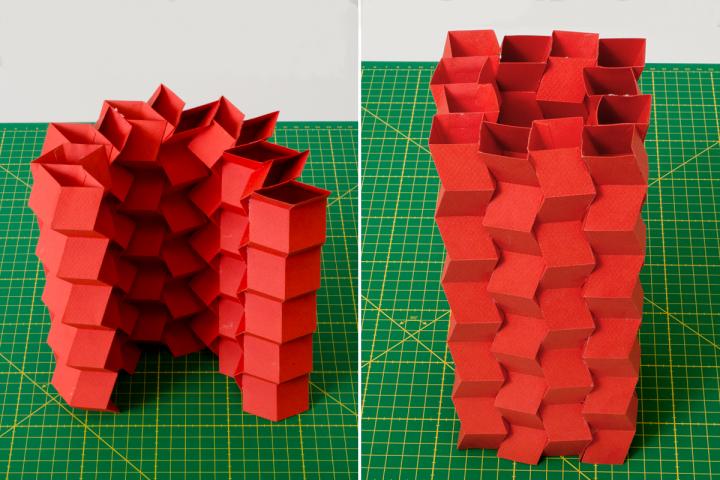
Origami “zipper tubes” — interlocking zigzag paper tubes — can be configured to build a variety of structures that have stiffness and function, but can fold compactly for storage or shipping (credit: L. Brian Stauffer)

Transformable structures

“The ability to change functionality in real time is a real advantage in origami,” said Georgia Tech professor Glaucio Paulino. “By having these transformable structures, you can change their functionality and make them adaptable. They are reconfigurable. You can change the material characteristics: You can make them stiffer or softer depending on the intended use.”

The team uses paper prototypes to demonstrate how a thin, flexible sheet can be folded into functional structures, but their techniques could be applied to other thin materials, according to the researchers. Larger-scale applications could combine metal or plastic panels with hinges.

Next, the researchers plan to explore new combinations of tubes with different folding angles to build new structures. They also hope to apply their techniques to other materials and explore applications from large-scale construction to microscopic structures for biomedical devices or robotics.

“All of these ideas apply from the nanoscale and microscale up to large scales and even structures that NASA would deploy into space,” Paulino said. “Depending on your interest, the applications are endless. We have just scratched the surface. Once you have a powerful concept, which we think the zipper coupling is, you can explore applications in many different areas.”


Abstract of Origami tubes assembled into stiff, yet reconfigurable structures and metamaterials

Thin sheets have long been known to experience an increase in stiffness when they are bent, buckled, or assembled into smaller interlocking structures. We introduce a unique orientation for coupling rigidly foldable origami tubes in a “zipper” fashion that substantially increases the system stiffness and permits only one flexible deformation mode through which the structure can deploy. The flexible deployment of the tubular structures is permitted by localized bending of the origami along prescribed fold lines. All other deformation modes, such as global bending and twisting of the structural system, are substantially stiffer because the tubular assemblages are overconstrained and the thin sheets become engaged in tension and compression. The zipper-coupled tubes yield an unusually large eigenvalue bandgap that represents the unique difference in stiffness between deformation modes. Furthermore, we couple compatible origami tubes into a variety of cellular assemblages that can enhance mechanical characteristics and geometric versatility, leading to a potential design paradigm for structures and metamaterials that can be deployed, stiffened, and tuned. The enhanced mechanical properties, versatility, and adaptivity of these thin sheet systems can provide practical solutions of varying geometric scales in science and engineering.

Lipid DNA origami may lead to advanced future nanomachines

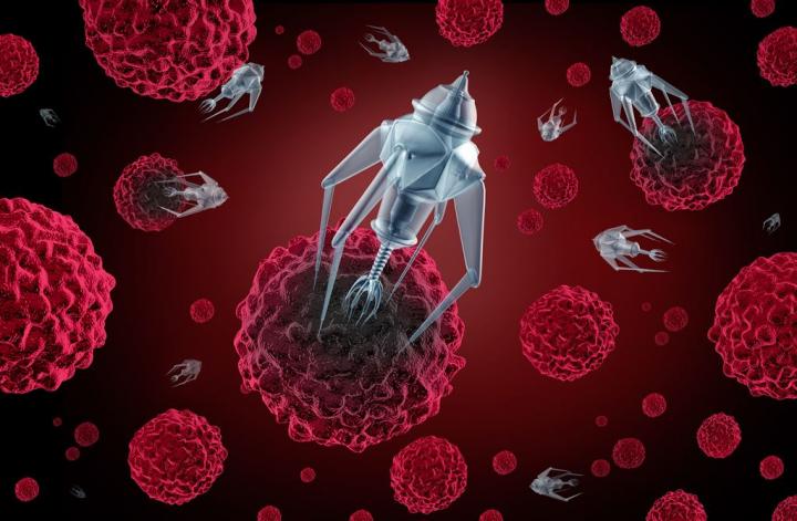
Using a double layer of lipids facilitates assembly of DNA origami nanostructures, bringing us one step closer to future DNA nanomachines, as in this artist’s impression (credit: Kyoto University’s Institute for Integrated Cell-Material Sciences)

Kyoto University scientists in Japan have developed a method for creating larger 2-D self-assembling DNA origami* nanostructures.

Current DNA origami methods can create extremely small two- and three-dimensional shapes that could be used as construction material to build nanodevices, such as nanomotors, in the future for targeted drug delivery inside the body, for example. KurzweilAI recently covered advanced methods developed by Brookhaven National Laboratory and  Arizona State University’s Biodesign Institute.

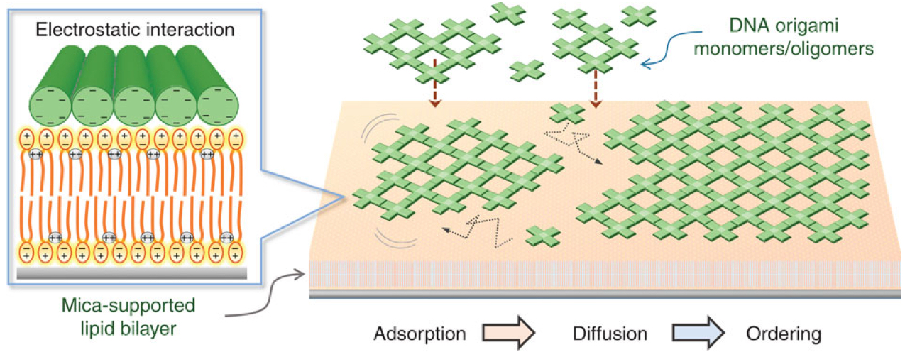
Lipid bilayer allows DNA origami structures to easily self-assemble into 2-D nanostructures (credit: Yuki Suzuki et al./Nature Communications)

Unlike those rigid structures, the Kyoto scientists used a double layer of lipids (fats) containing both a positive and a negative charge. That caused the DNA origami structures to be absorbed onto the lipid layer via electrostatic interaction. The weak bond between the origami structures and the lipid layer allowed them to move more freely than in other approaches, facilitating their interaction with one another and allowing them to self-assemble and form larger structures.

“We anticipate that our approach will further expand the potential applications of DNA origami structures and their assemblies in the fields of nanotechnology, biophysics, and synthetic biology,” says chemical biologist Professor Hiroshi Sugiyama from Kyoto University’s Institute for Integrated Cell-Material Sciences (iCeMS).

The study was published in an open-access paper in Nature Communications on August 27, 2015.

* The technique of DNA origami capitalizes on the simple base-pairing properties of DNA, a molecule built from the four nucleotides Adenine (A)Thymine (T)Cytosine (C) and Guanine (G). The rules of the game are simple: A’s always pair with T’s and C’s with G’s. Using this abbreviated vocabulary, the myriad body plans of all living organisms are constructed; though duplicating even Nature’s simpler designs has required great ingenuity.

The basic idea of DNA origami is to use a length of single-stranded DNA as a scaffold for the desired shape. Base-pairing of complementary nucleotides causes the form to fold and self-assemble. The process is guided by the addition of shorter “staple strands,” which act to help fold the scaffold and to hold the resulting structure together. Various imaging technologies are used to observe the tiny structures, including fluorescence-, electron- and atomic-force microscopy.


Abstract of Lipid-bilayer-assisted two-dimensional self-assembly of DNA origami nanostructures

Self-assembly is a ubiquitous approach to the design and fabrication of novel supermolecular architectures. Here we report a strategy termed ‘lipid-bilayer-assisted self-assembly’ that is used to assemble DNA origami nanostructures into two-dimensional lattices. DNA origami structures are electrostatically adsorbed onto a mica-supported zwitterionic lipid bilayer in the presence of divalent cations. We demonstrate that the bilayer-adsorbed origami units are mobile on the surface and self-assembled into large micrometre-sized lattices in their lateral dimensions. Using high-speed atomic force microscopy imaging, a variety of dynamic processes involved in the formation of the lattice, such as fusion, reorganization and defect filling, are successfully visualized. The surface modifiability of the assembled lattice is also demonstrated by in situ decoration with streptavidin molecules. Our approach provides a new strategy for preparing versatile scaffolds for nanofabrication and paves the way for organizing functional nanodevices in a micrometer space.

Carbon dioxide capture by a novel material that mimics a plant enzyme

Atomic structure of the adsorbed* carbon dioxide (gray sphere bonded to two red spheres) inserted between the manganese (green sphere) and amine (blue sphere) groups within the novel metal-organic framework, forming a linear chain of ammonium carbamate (top). Some hydrogen atoms (white sphere) are omitted for clarity. (credit: Image courtesy of Thomas McDonald, Jarad Mason, and Jeffrey Long)

A novel porous material that achieves carbon dioxide (CO2) capture-and-release with only small shifts in temperature has been developed by a team of researchers at the Center for Gas Separations Relevant to Clean Energy Technologies, led by the University of California, Berkeley (a DOE Energy Frontier Research Center), and associates.

This metal-organic framework (MOF) structure, which adsorbs* CO2, closely resembles an enzyme found in plants known as RuBisCO, which captures CO2 from the atmosphere for conversion into nutrients.

The discovery* paves the way for designing more efficient materials that dramatically reduce overall energy cost of carbon capture. Such materials could be used for carbon capture from fossil-fuel-based power plants as well as from the atmosphere, mitigating the greenhouse effect.

The enhanced carbon capture efficiency of the new class of materials could allow for dramatic reductions in the overall energy cost of carbon capture in power plants or even from the atmosphere, according to the researchers.

* Adsorbed CO2 is captured on the surface of a material; absorbed CO2 is captured inside the material.

** The cooperative mechanism for carbon dioxide (CO2) adsorption in porous MOF materials:

First, a CO2 molecule gets inserted between a metal ion and an amine group within the cylindrical pore of the MOF. Interestingly, the chemical environment of the MOF with the adsorbed CO2  is very similar to that of plant enzyme RuBisCO with a bound CO2.

RuBisCO plays an essential role in biological carbon fixation by plants and conversion into nutrients. In the case of the newly synthesized diamine-appended MOFs, however, the inserted CO2 reorganizes the chemical environment at the adjacent metal ion site to be just right for the insertion of the next CO2.

As more CO2 enters the pore, a cooperative domino effect ensues that leads to the formation of linear chains of ammonium carbamate along the cylindrical pore surfaces of the MOF.

Gas adsorption measurements show the high selectivity of the material for CO2 from the typical composition of flue gas from fossil-fuel-based power plants that contains nitrogen, water, and CO2.

Furthermore, the material has large working capacities — the amount of CO2 adsorbed and desorbed for a given amount of material — that are enabled by only moderate temperature shifts for the adsorption and desorption processes.

Finally, the research points out that changing the strength of the metal-diamine bond through metal substitution allows for rational tuning of the adsorption and desorption properties.


Abstract of Cooperative insertion of CO2 in diamine-appended metal-organic frameworks

The process of carbon capture and sequestration has been proposed as a method of mitigating the build-up of greenhouse gases in the atmosphere. If implemented, the cost of electricity generated by a fossil fuel-burning power plant would rise substantially, owing to the expense of removing CO2 from the effluent stream. There is therefore an urgent need for more efficient gas separation technologies, such as those potentially offered by advanced solid adsorbents. Here we show that diamine-appended metal-organic frameworks can behave as ‘phase-change’ adsorbents, with unusual step-shaped CO2 adsorption isotherms that shift markedly with temperature. Results from spectroscopic, diffraction and computational studies show that the origin of the sharp adsorption step is an unprecedented cooperative process in which, above a metal-dependent threshold pressure, CO2 molecules insert into metal-amine bonds, inducing a reorganization of the amines into well-ordered chains of ammonium carbamate. As a consequence, large CO2 separation capacities can be achieved with small temperature swings, and regeneration energies appreciably lower than achievable with state-of-the-art aqueous amine solutions become feasible. The results provide a mechanistic framework for designing highly efficient adsorbents for removing CO2 from various gas mixtures, and yield insights into the conservation of Mg2+ within the ribulose-1,5-bisphosphate carboxylase/oxygenase family of enzymes.

Silk bio-ink could help advance tissue engineering using 3-D printers

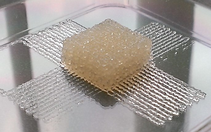
Scientists have developed a silk-based, 3-D printer ink for use in biomedical implants or tissue engineering (credit: American Chemical Society )

Tufts University scientists have developed a silk-based bio-ink that could allow for printing tissues that could be loaded with pharmaceuticals, cytokines (for directing stem cell functions), and antibiotics (for controlling infections), for example, or used in biomedical implants and tissue engineering.

Current 3-D printing processes are limited to simple body parts such as bone. And most inks currently being developed for 3-D printing are made of thermoplastics, silicones, collagen, gelatin, or alginate, which have limits. For example, the temperatures, pH changes and crosslinking methods that may be required to toughen some of these materials can damage cells or other biological components that researchers would want to add to the inks.

To address these bio-ink limitations, Tufts Stern Family Professor of Engineering David L. Kaplan and associates combined silk proteins, which are biocompatible, and glycerol, a non-toxic sugar alcohol commonly found in food and pharmaceutical products. The resulting ink was clear, flexible, stable in water, and didn’t require any processing methods, such as high temperatures, that would limit its versatility.

The researchers reported their research findings in the journal ACS Biomaterials Science & Engineering.

(a−e) Printing of 10% silk, 2% glycerol bioink into regular or irregular constructs; (a) 5 μm thick prints; (b) optically clear 250 μm thick printed mesh with regular geometry; (c) flexible, clear, 250 μm thick printed tubes; (d) irregular CAD geometry printed onto an aluminum surface; (e) Silk Lab logo printed onto a silk film substrate;
(f) printing of a 5% silk, 10% gelatin biogel mesh with simple geometry onto planar print surface; (g) a printed biogel mesh structure measuring 17 mm × 17 mm × 6 mm, microchannels are 250 μm wide; (h) SEM of a cryogel mesh created from the biogel structures via lyophilization; (i−k) printing of regular and irregular shaped constructs was performed using programming generated from CAD geometry; biogel was composed of 5% agar, 5% silk, 1% glycerol. (credit: Rod R. Jose/ACS Biomater. Sci. Eng)


Abstract of Polyol-Silk Bioink Formulations as Two-Part Room-Temperature Curable Materials for 3D Printing

Silk-based bioinks were developed for 2D and 3D printing. By incorporating nontoxic polyols into silk solutions, two-part formulations with self-curing features at room temperature were generated. By varying the formulations the crystallinity of the silk polymer matrix could be controlled to support printing in 2D and 3D formats interfaced with CAD geometry and with good feature resolution. The self-curing phenomenon was tuned and exploited in order to demonstrate the formation of both structural and support materials. Biocompatible aqueous protein inks for printing that avoid the need for chemical or photo initiators and that form aqueous-stable structures with good resolution at ambient temperatures provide useful options for biofunctionalization and a broad range of applications.

Soaking up carbon dioxide and turning it into valuable products

Conceptual model showing how porphyrin COFs could be used to split CO2 into CO and oxygen (credit: Omar Yaghi, Berkeley Lab/UC Berkeley)

Researchers with the U.S. Department of Energy (DOE)’s Lawrence Berkeley National Laboratory (Berkeley Lab) have developed a system that absorbs carbon dioxide and also selectively reduces it to carbon monoxide (which serves as a primary building block for a wide range of chemical products including fuels, pharmaceuticals and plastics).

The trick: they’ve incorporated molecules of carbon dioxide reduction catalysts into the sponge-like crystals of covalent organic frameworks (COFs).

How to soak up carbon dioxide in the area of a football field

With the reduction of atmospheric carbon dioxide emissions in mind, Yaghi and his research group at the University of Michigan in 2005 designed and developed the first COFs as a means of separating carbon dioxide from flue gases. A COF is a porous three-dimensional crystal consisting of a tightly folded, compact framework that features an extraordinarily large internal surface area — a COF the size of a sugar cube were it to be opened and unfolded would blanket a football field. The sponge-like quality of a COF’s vast internal surface area enables the system to absorb and store enormous quantities of targeted molecules, such as carbon dioxide.

Structural model showing a covalent organic framework (COF) embedded with a cobalt porphyrin (credit: UC Berkeley)

“There have been many attempts to develop homogeneous or heterogeneous catalysts for carbon dioxide, but the beauty of using COFs is that we can mix-and-match the best of both worlds, meaning we have molecular control by choice of catalysts plus the robust crystalline nature of the COF,” says Christopher Chang, a chemist with Berkeley Lab’s Chemical Sciences Division, and a co-leader of this study.

“To date, such porous materials have mainly been used for carbon capture and separation, but in showing they can also be used for carbon dioxide catalysis, our results open up a huge range of potential applications in catalysis and energy.”

Chang and Omar Yaghi, a chemist with Berkeley Lab’s Materials Sciences Division who invented COFs, are the corresponding authors of a paper in Science that describes this research.

Chang and Yaghi both hold appointments with the University of California (UC) Berkeley. Chang is also a Howard Hughes Medical Institute (HHMI) investigator. Yaghi is co-director of the Kavli Energy NanoScience Institute (Kavli-ENSI) at UC Berkeley.

The notoriety of carbon dioxide for its impact on the atmosphere and global climate change has overshadowed its value as an abundant, renewable, nontoxic and nonflammable source of carbon for the manufacturing of widely used chemical products, the researchers point out.

Now, through another technique developed by Yaghi, called “reticular chemistry,” which enables molecular systems to be “stitched” into netlike structures that are held together by strong chemical bonds, the Berkeley Lab researchers were able to embed the molecular backbone of COFs with a porphyrin catalyst, a ring-shaped organic molecule with a cobalt atom at its core. Porphyrins are electrical conductors that are especially proficient at transporting electrons to carbon dioxide.

Among most efficient CO2 reduction agents

“A key feature of COFs is the ability to modify chemically active sites at will with molecular-level control by tuning the building blocks constituting a COF’s framework,” Yaghi says. “This affords a significant advantage over other solid-state catalysts where tuning the catalytic properties with that level of rational design remains a major challenge. Because the porphyrin COFs are stable in water, they can operate in aqueous electrolyte with high selectivity over competing water reduction reactions, an essential requirement for working with flue gas emissions.”

In performance tests, the porphyrin COFs displayed exceptionally high catalytic activity — a turnover number up to 290,000, meaning one porphyrin COF can reduce 290,000 molecules of carbon dioxide to carbon monoxide every second. This represents a 26-fold increase over the catalytic activity of molecular cobalt porphyrin catalyst and places porphyrin COFs among the fastest and most efficient catalysts of all known carbon dioxide reduction agents. Furthermore, the research team believes there’s plenty of room for further improving porphyrin COF performances.

“We’re now seeking to increase the number of electroactive cobalt centers and achieve lower over-potentials while maintaining high activity and selectivity for carbon dioxide reduction over proton reduction,” Chang says. “In addition we are working towards expanding the types of value-added carbon products that can be made using COFs and related frameworks.”

This research was supported by the DOE Office of Science in part through its Energy Frontier Research Center (EFRC) program. The porphyrin COFs were characterized through X-ray absorption measurements performed at Berkeley Lab’s Advanced Light Source, a DOE Office of Science User Facility.


Abstract of Covalent organic frameworks comprising cobalt porphyrins for catalytic CO2 reduction in water

Conversion of carbon dioxide to carbon monoxide and other value-added carbon products is an important challenge for clean energy research. Here, we report modular optimization of covalent organic frameworks (COFs), in which the building units are cobalt porphyrin catalysts linked by organic struts through imine bonds, to prepare a catalytic material for aqueous electrochemical reduction of CO2 to CO. The catalysts exhibit high Faradaic efficiency (90%) and turnover numbers (up to 290,000 with initial turnover frequency 9400 hours−1) at pH 7 with an overpotential of –0.55 V, equivalent to a 60-fold improvement in activity compared to the molecular cobalt complex, with no degradation over 24 hours. X-ray absorption data reveal the influence of the COF environment on the electronic structure of the catalytic cobalt centers.

How to capture and convert CO2 from a smokestack in a single step

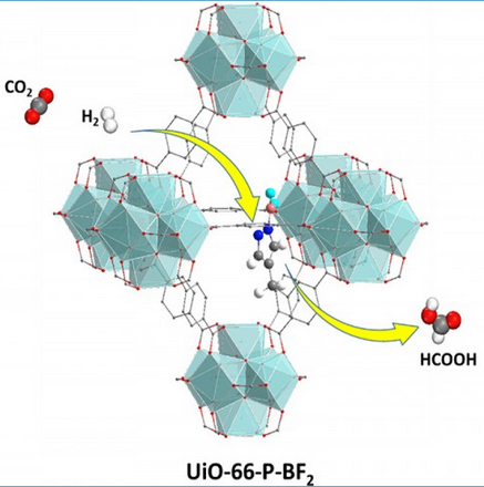
Using a novel catalyst, a single chemical assembly (UiO-66-P-BF2) could capture CO2 and also transform it and hydrogen into formic acid (HCOOH) via a two-step (yellow arrows) reaction (credit: Ye and Johnson/ACS Catalysis)

University of Pittsburgh researchers have invented (in computations) a cheap, efficient catalyst that would capture carbon dioxide (CO2) from coal-burning power plants before it reaches the atmosphere and converts the CO2  into formic acid — a valuable chemical that would create a revenue return. 

One current method for capturing CO2 uses Metal–organic frameworks (MOFs), which have a porous, cage-like structure that can absorb CO2, but require expensive catalysts, like platinum.

Instead, the researchers looked for lower-cost non-metallic catalysts, and found that a compound known as UiO-66-PBF2 would do the job.

The method is similar to one developed by Rice University using a combination of amine-rich compounds and carbon-60 molecules.

Those methods both differ from the “diamonds from the sky” approach, which turns CO2 from the air into carbon nanofibers, by capturing the CO2 before it leaves a smokestack. It will be interesting to compare these approaches in terms of CO2 capture efficiency, energy cost, and revenue return.

All three of these methods avoid the costs and energy expenditures from transporting and depositing CO2 at a storage site, required in carbon sequestration.


Abstract of Design of Lewis Pair-Functionalized Metal Organic Frameworks for CO2 Hydrogenation

Efficient catalytic reduction of CO2 is critical for the large-scale utilization of this greenhouse gas. We have used density functional electronic structure methods to design a catalyst for producing formic acid from CO2 and H2 via a two-step pathway having low reaction barriers. The catalyst consists of a microporous metal organic framework that is functionalized with Lewis pair moieties. These functional groups are capable of chemically binding CO2 and heterolytically dissociating H2. Our calculations indicate that the porous framework remains stable after functionalization and chemisorption of CO2 and H2. We have identified a low barrier pathway for simultaneous addition of hydridic and protic hydrogens to carbon and oxygen of CO2, respectively, producing a physisorbed HCOOH product in the pore. We find that activating H2 by dissociative adsorption leads to a much lower energy pathway for hydrogenating CO2 than reacting H2 with chemisorbed CO2. Our calculations provide design strategies for efficient catalysts for CO2 reduction.

3D-printed swimming microrobots can sense and remove toxins

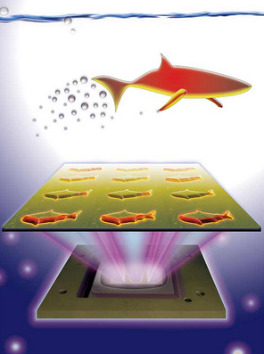
3D-printed microfish contain functional nanoparticles that enable them to be self-propelled, chemically powered and magnetically steered. The microfish are also capable of removing and sensing toxins. (credit: J. Warner, UC San Diego Jacobs School of Engineering)

A new kind of fish-shaped microrobots called “microfish” can swim around efficiently in liquids, are chemically powered by hydrogen peroxide, and magnetically controlled. They will inspire a new generation of “smart” microrobots that have diverse capabilities such as detoxification, sensing, and directed drug delivery, said nanoengineers at the University of California, San Diego.

To manufacture the microfish, the researchers used an innovative 3D printing technology they developed, with numerous improvements over other methods traditionally employed to create microrobots, such as microjet engines, microdrillers, and microrockets.

Most of these microrobots are incapable of performing more sophisticated tasks because they feature simple mechanical designs — such as spherical or cylindrical structures — and are made of homogeneous inorganic materials.

The research, led by Professors Shaochen Chen and Joseph Wang of the NanoEngineering Department at the UC San Diego, was published in the Aug. 12 issue of the journal Advanced Materials.

A microrobotic toxin scavenger

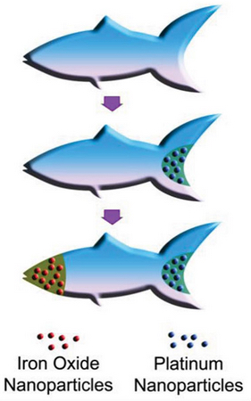
Platinum nanoparticles in the tail of the fish achieve propulsion via reaction with hydrogen peroxide; iron oxide nanoparticles are loaded into the head of the fish for magnetic control (credit: W. Zhu and J. Li, UC San Diego Jacobs School of Engineering)

The nanoengineers were able to easily add functional nanoparticles into certain parts of the microfish bodies.

They installed platinum nanoparticles in the tails, which react with hydrogen peroxide to propel the microfish forward, and magnetic iron oxide nanoparticles in the heads, which allowed them to be steered with magnets.

“We have developed an entirely new method to engineer nature-inspired microscopic swimmers that have complex geometric structures and are smaller than the width of a human hair.

With this method, we can easily integrate different functions inside these tiny robotic swimmers for a broad spectrum of applications,” said the co-first author Wei Zhu, a nanoengineering Ph.D. student in Chen’s research group at the Jacobs School of Engineering at UC San Diego.

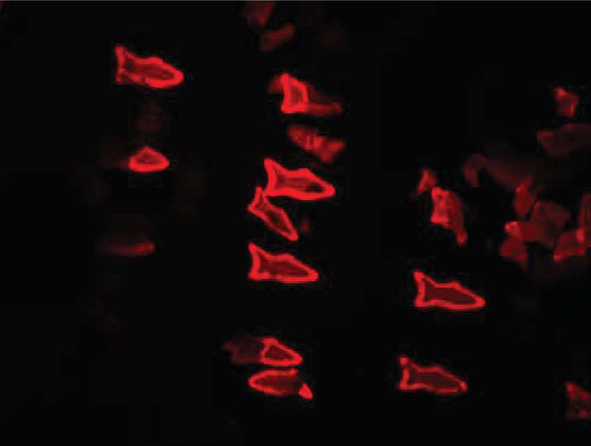
As a proof-of-concept demonstration, the researchers incorporated toxin-neutralizing polydiacetylene (PDA) nanoparticles throughout the bodies of the microfish to neutralize harmful pore-forming toxins such as the ones found in bee venom.

The researchers noted that the powerful swimming of the microfish in solution greatly enhanced their ability to clean up toxins.

When the PDA nanoparticles bind with toxin molecules, they become fluorescent and emit red-colored light. The team was able to monitor the detoxification ability of the microfish by the intensity of their red glow. “The neat thing about this experiment is that it shows how the microfish can doubly serve as detoxification systems and as toxin sensors,” said Zhu.

“Another exciting possibility we could explore is to encapsulate medicines inside the microfish and use them for directed drug delivery,” said Jinxing Li, the other co-first author of the study and a nanoengineering Ph.D. student in Wang’s research group.

3D-printing microrobots

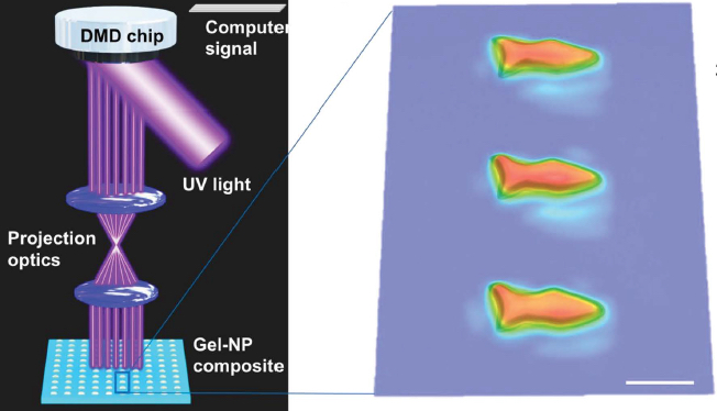
Schematic illustration of the μCOP method to fabricate microfish. (Left) UV light illuminates mirrors, generating an optical pattern specified by the control computer. The pattern is projected through optics onto the photosensitive monomer solution to fabricate the fish layer-by-layer. (Right) 3D microscopy image of an array of printed microfish. Scale bar, 100 micrometers. (credit: Wei Zhu et al./Advanced Materials)

The new microfish fabrication method is based on a rapid, high-resolution 3D printing technology called microscale continuous optical printing (μCOP) developed in Chen’s lab, offering speed, scalability, precision, and flexibility.

The key component of the μCOP technology is a digital micromirror array device (DMD) chip, which contains approximately two million micromirrors. Each micromirror is individually controlled to project UV light in the desired pattern (in this case, a fish shape) onto a photosensitive material, which solidifies upon exposure to UV light. The microfish are constructed one layer at a time, allowing each set of functional nanoparticles to be “printed” into specific parts of the fish bodies.

Fluorescent images demonstrating the detoxification capability of microfish containing encapsulated PDA nanoparticles (credit: Wei Zhu et al./Advanced Materials)

Within seconds, the researchers can print an array containing hundreds of microfish, each measuring 120 microns long and 30 microns thick. This process also does not require the use of harsh chemicals. Because the μCOP technology is digitized, the researchers could easily experiment with different designs for their microfish, including shark and manta ray shapes. They could also build microrobots in based on other biological organisms, such as birds, said Zhu.

“This method has made it easier for us to test different designs for these microrobots and to test different nanoparticles to insert new functional elements into these tiny structures. It’s my personal hope to further this research to eventually develop surgical microrobots that operate safer and with more precision,” said Li.


Abstract of 3D-Printed Artificial Microfish

Hydrogel microfish featuring biomimetic structures, locomotive capabilities, and functionalized nanoparticles are engineered using a rapid 3D printing platform: microscale continuous ­optical printing (μCOP). The 3D-printed ­microfish exhibit chemically powered and magnetically guided propulsion, as well as highly efficient detoxification capabilities that highlight the technical versatility of this platform for engineering advanced functional microswimmers for diverse biomedical applications.

MIT researchers invent process for 3D-printing complex transparent glass forms

Printing molten glass (credit: John Klein et al./3D Printing and Additive Manufacturing)

An additive-manufacturing glass-printing process called G3DP (Glass 3D Printing) has been developed by researchers in the Mediated Matter Group at the MIT Media Lab in collaboration with the Glass Lab at MIT.

Glass-printing platform. (1) Crucible, (2) heating elements, (3) nozzle (4) thermocouple, (5) removable feed access lid. (credit: John Klein et al./3D Printing and Additive Manufacturing)

The platform is based on a dual heated-chamber concept. The upper chamber acts as a Kiln Cartridge (a thermally insulated heater) operating at about 1900°F to melt the glass, while the lower chamber serves to anneal (form) the structures. The molten material gets funneled through an alumina-zircon-silica nozzle, which extrudes the material onto a build platform, where it cools and hardens. By tuning the form, transparency, and color variation, the process can drive, limit, or control light transmission, reflection and refraction in the final material.

Detail of a colored printed object (credit: John Klein et al./3D Printing and Additive Manufacturing)

The G3DP project was created in collaboration between the Mediated Matter group at the MIT Media Lab, the Mechanical Engineering Department, the MIT Glass Lab, and the Wyss Institute.

A selection of Glass pieces will appear in an exhibition at Cooper Hewitt, Smithsonian Design Museum, New York City in 2016.  An “Additive Manufacturing of Optically Transparent Glass” patent application was filed on April 25, 2014.


Mediated Matter Group | GLASS

‘Diamonds from the sky’ approach to turn CO2 into valuable carbon nanofibers

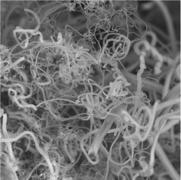
Researchers are removing a greenhouse gas from the air while generating carbon nanofibers like these (credit: Stuart Licht, Ph.D)

A research team of chemists at George Washington University has developed a technology that can economically convert atmospheric CO2 directly from the air into highly valued carbon nanofibers for industrial and consumer products — converting an anthropogenic greenhouse gas from a climate change problem to a valuable commodity, they say.

The team presented their research today (Aug. 19) at the 250th National Meeting & Exposition of the American Chemical Society (ACS).

“Such nanofibers are used to make strong carbon composites, such as those used in the Boeing Dreamliner, as well as in high-end sports equipment, wind turbine blades and a host of other products,” said Stuart Licht, Ph.D., team leader.

Previously, the researchers had made fertilizer and cement without emitting CO2, which they reported. Now, the team, which includes postdoctoral fellow Jiawen Ren, Ph.D., and graduate student Jessica Stuart, says their research could shift CO2 from a global-warming problem to a feed stock for the manufacture of in-demand carbon nanofibers.

Licht calls his approach “diamonds from the sky.” That refers to carbon being the material that diamonds are made of, and also hints at the high value of the products, such as carbon nanofibers.

A low-energy, high-efficiency process

The researchers claim this low-energy process can be run efficiently, using only a few volts of electricity, sunlight, and a whole lot of carbon dioxide. The system uses electrolytic syntheses to make the nanofibers. Here’s how:

  1. To power the syntheses, heat and electricity are produced through a hybrid and extremely efficient concentrating solar-energy system. The system focuses the sun’s rays on a photovoltaic solar cell to generate electricity and on a second system to generate heat and thermal energy, which raises the temperature of an electrolytic cell.
  2. CO2 is broken down in a high-temperature electrolytic bath of molten carbonates at 1,380 degrees F (750 degrees C).
  3. Atmospheric air is added to an electrolytic cell.
  4. The CO2 dissolves when subjected to the heat and direct current through electrodes of nickel and steel.
  5. The carbon nanofibers build up on the steel electrode, where they can be removed.

Licht estimates electrical energy costs of this “solar thermal electrochemical process” to be around $1,000 per ton of carbon nanofiber product. That means the cost of running the system is hundreds of times less than the value of product output, he says.

Decreasing CO2 to pre-industrial-revolution levels

“We calculate that with a physical area less than 10 percent the size of the Sahara Desert, our process could remove enough CO2 to decrease atmospheric levels to those of the pre-industrial revolution within 10 years,” he says.

At this time, the system is experimental. Licht’s biggest challenge will be to ramp up the process and gain experience to make consistently sized nanofibers. “We are scaling up quickly,” he adds, “and soon should be in range of making tens of grams of nanofibers an hour.”

Licht explains that one advance the group has recently achieved is the ability to synthesize carbon fibers using even less energy than when the process was initially developed. “Carbon nanofiber growth can occur at less than 1 volt at 750 degrees C, which for example is much less than the 3–5 volts used in the 1,000 degree C industrial formation of aluminum,” he says.

No published details on overall energy costs and efficiency are yet available (to be updated).


Abstract of New approach to carbon dioxide utilization: The carbon molten air battery

As the levels of carbon dioxide (CO2) increase in the Earth’s atmosphere, the effects on climate change become increasingly apparent. As the demand to reduce our dependence on fossils fuels and lower our carbon emissions increases, a transition to renewable energy sources is necessary. Cost effective large-scale electrical energy storage must be established for renewable energy to become a sustainable option for the future. We’ve previously shown that carbon dioxide can be captured directly from the air at solar efficiencies as high as 50%, and that carbon dioxide associated with cement formation and the production of other commodities can be electrochemically avoided in the STEP process.1-3

The carbon molten air battery, presented by our group in late 2013, is attractive due to its scalability, location flexibility, and construction from readily available resources, providing a battery that can be useful for large scale applications, such as the storage of renewable electricity.4

Uncommonly, the carbon molten air battery can utilize carbon dioxide directly from the air:
(1) charging: CO2(g) -> C(solid) + O2(g)
(2) discharging: C(solid) + O2(g) -> CO2(g)
More specifically, in a molten carbonate electrolyte containing added oxide, such as lithium carbonate with lithium oxide, the 4 electron charging reaction eq. 1 approaches 100% faradic efficiency and can be described as the following two equations:
(1a) O2-(dissolved) + CO2(g) -> CO32-(molten)
(1b) CO32-(molten) -> C(solid) + O2(g) + O2-(dissolved)
Thus, powered by carbon formed directly from the CO2 in our earth’s atmosphere, the carbon molten air battery is a viable system to provide large-scale energy storage.

1S. Licht, ”Efficient Solar-Driven Synthesis, Carbon Capture, and Desalinization, STEP: Solar Thermal Electrochemical Production of Fuels, Metals, Bleach,” Advanced Materials47, 5592 (2011).
2S. Licht, H. Wu, C. Hettige, B. Wang, J. Lau, J. Asercion, J. Stuart “STEP Cement: Solar Thermal Electrochemical Production of CaO without CO2 emission,” Chemical Communications, 48, 6019 (2012).
3S. Licht, B. Cui, B. Wang, F.-F. Li, J. Lau, S. Liu,” Ammonia synthesis by N2 and steam electrolysis in molten hydroxide suspensions of nanoscale Fe2O3,” Science, 345, 637 (2014).
4S. Licht, B. Cui, J. Stuart, B. Wang, J. Lau, “Molten Air Batteries – A new, highest energy class of rechargeable batteries,” Energy & Environmental Science, 6, 3646 (2013).

‘Armchair nanoribbon’ design makes graphene a wafer-scalable semiconductor

Progressively zoomed-in images of graphene nanoribbons grown on germanium (gray area). The ribbons automatically align perpendicularly and naturally grow in “armchair” edge configuration. (credit: Arnold Research Group and Guisinger Research Group)

University of Wisconsin-Madison engineers have discovered a way to grow graphene nanoribbons with semiconducting properties — and directly on a conventional germanium semiconductor wafer.

Graphene, an atom-thick material with extraordinary properties, normally functions as a conductor of electricity, but not as a semiconductor. This advance is significant because it could allow manufacturers to easily use graphene nanoribbons in hybrid integrated circuits, which promise to significantly boost the performance of next-generation electronic devices.

The technology could also have specific uses in high-performance industrial and military applications, such as sensors that detect specific chemical and biological species and photonic devices that manipulate light. More importantly, the technique promises to be easily scaled up for mass production and is compatible with the prevailing fab infrastructure used in semiconductor processing.

The development was announced in an open-access paper published Aug. 10 in the journal Nature Communications by Michael Arnold, an associate professor of materials science and engineering at UW-Madison, Ph.D. student Robert Jacobberger, and their collaborators.

How to create ultra-thin “armchair” graphene nanoribbons

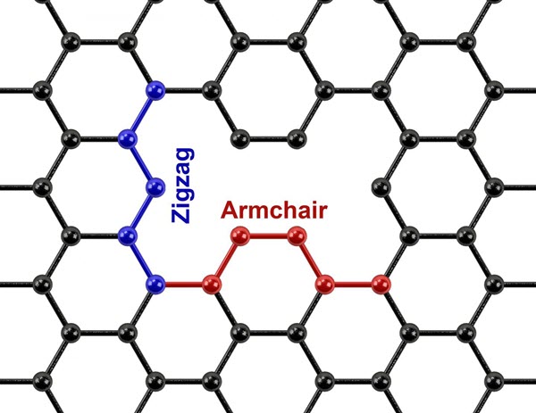
Armchair shape in graphene sheet (credit: Rajaram Narayanan/Jacobs School of Engineering/UC San Diego)

“Graphene nanoribbons that can be grown directly on the surface of a semiconductor like germanium are more compatible with planar processing that’s used in the semiconductor industry, and so there would be less of a barrier to integrating these really excellent materials into electronics in the future,” Arnold says.

Graphene, a sheet of carbon atoms that is only one atom in thickness, conducts electricity and dissipates heat much more efficiently than silicon, the material most commonly found in today’s computer chips.

But to exploit graphene’s remarkable electronic properties in semiconductor applications where current must be switched on and off, graphene nanoribbons need to be less than 10 nanometers wide. In addition, the nanoribbons must have smooth, well-defined “armchair” edges in which the carbon-carbon bonds are parallel to the length of the ribbon.

Researchers have typically fabricated nanoribbons by using lithographic techniques to cut larger sheets of graphene into ribbons. However, this “top-down” fabrication approach lacks precision and produces nanoribbons with very rough edges.

Another strategy for making nanoribbons is to use a “bottom-up” approach such as surface-assisted organic synthesis, where molecular precursors react on a surface to polymerize nanoribbons. Arnold says surface-assisted synthesis can produce beautiful nanoribbons with precise, smooth edges, but this method only works on metal substrates and the resulting nanoribbons are thus far too short for use in electronics.

Chemical vapor deposition process breakthrough

To overcome these hurdles, the UW-Madison researchers pioneered a bottom-up technique in which they grow ultra-narrow nanoribbons with smooth, straight edges directly on germanium wafers using a process called chemical vapor deposition. In this process, the researchers start with methane, which adsorbs to the germanium surface and decomposes to form various hydrocarbons. These hydrocarbons react with each other on the surface, where they form graphene.

Arnold’s team made its discovery when it explored dramatically slowing the growth rate of the graphene crystals by decreasing the amount of methane in the chemical vapor deposition chamber. They found that at a very slow growth rate, the graphene crystals naturally grow into long nanoribbons on a specific crystal facet of germanium. By simply controlling the growth rate and growth time, the researchers can easily tune the nanoribbon width be to less than 10 nanometers.

“What we’ve discovered is that when graphene grows on germanium, it naturally forms nanoribbons with these very smooth, armchair edges,” Arnold says. “The widths can be very, very narrow and the lengths of the ribbons can be very long, so all the desirable features we want in graphene nanoribbons are happening automatically with this technique.”

The nanoribbons produced with this technique start nucleating, or growing, at seemingly random spots on the germanium and are oriented in two different directions on the surface. Arnold says the team’s future work will include controlling where the ribbons start growing and aligning them all in the same direction.

The researchers are patenting their technology through the Wisconsin Alumni Research Foundation. The research was primarily supported by the Department of Energy’s Basic Energy Sciences program.


Abstract of Direct oriented growth of armchair graphene nanoribbons on germanium

Graphene can be transformed from a semimetal into a semiconductor if it is confined into nanoribbons narrower than 10 nm with controlled crystallographic orientation and well-defined armchair edges. However, the scalable synthesis of nanoribbons with this precision directly on insulating or semiconducting substrates has not been possible. Here we demonstrate the synthesis of graphene nanoribbons on Ge(001) via chemical vapour deposition. The nanoribbons are self-aligning 3° from the Geleft fence110right fence directions, are self-defining with predominantly smooth armchair edges, and have tunable width to <10 nm and aspect ratio to >70. In order to realize highly anisotropic ribbons, it is critical to operate in a regime in which the growth rate in the width direction is especially slow, <5 nm h−1. This directional and anisotropic growth enables nanoribbon fabrication directly on conventional semiconductor wafer platforms and, therefore, promises to allow the integration of nanoribbons into future hybrid integrated circuits.