Glass paint could keep metal roofs and other structures cool even on sunny days

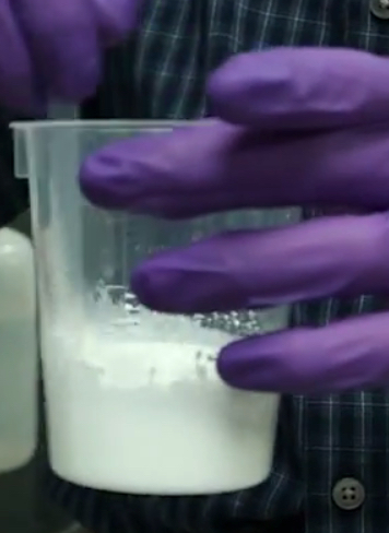
Silica-based paint (credit: American Chemical Society/Johns Hopkins University Applied Physics Lab)

Scientists at the Johns Hopkins University Applied Physics Lab have developed a new, environmentally friendly paint made from glass that bounces sunlight off metal surfaces — keeping them cool and durable.

“Most paints you use on your car or house are based on polymers, which degrade in the ultraviolet light rays of the sun,” says Jason J. Benkoski, Ph.D. “So over time you’ll have chalking and yellowing. Polymers also tend to give off volatile organic compounds, which can harm the environment. That’s why I wanted to move away from traditional polymer coatings to inorganic glass ones.”

Glass, which is made out of silica, would be an ideal coating. It’s hard, durable and has the right optical properties. But it’s very brittle.

To address that aspect in a new coating, Benkoski, started with silica, one of the most abundant materials in the earth’s crust. He modified one version of it, potassium silicate, that normally dissolves in water. His tweaks transformed the compound so that when it’s sprayed onto a surface and dries, it becomes water-resistant.

Unlike acrylic, polyurethane or epoxy paints, Benkoski’s paint is almost completely inorganic, which should make it last far longer than its counterparts that contain organic compounds. His paint is also designed to expand and contract with metal surfaces to prevent cracking.

Mixing pigments with the silicate gives the coating an additional property: the ability to reflect all sunlight and passively radiate heat. Since it doesn’t absorb sunlight, any surface coated with the paint will remain at air temperature, or even slightly cooler. That’s key to protecting structures from the sun.

“When you raise the temperature of any material, any device, it almost always by definition ages much more quickly than it normally would,” Benkoski says. “It’s not uncommon for aluminum in direct sunlight to heat 70 degrees Fahrenheit above ambient temperature. If you make a paint that can keep an outdoor surface close to air temperature, then you can slow down corrosion and other types of degradation.”


American Chemical Society | Glass Paint That Can Keep Structures Cool

The paint Benkoski’s lab is developing is intended for use on naval ships (with funding from the U.S. Office of Naval Research), but has many potential commercial applications.

“You might want to paint something like this on your roof to keep heat out and lower your air-conditioning bill in the summer,” he says. It could even go on metal playground slides or bleachers. And it would be affordable. The materials needed to make the coating are abundant and inexpensive.”

Benkoski says he expects his lab will start field-testing the material in about two years.

The researchers presented their work today at the 250th National Meeting & Exposition of the American Chemical Society (ACS), held in Boston through Thursday. It features more than 9,000 presentations on a wide range of science topics.


Abstract of Passive cooling with UV-resistant siloxane coatings in direct sunlight

Solar exposure is a leading cause of material degradation in outdoor use. Polymers and other organic materials photo-oxidize due to ultraviolet (UV) exposure. Even in metals, solar heating can cause unwanted property changes through precipitation and Ostwald ripening. In more complex systems, cyclic temperature changes cause fatigue failure wherever thermal expansion mismatch occurs. Most protective coatings designed to prevent these effects inevitably succumb to the same phenomena because of their polymeric matrix. In contrast, siloxane coatings have the potential provide indefinite solar protection because they do not undergo photo-oxidation. This study therefore demonstrates UV-reflective siloxane coatings with low solar absorptance and high thermal emissivity that prevent any increase in temperature above ambient conditions in direct sunlight. Mathematical modeling suggests that even sub-ambient cooling is possible for ZnO-filled potassium silicate. Preventing widespread adoption of potassium silicates until now has been their tendency to crack at large thicknesses, dissolve in water, and delaminate from untreated surfaces. This investigation has successfully addressed these limitations by formulating potassium silicates to behave more like a flexible siloxane polymer than a brittle inorganic glass. The addition of plasticizers (potassium, glycerol), gelling agents (polyethylenimine), and water-insoluble precipitates (zinc silicates, cerium silicates, organosilanes) make it possible to form thick, water resistant coatings that exhibit excellent adhesion even to untreated aluminum surfaces.

New solid-state memory technology allows for highest-density non-volatile storage

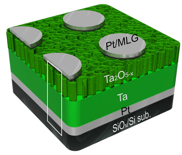
A schematic shows the layered structure of new type of solid-state memory developed at Rice University (credit: Tour Group/Rice University)

Scientists in the Rice University lab of chemist James Tour have created a solid-state memory technology that allows for high-density 162 gigabits nonvolatile storage, much higher than other oxide-based memory systems under investigation by scientists. (Eight bits equal one byte; a 162-gigabit unit would store about 20 gigabytes of information.)

Applying voltage to a 250-nanometer-thick sandwich of graphene, tantalum, nanoporous tantalum oxide (an insulator), and platinum creates addressable bits where the layers meet. Control voltages shift oxygen ions and vacancies to switch the bits between ones and zeroes.

Like the Tour lab’s previous discovery of silicon oxide memories, the new devices require only two electrodes per circuit, making them simpler than present-day flash memories, which use three. “This is a new way to make ultradense, nonvolatile computer memory,” Tour said.

Nonvolatile random-access memories, such as such as flash memory in smartphones and tablets, hold their data even when the power is off, unlike volatile random-access computer memories (in most computers), which lose their contents when the machine is shut down.

Modern memory chips have many requirements: They have to read and write data at high speed and hold as much as possible. They must also be durable and show good retention of that data while using minimal power. These are provided by Rice’s new design, which requires only one hundredth the amount of energy required with present devices, Tour says.

“This tantalum memory is based on two-terminal systems, so it’s all set for 3-D memory stacks,” he said. “And it doesn’t even need diodes or selectors, making it one of the easiest ultradense memories to construct. This will be a real competitor for the growing memory demands in high-definition video storage and server arrays.”

A layered structure of tantalum, tantalum oxide, multilayer graphene, and platinum is the basis for a new type of nonvolatile memory (credit: Tour Group/Rice University)

In making the material, the researchers found the tantalum oxide gradually loses oxygen ions, changing from an oxygen-rich, nanoporous semiconductor at the top to oxygen-poor at the bottom. Where the oxygen disappears completely, it becomes pure tantalum, a metal. The graphene does double duty as a barrier that keeps platinum from migrating into the tantalum oxide and causing a short circuit.*


Rice University | Tantalum oxide memory: Slices taken from a tantalum oxide-based memory developed at Rice University show the partially interconnected and randomly distributed internal pores in the material.

Tour said tantalum oxide memories can be fabricated at room temperature. He noted the control voltage that writes and rewrites the bits is adjustable, which allows a wide range of switching characteristics.

(As the researchers note in a paper in the journal Nano Letters, nonvolatile resistive oxide-based memories can also offer faster switching speed. That suggests that tantalum oxide memories might one day further improve MIT’s “BlueDBM” solution for improved handling of big data by making nonvolatile memory more efficient, as described on KurzweilAI last week.)

The remaining hurdles to commercialization of tantalum oxide memories include the fabrication of a dense enough crossbar device to address individual bits and a way to control the size of the nanopores.

The research is described online in the American Chemical Society Researchers at Korea University-Korea Institute of Science and Technology and University of Massachusetts, Amherst where also involved.

Tour is the T.T. and W.F. Chao Chair in Chemistry as well as a professor of materials science and nanoengineering and of computer science and a member of Rice’s Richard E. Smalley Institute for Nanoscale Science and Technology.


Rice University | Tantalum oxide memory 2

* The researchers determined three related factors give the memories their unique switching ability:

  • The control voltage mediates how electrons pass through a boundary that can flip from an ohmic (current flows in both directions) to a Schottky (current flows one way) contact and back.
  • The boundary’s location can change based on oxygen vacancies. These are “holes” in atomic arrays where oxygen ions should exist, but don’t. The voltage-controlled movement of oxygen vacancies shifts the boundary from the tantalum/tantalum oxide interface to the tantalum oxide/graphene interface. “The exchange of contact barriers causes the bipolar switching,” said Gunuk Wang, lead author of the study and a former postdoctoral researcher at Rice.
  • The flow of current draws oxygen ions from the tantalum oxide nanopores and stabilizes them. These negatively charged ions produce an electric field that effectively serves as a diode to hinder error-causing crosstalk. While researchers already knew the potential value of tantalum oxide for memories, such arrays have been limited to about a kilobyte because denser memories suffer from crosstalk that allows bits to be misread.

Abstract of Three-Dimensional Networked Nanoporous Ta2O5–x Memory System for Ultrahigh Density Storage

Oxide-based resistive memory systems have high near-term promise for use in nonvolatile memory. Here we introduce a memory system employing a three-dimensional (3D) networked nanoporous (NP) Ta2O5–x structure and graphene for ultrahigh density storage. The devices exhibit a self-embedded highly nonlinear I–V switching behavior with an extremely low leakage current (on the order of pA) and good endurance. Calculations indicated that this memory architecture could be scaled up to a ∼162 Gbit crossbar array without the need for selectors or diodes normally used in crossbar arrays. In addition, we demonstrate that the voltage point for a minimum current is systematically controlled by the applied set voltage, thereby offering a broad range of switching characteristics. The potential switching mechanism is suggested based upon the transformation from Schottky to Ohmic-like contacts, and vice versa, depending on the movement of oxygen vacancies at the interfaces induced by the voltage polarity, and the formation of oxygen ions in the pores by the electric field.

Electro-optical modulator is 100 times smaller, consumes 100th of the energy

Colorized electron microscope image of a micro-modulator made of gold. In the slit in the center of the picture, light is converted into plasmon polaritons, modulated, and then re-converted into light pulses (credit: Haffner et al. Nature Photonics)

Researchers at ETH Zurich have developed a modulator that is a 100 times smaller than conventional modulators, so it can now be integrated into electronic circuits. Transmitting large amounts of data via the Internet requires high-performance electro-optic modulators — devices that convert electrical signals (used in computers and cell phones) into light signals (used in fiber-optic cables).

Today, huge amounts of data are sent incredibly fast through fiber-optic cables as light pulses. For that purpose they first have to be converted from electrical signals, which are used by computers and telephones, into optical signals. Today’s electro-optic modulators are more complicated and large, compared with electronic devices that can be as small as a few micrometers.

The plasmon trick

To build the smallest possible modulator they first need to focus a light beam whose intensity they want to modulate into a very small volume. The laws of optics, however, dictate that such a volume cannot be smaller than the wavelength of the light itself. Modern telecommunications use near-infrared laser light with a wavelength of 1500 nanometers (1.5 micrometers), which sets the lower limit for the size of a modulator.

To beat that limit and to make the device even smaller, the light is first turned into surface-plasmon-polaritons. Plasmon-polaritons are a combination of electromagnetic fields and electrons that propagate along a surface of a metal strip. At the end of the strip they are converted back to light once again. The advantage of this detour is that plasmon-polaritons can be confined in a much smaller space than the light they originated from.

The modulator is much smaller than conventional devices so it consumes very little energy — only a few thousandth of a Watt at a data transmission rate of 70 Gigabits per second. This corresponds to about 100th of the energy consumption of commercial models. And that means more data can be transmitted at higher speeds. The device is also cheaper to produce.

The research is described in a paper in the journal Nature Photonics.


Abstract of All-plasmonic Mach–Zehnder modulator enabling optical high-speed communication at the microscale

Optical modulators encode electrical signals to the optical domain and thus constitute a key element in high-capacity communication links. Ideally, they should feature operation at the highest speed with the least power consumption on the smallest footprint, and at low cost. Unfortunately, current technologies fall short of these criteria. Recently, plasmonics has emerged as a solution offering compact and fast devices. Yet, practical implementations have turned out to be rather elusive. Here, we introduce a 70 GHz all-plasmonic Mach–Zehnder modulator that fits into a silicon waveguide of 10 μm length. This dramatic reduction in size by more than two orders of magnitude compared with photonic Mach–Zehnder modulators results in a low energy consumption of 25 fJ per bit up to the highest speeds. The technology suggests a cheap co-integration with electronics.

‘Plasmonic’ material could bring ultrafast all-optical communications

This rendering depicts a new “plasmonic oxide material” that could make possible devices for optical communications that are at least 10 times faster than conventional technologies (credit: Purdue University/Nathaniel Kinsey)

Researchers at Purdue University have created a new “plasmonic oxide material” that could make possible modulator devices for optical communications (fiber optics, used for the Internet and cable television) that are at least 10 times faster than conventional technologies.

The optical material, made of aluminum-doped zinc oxide (AZO) also requires less power than other “all-optical” semiconductor devices. That is essential for the faster operation, which would otherwise generate excessive heat with the increase transmission speed.

The material has been shown to work in the near-infrared range of the spectrum, which is used in optical communications, and it is compatible with the CMOS semiconductor manufacturing process used to construct integrated circuits.

Faster optical transistors replace silicon

The researchers have proposed creating an “all-optical plasmonic modulator using CMOS-compatible materials,” or an optical transistor, which allows for the speedup compared to systems that use silicon chips.

A cycle takes about 350 femtoseconds to complete in the new AZO films, which is roughly 5,000 times faster than crystalline silicon.

The researchers “doped” zinc oxide with aluminum (thus the AZO), meaning the zinc oxide is impregnated with aluminum atoms to alter the material’s optical properties. Doping the zinc oxide causes it to behave like a metal at certain wavelengths and like a dielectric at other wavelengths.

The AZO also makes it possible to “tune” the optical properties of metamaterials.

Findings were detailed in an open-access research paper appearing in July in the journal Optica, published by the Optical Society of America.

The ongoing research is funded by the Air Force Office of Scientific Research, a Marie Curie Outgoing International Fellowship, the National Science Foundation, and the Office of Naval Research.


Abstract of Epsilon-near-zero Al-doped ZnO for ultrafast switching at telecom wavelengths

Transparent conducting oxides have recently gained great attention as CMOS-compatible materials for applications in nanophotonics due to their low optical loss, metal-like behavior, versatile/tailorable optical properties, and established fabrication procedures. In particular, aluminum-doped zinc oxide (AZO) is very attractive because its dielectric per-mittivity can be engineered over a broad range in the near-IR and IR. However, despite all these beneficial features, the slow (>100 ps) electron-hole recombination time typical of these compounds still represents a fundamental limitation impeding ultrafast optical modulation. Here we report the first epsilon-near-zero AZO thin films that simultaneously exhibit ultrafast carrier dynamics (excitation and recombination time below 1 ps) and an outstanding reflectance modulation up to 40% for very low pump fluence levels (<4 mJ∕cm2) at a telecom wavelength of 1.3 μm. The unique properties of the demonstrated AZO thin films are the result of a low-temperature fabrication procedure promoting deep-level defects within the film and an ultrahigh carrier concentration. © 2015 Optical Society of America

Unlikely graphene-nanotube combination forms high-speed digital switch

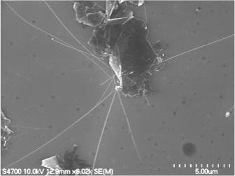
Hair-like boron nitride nanotubes intersect a sheet of graphene (top) to create a high-speed digital switch (credit: Michigan Tech, Yoke Khin Yap)

By themselves, graphene is too conductive while boron nitride nanotubes are too insulating, but combining them could create a workable digital switch — which can be used for controlling electrons in computers and other electronic devices.

To create this serendipitous super-hybrid, Yoke Khin Yap, a professor of physics at Michigan Technological University, and his team exfoliated (peeled off) graphene(from graphite) and modified the material’s surface with tiny pinholes, then grew the boron nitride nanotubes up and through the pinholes — like a plant randomly poking up through a crack in a concrete pavement. That formed a “band gap” mismatch, which created “a potential barrier  that stops electrons,” he said.

In other words, a switch.

The chemical structures of graphene (gray) and boron nitride nanotubes (pink and purple) can be used to create a digital switch at the point where the two materials come in contact (credit: Michigan Tech, Yoke Khin Yap)

High switching speed

The band gap mismatch results from the materials’ structure: graphene’s flat sheet conducts electricity quickly, and the atomic structure in the nanotubes halts electric currents. This disparity creates a barrier, caused by the difference in electron movement as currents move next to and past the hair-like boron nitride nanotubes. These points of contact between the materials, called heterojunctions, are what make the digital on/off switch possible.

Yap and his research team have also shown that because the materials are respectively so effective at conducting or stopping electricity, the resulting switching ratio is high. So how fast the materials can turn on and off is several orders of magnitude greater than current graphene switches. And this speed could eventually quicken the pace of electronics and computing.

Yap says this study is a continuation of past research into making transistors without semiconductors. The problem with semiconductors like silicon is that they can only get so small, and they give off a lot of heat; the use of graphene and nanotubes bypasses those problems. In addition, the graphene and boron nitride nanotubes have the same atomic arrangement pattern, or lattice matching. With their aligned atoms, the graphene-nanotube digital switches could avoid the issues of electron scattering.

“You want to control the direction of the electrons,” Yap explains, comparing the challenge to a pinball machine that traps, slows down and redirects electrons. “This is difficult in high speed environments, and the electron scattering reduces the number and speed of electrons.”

The journal Scientific Reports recently published their work in an open-access paper.


Abstract of Switching Behaviors of Graphene-Boron Nitride Nanotube Heterojunctions

High electron mobility of graphene has enabled their application in high-frequency analogue devices but their gapless nature has hindered their use in digital switches. In contrast, the structural analogous, h-BN sheets and BN nanotubes (BNNTs) are wide band gap insulators. Here we show that the growth of electrically insulating BNNTs on graphene can enable the use of graphene as effective digital switches. These graphene-BNNT heterojunctions were characterized at room temperature by four-probe scanning tunneling microscopy (4-probe STM) under real-time monitoring of scanning electron microscopy (SEM). A switching ratio as high as 105 at a turn-on voltage as low as 0.5 V were recorded. Simulation by density functional theory (DFT) suggests that mismatch of the density of states (DOS) is responsible for these novel switching behaviors.

How to tune graphene properties by introducing defects

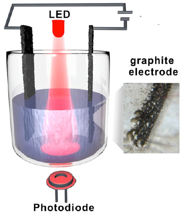
Exfoliation setup. Inset: graphite electrode during exfoliation (credit: Mario Hofmann/Nanotechnology)

Taiwanese researchers reported today (July 30) in the journal Nanotechnology that they have developed a simple electrochemical approach that allows for defects to intentionally be created in graphene, altering its electrical and mechanical properties and making the material more useful for electronic devices and drug delivery, for example.

Current graphene synthesis techniques, such as chemical vapor deposition and reduction of graphene oxide, can only produce graphene with a narrow range of characteristics, limiting the usefulness of produced graphene, the researchers say.

The researchers used a technique called electrochemical synthesis to exfoliate, or peel off graphite flakes into graphene layers. By varying the pulsed voltage, they could change the resulting graphene’s thickness, flake area, and number of defects, altering the properties of graphene.

They also found they need to use a solvent for intercalation (adding a fluid or material between layers) as the necessary first step.

To monitor the evolution of the graphene in the solvent they found that simply tracking the solution’s transparency with an LED and photodiode could give them quantitative information on the efficiency and onset of exfoliation.

They next plan to study the effects of adjusting the pulse durations throughout the exfoliation process to improve the amount of exfoliated graphene and to introduce more complex pulse shapes to selectively produce certain types of graphene defects.


Abstract of Controlling the properties of graphene produced by electrochemical exfoliation

The synthesis of graphene with controllable electronic and mechanical characteristics is of significant importance for its application in various fields ranging from drug delivery to energy storage. Electrochemical exfoliation of graphite has yielded graphene with widely varying behavior and could be a suitable approach. Currently, however the limited understanding of the exfoliation process obstructs targeted modification of graphene properties. We here investigate the process of electrochemical exfoliation and the impact of its parameters on the produced graphene. Using in situ optical and electrical measurements we determine that solvent intercalation is the required first step and the degree of intercalation controls the thickness of the exfoliated graphene. Electrochemical decomposition of water into gas bubbles causes the expansion of graphite and controls the functionalization and lateral size of the exfoliated graphene. Both process steps proceed at different time scales and can be individually addressed through application of pulsed voltages. The potential of the presented approach was demonstrated by improving the performance of graphene-based transparent conductors by 30 times.

How hybrid solar-cell materials may capture more solar energy

Innovative techniques for reducing solar-cell installation costs by capturing more solar energy per unit area by using hybrid materials have recently been announced by two universities.

Capturing more of the spectrum

Chemists at the University of California, Riverside have found an ingenious way to lower solar cell installation costs by reducing the size of solar collectors (credit: David Monniaux)

The University of California, Riverside strategy for making solar cells more efficient is to use the near-infrared region of the sun’s spectrum, which is not absorbed by current solar cells.

The researchers report in Nano Letters that a hybrid material that combines inorganic materials (cadmium selenide and lead selenide semiconductor nanocrystals) with organic molecules (diphenylanthracene and rubrene) could allow for an increase of solar photovoltaic efficiency by 30 percent or more, according to Christopher Bardeen, a UC Riverside professor of chemistry.

The new material also has wide-ranging applications such as in biological imaging, data storage and organic light-emitting diodes. “The ability to move light energy from one wavelength to [a] more useful region — for example, from red to blue — can impact any technology that involves photons as inputs or outputs,” he said.

The research was supported by grants from the National Science Foundation and the U.S. Army.

Plasmonic nanostructures and metal oxides

Rice researchers selectively filtered high-energy hot electrons from their less-energetic counterparts using a Schottky barrier (left) created with a gold nanowire on a titanium dioxide semiconductor. A second setup (right), which included a thin layer of titanium between the gold and the titanium dioxide, did not filter electrons based on energy level. (credit: B. Zheng/Rice University)

Meanwhile, new research from Rice’s Laboratory for Nanophotonics (LANP) has found a way to boost the efficiency and also reduce the cost of photovoltaic solar cells by using high-efficiency light-gathering plasmonic nanostructures combined with low-cost semiconductors, such as metal oxides.

“We can tune plasmonic structures to capture light across the entire solar spectrum,” claims Rice’s Naomi Halas, co-author of an open-access paper in Nature Communications. “The efficiency of [conventional] semiconductor-based solar cells can never be extended in this way because of the inherent optical properties of the semiconductors.”

The researchers found in an experiment that a solar cell using a “Schottky barrier” device allowed only “hot electrons” (electrons in the metal that have a much higher energy level) to pass from a gold nanowire to the semiconductor, unlike an “Ohmic device,” which let all electrons pass.

Today’s most efficient photovoltaic cells use a combination of semiconductors that are made from rare and expensive elements like gallium and indium, so this finding promises to further reduce the cost of solar cells.


Abstract of Hybrid Molecule–Nanocrystal Photon Upconversion Across the Visible and Near-Infrared

The ability to upconvert two low energy photons into one high energy photon has potential applications in solar energy, biological imaging, and data storage. In this Letter, CdSe and PbSe semiconductor nanocrystals are combined with molecular emitters (diphenylanthracene and rubrene) to upconvert photons in both the visible and the near-infrared spectral regions. Absorption of low energy photons by the nanocrystals is followed by energy transfer to the molecular triplet states, which then undergo triplet–triplet annihilation to create high energy singlet states that emit upconverted light. By using conjugated organic ligands on the CdSe nanocrystals to form an energy cascade, the upconversion process could be enhanced by up to 3 orders of magnitude. The use of different combinations of nanocrystals and emitters shows that this platform has great flexibility in the choice of both excitation and emission wavelengths.

Abstract of Distinguishing between plasmon-induced and photoexcited carriers in a device geometry

The use of surface plasmons, charge density oscillations of conduction electrons of metallic nanostructures, to boost the efficiency of light-harvesting devices through increased light-matter interactions could drastically alter how sunlight is converted into electricity or fuels. These excitations can decay directly into energetic electron–hole pairs, useful for photocurrent generation or photocatalysis. However, the mechanisms behind plasmonic carrier generation remain poorly understood. Here we use nanowire-based hot-carrier devices on a wide-bandgap semiconductor to show that plasmonic carrier generation is proportional to internal field-intensity enhancement and occurs independently of bulk absorption. We also show that plasmon-induced hot electrons have higher energies than carriers generated by direct excitation and that reducing the barrier height allows for the collection of carriers from plasmons and direct photoexcitation. Our results provide a route to increasing the efficiency of plasmonic hot-carrier devices, which could lead to more efficient devices for converting sunlight into usable energy.

Super-elastic conducting fibers for artificial muscles, sensors, capacitors

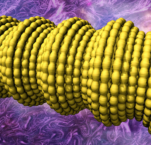
UT Dallas scientists have constructed novel fibers by wrapping sheets of tiny carbon nanotubes to form a sheath around a long rubber core. This illustration shows complex two-dimensional buckling, shown in yellow, of the carbon nanotube sheath/rubber-core fiber. The buckling results in a conductive fiber with super elasticity and novel electronic properties. (credit: UT Dallas Alan G. MacDiarmid Nanotech Institute)

An international research team based at The University of Texas at Dallas has made electrically conducting fibers that can be reversibly stretched to more than 14 times their initial length and whose electrical conductivity increases 200-fold when stretched.

The research team is using the new fibers to make artificial muscles, as well as capacitors with energy storage capacity that increases about tenfold when the fibers are stretched.

Fibers and cables derived from the invention might one day be used as interconnects for super-elastic electronic circuits, robots and exoskeletons having great reach, morphing aircraft, giant-range strain sensors, failure-free pacemaker leads, and super-stretchy charger cords for electronic devices.

Wrapping carbon nanotube sheets into fibers

In a study published in the July 24 issue of the journal Science, the scientists describe how they constructed the fibers by wrapping lighter-than-air, electrically conductive sheets of tiny carbon nanotubes to form a jelly-roll-like sheath around a long rubber core.

The new fibers differ from conventional materials in several ways. For example, when conventional fibers are stretched, the resulting increase in length and decrease in cross-sectional area restricts the flow of electrons through the material. But even a “giant” stretch of the new conducting sheath-core fibers causes little change in their electrical resistance, said Dr. Ray Baughman, senior author of the paper and director of the Alan G. MacDiarmid NanoTech Institute at UT Dallas.

One key to the performance of the new conducting elastic fibers is the introduction of buckling into the carbon nanotube sheets. Because the rubber core is stretched along its length as the sheets are being wrapped around it, when the wrapped rubber relaxes, the carbon nanofibers form a complex buckled structure, which allows for repeated stretching of the fiber.

“Think of the buckling that occurs when an accordion is compressed, which makes the inelastic material of the accordion stretchable,” said Baughman, the Robert A. Welch Distinguished Chair in Chemistry at UT Dallas.

“We make the inelastic carbon nanotube sheaths of our sheath-core fibers super stretchable by modulating large buckles with small buckles, so that the elongation of both buckle types can contribute to elasticity. These amazing fibers maintain the same electrical resistance, even when stretched by giant amounts, because electrons can travel over such a hierarchically buckled sheath as easily as they can traverse a straight sheath.”

Radical electronic and mechanical devices possible

By adding a thin overcoat of rubber to the sheath-core fibers and then another carbon nanotube sheath, the researchers made strain sensors and artificial muscles in which the buckled nanotube sheaths serve as electrodes and the thin rubber layer is a dielectric, resulting in a fiber capacitor. These fiber capacitors exhibited the unrivaled capacitance change of 860 percent when the fiber was stretched 950 percent.

Adding twist to these double-sheath fibers resulted in fast, electrically powered torsional — or rotating — artificial muscles that could be used to rotate mirrors in optical circuits or pump liquids in miniature devices used for chemical analysis. The conducting elastomers can be fabricated in diameters ranging from the very small — about 150 microns, or twice the width of a human hair — to much larger sizes, depending on the size of the rubber core. Individual small fibers also can be combined into large bundles and plied together like yarn or rope,” according to the researchers.

“This technology could be well-suited for rapid commercialization,” said Dr. Raquel Ovalle-Robles MS’06 PhD’08, an author on the paper and chief research and intellectual properties strategist at Lintec of America’s Nano-Science & Technology Center.

“The rubber cores used for these sheath-core fibers are inexpensive and readily available,” she said. “The only exotic component is the carbon nanotube aerogel sheet used for the fiber sheath.”


UT Dallas | UT Dallas Nanotech CNT rubber fiber

In this video, two lab demonstrations show the near invariance of resistance during the stretching of carbon-nanotube-sheathed rubber fibers.


UT Dallas Comets |UTD Nanotech pacemaker lead demo


Abstract of Hierarchically buckled sheath-core fibers for superelastic electronics, sensors, and muscles

Superelastic conducting fibers with improved properties and functionalities are needed for diverse applications. Here we report the fabrication of highly stretchable (up to 1320%) sheath-core conducting fibers created by wrapping carbon nanotube sheets oriented in the fiber direction on stretched rubber fiber cores. The resulting structure exhibited distinct short- and long-period sheath buckling that occurred reversibly out of phase in the axial and belt directions, enabling a resistance change of less than 5% for a 1000% stretch. By including other rubber and carbon nanotube sheath layers, we demonstrated strain sensors generating an 860% capacitance change and electrically powered torsional muscles operating reversibly by a coupled tension-to-torsion actuation mechanism. Using theory, we quantitatively explain the complementary effects of an increase in muscle length and a large positive Poisson’s ratio on torsional actuation and electronic properties.

Novel DNA origami structures

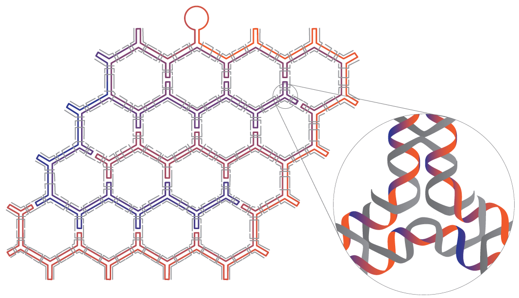
The versatility of the DNA origami 3D wireframe design technique created by Arizona State University Biodesign Institute researcher Hao Yan is demonstrated with the construction of this snub cube model, an Archimedean solid with 60 edges, 24 vertices and 38 faces including 6 squares and 32 equilateral triangles. (credit: TED-43/Wikimedia Commons)

Hao Yan, a researcher at Arizona State University’s Biodesign Institute, has extended DNA origami — which uses combinations of DNA base pairs to create new 2-D and 3-D nanoforms — into imaginative new forms that may one day lead to microelectronics and biomedical innovations.

“Earlier design methods [for DNA origami] used strategies including parallel arrangement of DNA helices to approximate arbitrary shapes, but precise fine-tuning of DNA wireframe architectures that connect vertices in 3D space has required a new approach,” says Yan, the Milton D. Glick Distinguished Chair of Chemistry and Biochemistry at ASU and directs Biodesign’s Center for Molecular Design and Biomimetics.

The new study describes wireframe structures of high complexity and programmability that are fabricated by precise control of branching and curvature, using novel organizational principles for the designs. (Wireframes are skeletal three-dimensional models represented purely through lines and vertices.)

The resulting nanoforms include symmetrical lattice arrays, quasicrystalline structures, curvilinear arrays, and a simple wire art sketch in the 100-nm scale, as well as 3-D objects including a snub cube with 60 edges and 24 vertices and a reconfigurable Archimedean solid that can be controlled to make the unfolding and refolding transitions between 3D and 2D.

The research appears in the advanced online edition of the journal Nature Nanotechnology.


DNA origami: how it works

In previous investigations, the Yan group created subtle architectural forms at an astonishingly minute scale, some measuring only tens of nanometers across — roughly the diameter of a virus particle. These nano-objects include spheres, spirals, flasksMöbius forms, and even an autonomous spider-like robot capable of following a prepared DNA track.

(credit: Fei Zhang et al./Nature Nanotechnology)

The technique of DNA origami capitalizes on the simple base-pairing properties of DNA, a molecule built from the four nucleotides Adenine (A), Thymine (T), Cytosine (C) and Guanine (G). The rules of the game are simple: A’s always pair with T’s and C’s with G’s. Using this abbreviated vocabulary, the myriad body plans of all living organisms are constructed; though duplicating even Nature’s simpler designs has required great ingenuity.

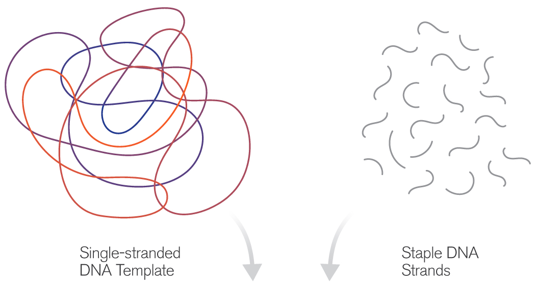
The basic idea of DNA origami is to use a length of single-stranded DNA as a scaffold for the desired shape. Base-pairing of complementary nucleotides causes the form to fold and self-assemble. The process is guided by the addition of shorter “staple strands,” which act to help fold the scaffold and to hold the resulting structure together. Various imaging technologies are used to observe the tiny structures, including fluorescence-, electron- and atomic force microscopy.


DNA origami originally produced nanoarchitectures of purely aesthetic interest, but refinements of the technique have opened the door to a new range of exciting applications including molecular cages for the encapsulation of molecules, enzyme immobilization and catalysis, chemical and biological sensing tools, drug delivery mechanisms, and molecular computing devices.

The technique described in the new study takes this approach a step further, allowing researchers to overcome local symmetry restrictions, creating wireframe architectures with higher order arbitrariness and complexity. Here, each line segment and vertex is individually designed and controlled. The number of arms emanating from each vertex may be varied from 2 to 10 and the precise angles between adjacent arms can be modified.

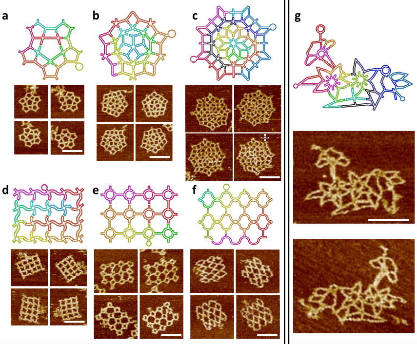
The scaffold folding path and representative AFM images for intricate 2D patterns. (a) A star-shape pattern without translational symmetry. (a) A Penrose tiling. (c) An 8-fold quasicrystalline pattern. (d-f) Three curved structures. (d) A waving grid. (e) A sphere array. (f) A fishnet. (g) A flower-and-bird pattern. All scale bars are 100 nm. Two scaffolds (one colorful and one black-blue) are used in c and g. (credit: Fei Zhang et al./Nature Nanotechnology)

In the current study, the method was first applied to symmetrical, regularly repeating polygonal designs, including hexagonal, square and triangular tiling geometries. Such common designs are known as tessellation patterns. A clever strategy involving a series of bridges and loops was used to properly route the scaffold strand, allowing it to pass through the entire structure, touching all lines of the wireframe once and only once. Staple strands were then applied to complete the designs.

In subsequent stages, the researchers created more complex wireframe structures, without the local translational symmetry found in the tessellation patterns. Three such patterns were made, including a star shape, a 5-fold Penrose tile and an 8-fold quasicrystalline pattern. (Quasicrystals are structures that are highly ordered but non-periodic. Such patterns can continuously fill available space, but are not translationally symmetric.)

Loop structures inserted into staple strands and unpaired nucleotides at the vertex points of the scaffold strands were also used, allowing researchers to perform precision modifications to the angles of junction arms.

The new design rules were next tested with the assembly of increasingly complex nanostructures, involving vertices ranging from 2 to 10 arms, with many different angles and curvatures involved, including a complex pattern of birds and flowers. The accuracy of the design was subsequently confirmed by AFM imaging, proving that the method could successfully yield highly sophisticated wireframe DNA nanostructures.

3D wire-frame Archimedean solid structures. (a) A 3D model of an Archimedean solid cuboctahedron with 12 vertices and 24 edges. Each vertex is a 4 Å~ 4 junction, and each edge is a 14-turn long double DNA duplex. (b) Left: Models showing possible conformations of the structure when deposited on mica surface; Right: the corresponding AFM images. (c) The reconfiguration between 3D and 2D can be realized by strand displacement by adding fuel and set strands. Top: reconfiguration schematics, Bottom: AFM images showing the transition. All scale bars in AFM images are 100 nm. (d) A 3D model of snub cube with 24 vertices and 60 edges. Each vertex is 5 Å~ 4 junction, and each edge is a 5-turn double DNA duplex. (e) Three views of the DNA snub cube from the design model (top of page). (credit: Fei Zhang et al./Nature Nanotechnology)

The method was then adapted to produce a number of 3D structures as well, including a cuboctahedron, and another Archimedian solid known as a snub cube — a structure with 60 edges, 24 vertices and 38 faces, including 6 squares and 32 equilateral triangles.

The authors stress that the new design innovations described can be used to compose and construct any imaginable wireframe nanostructure— a significant advancement for the burgeoning field.

On the horizon, nanoscale structures may one day be marshaled to hunt cancer cells in the body or act as robot assembly lines for the design of new drugs.


Abstract of Complex wireframe DNA origami nanostructures with multi-arm junction vertices

Structural DNA nanotechnology and the DNA origami technique, in particular, have provided a range of spatially addressable two- and three-dimensional nanostructures. These structures are, however, typically formed of tightly packed parallel helices. The development of wireframe structures should allow the creation of novel designs with unique functionalities, but engineering complex wireframe architectures with arbitrarily designed connections between selected vertices in three-dimensional space remains a challenge. Here, we report a design strategy for fabricating finite-size wireframe DNA nanostructures with high complexity and programmability. In our approach, the vertices are represented by n × 4 multi-arm junctions (n = 2–10) with controlled angles, and the lines are represented by antiparallel DNA crossover tiles of variable lengths. Scaffold strands are used to integrate the vertices and lines into fully assembled structures displaying intricate architectures. To demonstrate the versatility of the technique, a series of two-dimensional designs including quasi-crystalline patterns and curvilinear arrays or variable curvatures, and three-dimensional designs including a complex snub cube and a reconfigurable Archimedean solid were constructed.

Phosphorene could lead to ultrathin solar cells


Australian National University | Sticky tape the key to ultrathin solar cells

Scientists at Australian National University (ANU) have used simple transparent sticky (aka “Scotch”) tape to create single-atom-thick layers of phosphorene from “black phosphorus,” a black crystalline form of phosphorus similar to graphite (which is used to create graphene).

Unlike graphene, phosphorene is a natural semiconductor that can be switched on and off, like silicon, as KurzweilAI has reported. “Because phosphorene is so thin and light, it creates possibilities for making lots of interesting devices, such as LEDs or solar cells,” said lead researcher Yuerui (Larry) Lu, PhD, from ANU College of Engineering and Computer Science.

Properties that vary with layer thickness

Phosphorene is a thinner and lighter semiconductor than silicon, and it has unusual light emission properties that vary widely with the thickness of the layers, which enables more flexibility for manufacturing. “This property has never been reported before in any other material,” said Lu.

Schematic of the “puckered honeycomb” crystal structure of black phosphorus (credit: Vahid Tayari/McGill University)

“By changing the number of layers [peeled off] we can tightly control the band gap, which determines the material’s properties, such as the color of LED it would make.* “You can see quite clearly under the microscope the different colors of the sample, which tells you how many layers are there,” said Dr Lu.

The study was recently described in an open-access paper in the Nature journal Light: Science and Applications.

* Lu’s team found the optical gap for monolayer (single-layer) phosphorene was 1.75 electron volts, corresponding to red light of a wavelength of 700 nanometers. As more layers were added, the optical gap decreased. For instance, for five layers, the optical gap value was 0.8 electron volts, a infrared wavelength of 1550 nanometres. For very thick layers, the value was around 0.3 electron volts, a mid-infrared wavelength of around 3.5 microns.


Abstract of Optical tuning of exciton and trion emissions in monolayer phosphorene

Monolayer phosphorene provides a unique two-dimensional (2D) platform to investigate the fundamental dynamics of excitons and trions (charged excitons) in reduced dimensions. However, owing to its high instability, unambiguous identification of monolayer phosphorene has been elusive. Consequently, many important fundamental properties, such as exciton dynamics, remain underexplored. We report a rapid, noninvasive, and highly accurate approach based on optical interferometry to determine the layer number of phosphorene, and confirm the results with reliable photoluminescence measurements. Furthermore, we successfully probed the dynamics of excitons and trions in monolayer phosphorene by controlling the photo-carrier injection in a relatively low excitation power range. Based on our measured optical gap and the previously measured electronic energy gap, we determined the exciton binding energy to be ~0.3 eV for the monolayer phosphorene on SiO2/Si substrate, which agrees well with theoretical predictions. A huge trion binding energy of ~100 meV was first observed in monolayer phosphorene, which is around five times higher than that in transition metal dichalcogenide (TMD) monolayer semiconductor, such as MoS2. The carrier lifetime of exciton emission in monolayer phosphorene was measured to be ~220 ps, which is comparable to those in other 2D TMD semiconductors. Our results open new avenues for exploring fundamental phenomena and novel optoelectronic applications using monolayer phosphorene.