3D-printing basic electronic components

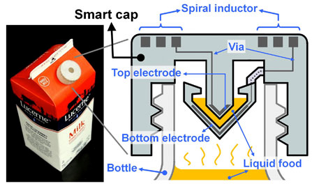
UC Berkeley engineers created a “smart cap” using 3-D-printed plastic with embedded electronics to wirelessly monitor the freshness of milk (credit: Photo and schematic by Sung-Yueh Wu)

UC Berkeley engineers, in collaboration with colleagues at Taiwan’s National Chiao Tung University, have developed a 3D printing process for creating basic electronic components, such as resistors, inductors, capacitors, and integrated wireless electrical sensing systems.

As a test, they printed a wireless “smart cap” for a milk carton that detected signs of spoilage using embedded sensors.

The findings were published Monday, July 20, in a new open-access journal in the Nature Publishing Group called Microsystems & Nanoengineering.

“Our paper describes the first demonstration of 3-D printing for working basic electrical components, as well as a working wireless sensor,” said senior author Liwei Lin, a professor of mechanical engineering and co-director of the Berkeley Sensor and Actuator Center.“One day, people may simply download 3D-printing files from the Internet with customized shapes and colors and print out useful devices at home.”

Engineers created a range of 3-D-printed electrical components, including an electrical resistor, inductor, capacitor and an LC tank (integrated inductor-capacitor system) (the penny is used for scale), shown here before removal of wax (credit: Photo by Sung-Yueh Wu)

The researchers started by printing polymers and wax. They then removed the wax, leaving hollow tubes into which liquid metal —- in their experiments they used silver — was injected and then cured.

The shape and design of the metal determined the function of different electrical components. For instance, thin wires acted as resistors, and flat plates were made into capacitors.

To demonstrate their use, the researchers integrated the electronic components into a plastic milk carton cap to monitor signs of spoilage. The “smart cap” was fitted with a capacitor and an inductor to form a resonant circuit. A quick flip of the carton allowed a bit of milk to get trapped in the cap’s capacitor gap, and the entire carton was then left unopened at room temperature (about 71.6 degrees Fahrenheit) for 36 hours.
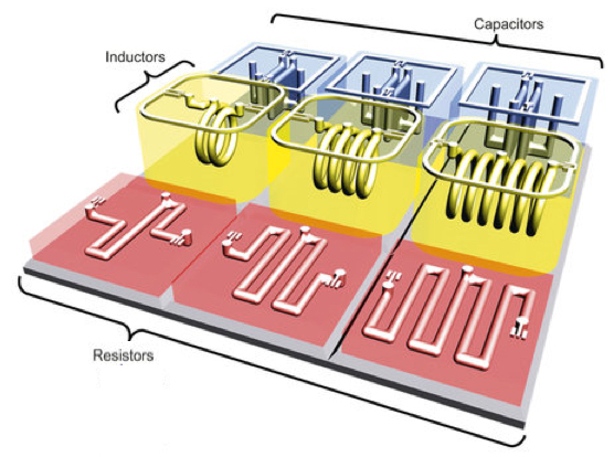
3D-printed components (credit: Sung-Yueh Wu et al./Microsystems & Nanoengineering)

The circuit could detect the changes in electrical signals that accompany increased levels of bacteria. The researchers periodically monitored the changes with a wireless radio-frequency probe at the start of the experiment and every 12 hours thereafter, up to 36 hours. The property of milk changes gradually as it degrades, leading to variations in its electrical characteristics*.

Those changes were detected wirelessly using the smart cap, which found that the peak vibration frequency of the room-temperature milk dropped by 4.3 percent after 36 hours. In comparison, a carton of milk kept in refrigeration at 39.2 degrees Fahrenheit saw a relatively minor 0.12 percent shift in frequency over the same time period.

Cheap DIY electronic circuits 

“This 3D-printing technology could eventually make electronic circuits cheap enough to be added to packaging to provide food safety alerts for consumers,” said Lin. “You could imagine a scenario where you can use your cellphone to check the freshness of food while it’s still on the store shelves.”

As 3D printers become cheaper and better, the options for electronics will expand, said Lin, though he does not think people will be printing out their own smartphones or computers anytime soon.

“That would be very difficult because of the extremely small size of modern electronics,” he said. “It might also not be practical in terms of price since current integrated circuits are made by batch fabrication to keep costs low. Instead, I see 3D-printed microelectronic devices as very promising for systems that would benefit from customization.”

Lin said his lab is working on developing this technology for health applications, such as implantable devices with embedded transducers that can monitor blood pressure, muscle strain and drug concentrations.

* As the trapped milk hardened, the dielectric constant increased, increasing the capacitance and thus decreasing the frequency.


Abstract of 3D-printed microelectronics for integrated circuitry and passive wireless sensors

Three-dimensional (3D) additive manufacturing techniques have been utilized to make 3D electrical components, such as resistors, capacitors, and inductors, as well as circuits and passive wireless sensors. Using the fused deposition modeling technology and a multiple-nozzle system with a printing resolution of 30 μm, 3D structures with both supporting and sacrificial structures are constructed. After removing the sacrificial materials, suspensions with silver particles are injected subsequently solidified to form metallic elements/interconnects. The prototype results show good characteristics of fabricated 3D microelectronics components, including an inductor–capacitor-resonant tank circuitry with a resonance frequency at 0.53 GHz. A 3D “smart cap” with an embedded inductor–capacitor tank as the wireless passive sensor was demonstrated to monitor the quality of liquid food (e.g., milk and juice) wirelessly. The result shows a 4.3% resonance frequency shift from milk stored in the room temperature environment for 36 h. This work establishes an innovative approach to construct arbitrary 3D systems with embedded electrical structures as integrated circuitry for various applications, including the demonstrated passive wireless sensors.

Metal foams found to excel in shielding X-rays, gamma rays, neutron radiation

Lightweight composite metal foams like this one have been found effective at blocking X-rays, gamma rays and neutron radiation, and are capable of absorbing the energy of high impact collisions — holding promise for use in nuclear safety, space exploration, and medical technology applications (credit: Afsaneh Rabiei, North Carolina State University)

North Carolina State University researchers have found that lightweight composite metal foams they had developed are effective at blocking X-rays, gamma rays, and neutron radiation, and are capable of absorbing the energy of high-impact collisions. The finding holds promise for use in nuclear power plants, space exploration, and CT-scanner shielding.

“This work means there’s an opportunity to use composite metal foam to develop safer systems for transporting nuclear waste, more efficient designs for spacecraft and nuclear structures, and new shielding for use in CT scanners,” says

Afsaneh Rabiei, a professor of mechanical and aerospace engineering at NC State, first developed the strong, lightweight metal foam made of steel, tungsten, and and vanadium for use in transportation and military applications. But she wanted to determine whether the foam could be used for nuclear or space exploration applications — could it provide structural support and protect against high impacts while providing shielding against various forms of radiation?

So she and her colleagues conducted multiple tests to see how effective it was at blocking X-rays, gamma rays, and neutron radiation. She then compared the material’s performance to the performance of bulk materials that are currently used in shielding applications. The comparison was made using samples of the same “areal” density – meaning that each sample had the same weight, but varied in volume.

Better than lead and non-toxic

The researchers found that the high-Z foam was comparable to bulk materials at blocking high-energy gamma rays, but was much better than bulk materials — even bulk steel — at blocking low-energy gamma rays; it outperformed other materials at blocking neutron radiation; and was better than most materials at blocking X-rays. It was not quite as effective as lead, but with the advantages of  being lightweight and more environmentally friendly.

“However, we are working to modify the composition of the metal foam to be even more effective than lead at blocking X-rays, and our early results are promising,” Rabiei says. “And our foams have the advantage of being non-toxic, which means that they are easier to manufacture and recycle. In addition, the extraordinary mechanical and thermal properties of composite metal foams, and their energy absorption capabilities, make the material a good candidate for various nuclear structural applications.”

The research paper was published in Radiation Physics and Chemistry. It was supported by DOE’s Office of Nuclear Energy under Nuclear Energy University Program.


Abstract of Attenuation efficiency of X-ray and comparison to gamma ray and neutrons in composite metal foams

Steel-steel composite metal foams (S-S CMFs) and Aluminum-steel composite metal foams (Al-S CMFs) with various sphere sizes and matrix materials were manufactured and investigated for nuclear and radiation environments applications. 316 L stainless steel, high-speed T15 steel and aluminum materials were used as the matrix material together with 2, 4 and 5.2 mm steel hollow spheres to manufacture various types of composite metal foams (CMFs). High-speed T15 steel is selected due to its high tungsten and vanadium concentration (both high-Z elements) to further improve the shielding efficiency of CMFs. This new type of S-S CMF is called High-Z steel-steel composite metal foam (HZ S-S CMF). Radiation shielding efficiency of all types of CMFs was explored for the attenuation of X-ray, gamma ray and neutron. The experimental results were compared with pure lead and Aluminum A356, and verified theoretically through XCOM and Monte Carlo Z-particle Transport Code (MCNP). It was observed that the radiation shielding effectiveness of CMFs is relatively independent of sphere sizes as long as the ratio of sphere-wall thickness to its outer-diameter stays constant. However, the smaller spheres seem to be more efficient in general due to the fine fluctuation in the gray value profile of their 2D Micro-CT images. S-S CMFs and Al-S CMFs are respectively 275% and 145% more effective for X-ray attenuation than Aluminum A356. Compared to pure lead, CMFs show adequate attenuation with additional advantages of being lightweight and more environmentally friendly. The mechanical performance of HZ S-S CMFs under quasi-static compression was compared to that of other classes of S-S CMF. It is observed that the addition of high-Z elements to the matrix of CMFs improved their shielding against X-rays, low energy gamma rays and neutrons, while maintained their low density, high mechanical properties and high-energy absorption capability.

Why ‘white graphene’ structures are cool

A 3-D structure of hexagonal boron nitride sheets and boron nitride nanotubes could be a tunable material to control heat in electronics, according to researchers at Rice University (credit: Shahsavari Group/Rice University)


Three-dimensional structures of boron nitride are a viable candidate as a tunable material to keep electronics cool, according to scientists at Rice University researchers Rouzbeh Shahsavari and Navid Sakhavand.

Their work appears this month in the American Chemical Society journal Applied Materials and Interfaces.

In its two-dimensional form, hexagonal boron nitride (h-BN), aka white graphene, looks just like the atom-thick form of carbon known as graphene. One difference: h-BN is a natural insulator, where perfect graphene presents no barrier to electricity (is a natural electrical conductor).

But like graphene, h-BN is a also a good conductor of heat, which can be quantified in the form of phonons. (Technically, a phonon is a “quasiparticle” in a collective excitation of atoms.)

“Typically in all electronics, it is highly desired to get heat out of the system as quickly and efficiently as possible,” he said. “One of the drawbacks in electronics, especially when you have layered materials on a substrate, is that heat moves very quickly in one direction, along a conductive plane, but not so good from layer to layer. Multiple stacked graphene layers is a good example of this.”

Heat moves ballistically across flat planes of boron nitride, too, but the Rice simulations showed that 3-D structures of h-BN planes connected by boron nitride nanotubes would be able to move phonons in all directions, whether in-plane or across planes, Shahsavari said.

Phonon flows

The researchers calculated how phonons would flow across four such structures with nanotubes of various lengths and densities. They found the junctions of pillars and planes significantly slowed down the flow of phonons from layer to layer, Shahsavari said. Both the length and density of the pillars had an effect on the heat flow: more and/or shorter pillars slowed conduction, while longer pillars presented fewer barriers and thus sped things along.

Researchers have already made graphene/carbon nanotube junctions, but Shahsavari believes such junctions for boron nitride materials could be just as promising. “Given the insulating properties of boron nitride, they can enable and complement the creation of 3-D, graphene-based nanoelectronics,” Shahsavari said.

“This type of 3-D thermal-management system can open up opportunities for thermal switches, or thermal rectifiers, where the heat flowing in one direction can be different than the reverse direction. This can be done by changing the shape of the material, or changing its mass — say one side is heavier than the other — to create a switch. The heat would always prefer to go one way, but in the reverse direction it would be slower.”


Abstract of Dimensional Crossover of Thermal Transport in Hybrid Boron Nitride Nanostructures

Although Boron Nitride nanotubes (BNNT) and hexagonal-BN (h-BN) are superb one-dimensional (1D) and 2D thermal conductors respectively, bringing this quality into 3D remain elusive. Here, we focus on Pillared Boron Nitride (PBN) as a class of 3D BN allotropes and demonstrate how the junctions, pillar length and pillar distance control phonon scattering in PBN and impart tailorable thermal conductivity in 3D. Using reverse non equilibrium molecular dynamics simulations, our results indicate that while a clear phonon scattering at the junctions accounts for the lower thermal conductivity of PBN compared to its parent BNNT and h-BN allotropes, it acts as an effective design tool and provides 3D thermo-mutable features that are absent in the parent structures. Propelled by the junction spacing, while one geometrical parameter, e.g., pillar length, controls the thermal transport along the out-of-plane direction of PBN, the other parameter, e.g., pillar distance, dictates the gross cross-sectional area, which is key for design of 3D thermal management systems. Furthermore, the junctions have a more pronounced effect in creating a Kapitza effect in the out-of-plane direction, due to the change in dimensionality of the phonon transport. This work is the first report on thermo-mutable properties of hybrid BN allotropes and can potentially impact thermal management of other hybrid 3D BN architectures.

Nanospheres safely deliver high chemotherapy doses to attack tumors

Cancer tumors secrete enzymes are triggered by peptide coatings (blue) to slice the coatings open, safely delivering an anti-cancer drug (red) (credit: Cassandra E. Callmann et al./Advanced Materials)

Scientists have engineered a drug delivery system that uses specially designed nanoparticles that release drugs in the presence of a specific enzymes — the very ones that enable cancers to metastasize.

“We can start with a small molecule and build that into a nanoscale carrier that can seek out a tumor and deliver a payload of drug,” said Cassandra Callmann, a graduate student in chemistry and biochemistry at the University of California, San Diego, and first author of the report published in the journal Advanced Materials July 14.

Trojan-horse strategy

The system takes advantage of a class of enzymes called matrix metalloproteinases (MMPs) that many cancers make in abundance. MMPs normally chew through through the body’s membranes, allowing cancer cells to escape to metastasize (colonize other regions of the body), often with deadly consequences.

Trojan-horse strategy: an anti-cancer drug (Paclitaxel) and a peptide self-assemble into nanoparticles. Released at the cancer location, the peptide shell triggers cancer-cell enzymes (MMP) to rip apart the nanoparticle shell, releasing the drug (credit: Cassandra E. Callmann/Advanced Materials)

So Callmann created tiny spheres packed with the anti-cancer drug paclitaxel (also known by the trade names Taxol and Onxal) and coated with a peptide shell. When MMPs sense the peptide, they go pitbull on it, tearing up that shell, and releasing the drug. The shell fragments form a ragged mesh that holds the drug molecules near the tumor.

The work, led by Nathan Gianneschi a professor of chemistry and biochemisty at UC San Diego, builds on his group’s earlier success using a similar strategy to mark tumors for both diagnosis and precise surgical removal.

16 times higher anti-cancer dose safely administered

To package the drug into the spheres, Callmann had to add chemical handles. As it turns out, a group of atoms essential to the drug molecule’s effectiveness, and also toxicity, made for a good attachment point. That means the drug was safely inactivated as it flowed through the circulatory system until it reached the tumor.

The protection allowed the researchers to safely give a dose 16 times higher than they could with the formulation now used in cancer clinics, in a test in mice with grafted in fibrosarcoma tumors.

In additional preliminary tests, Callmann and colleagues were able to halt the growth of the tumors for a least two weeks, using a single lower dose of the drug. In mice treated with the nanoparticles that were coated with peptides that are instead impervious to MMPs or given saline, the tumors grew to lethal sizes within that time.

Gianneschi says they will broaden their approach to create delivery systems for other diagnostic and therapeutic molecules. “This kind of platform is not specific to paclitaxel. We’ll test this in other models — with other classes of drug and in mice with a cancer that mimics metastatic breast cancer, for example.”

They’ll also continue to modify the shell, to provide even greater protection and avoid uptake by organs such as liver, spleen and kidneys, he said. “We want to open up this therapeutic window.”


Abstract of Therapeutic Enzyme-Responsive Nanoparticles for Targeted Delivery and Accumulation in Tumors

An enzyme-responsive, paclitaxel-loaded nanoparticle is described and assessed in vivo in a human fibrosarcoma murine xenograft. This work represents a proof-of-concept study demonstrating the utility of enzyme-responsive nanoscale drug carriers capable of targeted accumulation and retention in tumor tissue in response to overexpressed endogenous enzymes.

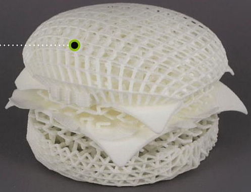
3-D printed food

(credit: excerpt from cover of Fabricated: The New World of 3D Printing by Tod Lipson)

3D printers could revolutionize food processing in the next 10 to 20 years, said Hod Lipson, Ph.D., a professor of engineering at Columbia University, speaking at IFT15: Where Science Feeds Innovation.

“The technology is getting faster, cheaper, and better by the minute. Food printing could be the killer app for 3D printing.”

Lipson, who is co-author of Fabricated: The New World of 3D Printing, said 3D printing is a good fit for the food industry because it allows manufacturers to bring complexity and variety to consumers at a low cost.

For example, Lipson said, users could choose from a large online database of recipes, put a cartridge with the ingredients into their 3D printer at home, and it would create the dish just for that person. The user could customize it to include extra nutrients or replace one ingredient with another.

Mary Scerra, food technologist at the U.S. Army Natick Soldier Research, Development and Engineering Center (NSRDEC) said that by 2025 or 2030, the military envisions using 3D printing to customize meals for soldiers that “taste good [seriously?], are nutrient-dense, and could be tailored to a soldier’s particular needs.”

Using graphene-based film for efficient cooling of electronics

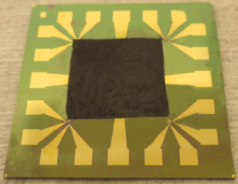
Graphene-based film on a hot electronic component (credit: Johan Liu)

A method for efficiently cooling electronics using graphene-based film — with a thermal conductivity capacity four times higher than copper — has been developed by researchers at Chalmers University of Technology. The film can be attached to computer chips and other silicon-based electronic components.

Electronic systems available today accumulate a great deal of heat, mostly due to the ever-increasing demand on functionality. Getting rid of excess heat in efficient ways is needed for chip lifespan and reduction in energy usage.

A research team led by Johan Liu, a professor at Chalmers University of Technology, originally found that graphene can have a cooling effect on silicon-based electronics, but that it’s not efficient because it’s limited to a few layers of graphene atoms. “When you try to add more layers of graphene, the graphene will no longer adhere to the surface, since the adhesion is [due to] weak van der Waals bonds,” he said.

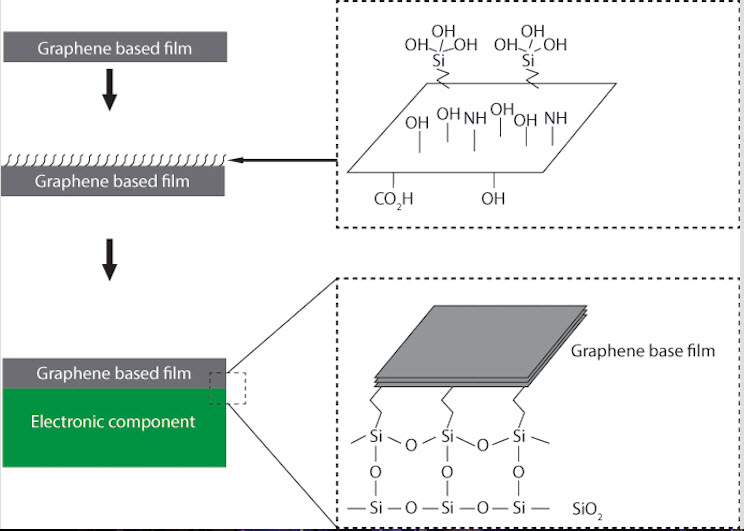
Silane coupling between graphene and silicon. After heating and hydrolysis of (3-Aminopropyl) triethoxysilane (APTES) molecules (top right), silane coupling (bottom right) is created, providing mechanical strength and good thermal pathways (credit: Johan Liu)

The researchers solved that by creating strong covalent bonds between the graphene film and the surface. The stronger bonds result from adding (3-Aminopropyl) triethoxysilane (APTES) molecules to the film. Heating and hydrolysis then creates silane bonds between the graphene and the electronic component, doubling thermal conductivity.

“Increased thermal capacity could lead to several new [cooling] applications for graphene,” says Liu, including LEDs, lasers, and radio frequency components.


Abstract of Improved Heat Spreading Performance of Functionalized Graphene in Microelectronic Device Application

It is demonstrated that a graphene-based film (GBF) functionalized with silane molecules strongly enhances thermal performance. The resistance temperature detector results show that the inclusion of silane molecules doubles the heat spreading ability. Furthermore, molecular dynamics simulations show that the thermal conductivity (κ) of the GBF increased by 15%–56% with respect to the number density of molecules compared to that with the nonfunctionalized graphene substrate. This increase in κ is attributed to the enhanced in-plane heat conduction of the GBF, resulting from the simultaneous increase of the thermal resistance between the GBF and the functionalized substrate limiting cross-plane phonon scattering. Enhancement of the thermal performance by inserting silane-functionalized molecules is important for the development of next-generation electronic devices and proposed application of GBFs for thermal management.

How to visually determine thickness at one-nanometer resolution by eye

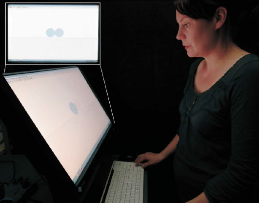
Research shows how accurately a naked human eye can determine the thickness of thin-films from the observed color (credit: Sandy Peterhänsel et al./Optica)

European scientists have taught volunteers in an experiment how to determine the thickness of a titanium dioxide thin film only a few nanometers thick by simply observing the color it presents under under highly controlled, precise lighting conditions, according to Sandy Peterhänsel, University of Stuttgart, Germany and principal author of an open-access paper in the journal Optica.

The optical properties of thin films are the result of light interacting with their surfaces to produce a wide range of colors. This is the same phenomenon that produces scintillating colors in soap bubble and oil films on water.

The specific colors produced by this process depend strongly on the composition of the material, its thickness, and the properties of the incoming light. This high sensitivity to both the material and thickness has sometimes been used by skilled engineers to quickly estimate the thickness of films down to a level of approximately 10–20 nanometers. Could someone see a thinner film?

The experiment

Composed photo of all samples (bottom row) and adjusted color fields (top row). Residual defects of the samples can be seen at the edges of some samples. (credit: Sandy Peterhänsel et al./Optica)

The researchers decided to find out. The experiment setup was simple: a series of thin films of titanium dioxide were manufactured one layer at a time by atomic deposition. While time consuming, this method enabled the researchers to carefully control the thickness of the samples.

The samples were then placed on a LCD monitor that was set to display a pure white color, with the exception of a colored reference area that could be calibrated to match the apparent surface colors of the thin films with various thicknesses.

The color of the reference field was then changed by the test subject until it perfectly matched the reference sample: correctly identifying the color meant they also correctly determined its thickness. This could be done in as little as two minutes, and for some samples and test subjects their estimated thickness differed only by one-to-three nanometers from the actual value measured by conventional means. This level of precision is far beyond normal human vision.

Compared to traditional automated methods of determining the thickness of a thin film, which can take five to ten minutes per sample using some techniques, the human eye performance compared very favorably.

The researchers speculate that it may be possible to detect even finer variations if other control factors are put in place. “People often underestimate human senses and their value in engineering and science. This experiment demonstrates that our natural born vision can achieve exceptional tasks that we normally would only assign to expensive and sophisticated machinery,” concludes Peterhänsel.


Abstract of Human color vision provides nanoscale accuracy in thin-film thickness characterization

We study how accurately a naked human eye can determine the thickness of thin films from the observed color. Our approach is based on a color-matching experiment between thin-film samples and a simulated color field shown on an LCD monitor. We found that the human color observation provides an extremely accurate evaluation of the film thickness, and is comparable to sophisticated instrumental methods. The remaining color differences for the matched color pairs are close to the literature value for the smallest visually perceivable color difference.

A graphene-based molecule sensor

Shining infrared light on a graphene surface makes surface electrons oscillate in different ways that identify the specific molecule attached to the surface (EPFL/Miguel Spuch /Daniel Rodrigo )

European scientists have harnessed graphene’s unique optical and electronic properties to develop a highly sensitive sensor to detect molecules such as proteins and drugs — one of the first such applications of graphene.

The results are described in an article appearing in the latest edition of the journal Science.

The researchers at EPFL’s Bionanophotonic Systems Laboratory (BIOS) and the Institute of Photonic Sciences (ICFO, Spain) used graphene to improve on a molecule-detection method called infrared absorption spectroscopy, which uses infrared light is used to excite the molecules. Each type of molecule absorbs differently across the spectrum, creating a signature that can be recognized.

This method is not effective, however, in detecting molecules that are under 10 nanometers in size (such as proteins), because the size of the mid-infrared wavelengths used are huge in comparison — 2 to 6 micrometers (2,000 to 6,000 nanometers).

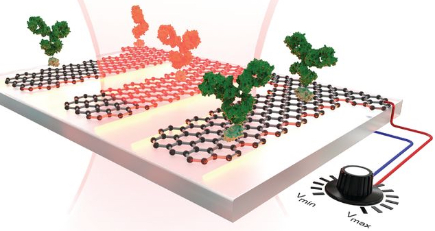
Conceptual view of the graphene biosensor. An infrared beam excites a plasmon resonance across the graphene nanoribbons. Protein sensing is achieved by changing the voltage applied to the graphene and detecting a plasmon resonance spectral shift accompanied by narrow dips corresponding to the molecular vibration bands of the protein. (credit: Daniel Rodrigo et al./Science)

Resonant vibrations

With the new graphene method, the target proteins to be analyzed are attached to the graphene surface. “We pattern nanostructures on the graphene surface by bombarding it with electron beams and etching it with oxygen ions,” said Daniel Rodrigo, co-author of the publication. “When the light arrives, the electrons in graphene nanostructures begin to oscillate. This phenomenon, known as ‘localized surface plasmon resonance,’ serves to concentrate light into tiny spots, which are comparable with the [tiny] dimensions of the target molecules. It is then possible to detect nanometric structures.”

This process can also reveal the nature of the bonds connecting the atoms that the molecule is composed of. When a molecule vibrates, it does so in a range of frequencies, which are generated by the bonds connecting the different atoms. To detect these frequencies,  the researchers “tuned” the graphene to different frequencies by applying voltage, which is not possible with current sensors. Making graphene’s electrons oscillate in different ways makes it possible to “read” all the vibrations of the molecule on its surface. “It gave us a full picture of the molecule,” said co-author Hatice Altug.

According to the researchers, this simple method shows that it is possible to conduct a complex analysis using only one device, while it normally requires many different ones, and without stressing or modifying the biological sample. “The method should also work for polymers, and many other substances,” she added.


Abstract of Mid-infrared plasmonic biosensing with graphene

Infrared spectroscopy is the technique of choice for chemical identification of biomolecules through their vibrational fingerprints. However, infrared light interacts poorly with nanometric-size molecules. We exploit the unique electro-optical properties of graphene to demonstrate a high-sensitivity tunable plasmonic biosensor for chemically specific label-free detection of protein monolayers. The plasmon resonance of nanostructured graphene is dynamically tuned to selectively probe the protein at different frequencies and extract its complex refractive index. Additionally, the extreme spatial light confinement in graphene—up to two orders of magnitude higher than in metals—produces an unprecedentedly high overlap with nanometric biomolecules, enabling superior sensitivity in the detection of their refractive index and vibrational fingerprints. The combination of tunable spectral selectivity and enhanced sensitivity of graphene opens exciting prospects for biosensing.

Creating DNA-based nanostructures without water

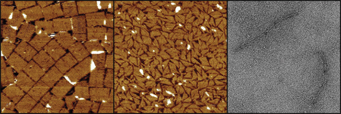
Three different DNA nanostructures assembled at room temperature in water-free glycholine (left) and in 75 percent glycholine-water mixture (center and right). The structures are (from left to right) a tall rectangle two-dimensional DNA origami, a triangle made of single-stranded tails, and a six-helix bundle three-dimensional DNA origami (credit: Isaac Gállego).

Researchers at the Georgia Institute of Technology have discovered an new process for assembling DNA nanostructures in a water-free solvent, which may allow for fabricating more complex nanoscale structures — especially, nanoelectronic chips based on DNA.

Scientists have been using DNA to construct sophisticated new structures from nanoparticles (such as a recent development at Brookhaven National Labs reported by KurzweilAI May 26), but the use of DNA has required a water-based environment. That’s because DNA naturally functions inside the watery environment of living cells. However, the use of water limited the types of structures that are possible.

The viscosity of a new solvent used for assembling DNA nanostructures (credit: Rob Felt)

In addition, the Georgia Tech researchers discovered that, paradoxically, adding a small amount of water to their water-free solvent during the assembly process (and removing it later) increases the assembly rate. It could also allow for even more complex structures, by reducing the problem of DNA becoming trapped in unintended structures by aggregation (clumping).

The new solvent they used is known as glycholine, a mixture of glycerol (used for sweetening and preserving food) and choline chloride, but the researchers are exploring other materials.

The solvent system could improve the combined use of metallic nanoparticles and DNA based materials at room temperature. The solvent’s low volatility could also allow for storage of assembled DNA structures without the concern that a water-based medium would dry out.

The research on water-free solvents grew out of Georgia Tech researchers’ studies in the origins of life. They wondered if the molecules necessary for life, such as the ancestor of DNA, could have developed in a water-free solution. In some cases, they found, the chemistry necessary to make the molecules of life would be much easier without water being present.

Sponsored by the National Science Foundation and NASA, the research will be published as the cover story in Volume 54, Issue 23 of the journal Angewandte Chemie International Edition.

* The assembly rate of DNA nanostructures can be very slow, and depends strongly on temperature. Raising the temperature increases this rate, but temperatures that are too high can cause the DNA structures to fall apart. The solvent system developed at Georgia Tech adds a new level of control over DNA assembly. DNA structures assemble at lower temperatures in this solvent, and adding water can adjust the solvent’s viscosity (resistance to flow), which allows for faster assembly compared to the water-free version of the solvent.


Abstract of Folding and Imaging of DNA Nanostructures in Anhydrous and Hydrated Deep-Eutectic Solvents

There is great interest in DNA nanotechnology, but its use has been limited to aqueous or substantially hydrated media. The first assembly of a DNA nanostructure in a water-free solvent, namely a low-volatility biocompatible deep-eutectic solvent composed of a 4:1 mixture of glycerol and choline chloride (glycholine), is now described. Glycholine allows for the folding of a two-dimensional DNA origami at 20 °C in six days, whereas in hydrated glycholine, folding is accelerated (≤3 h). Moreover, a three-dimensional DNA origami and a DNA tail system can be folded in hydrated glycholine under isothermal conditions. Glycholine apparently reduces the kinetic traps encountered during folding in aqueous solvent. Furthermore, folded structures can be transferred between aqueous solvent and glycholine. It is anticipated that glycholine and similar solvents will allow for the creation of functional DNA structures of greater complexity by providing a milieu with tunable properties that can be optimized for a range of applications and nanostructures.

Dynamically reprogramming matter

Various types of reprogramming DNA strands can be used to selectively trigger transformations to radically different phases (configurations) of the initial particle structure (credit: Brookhaven National Laboratory)

Scientists at the U.S. Department of Energy’s Brookhaven National Laboratory have developed the capability of creating dynamic nanomaterials — ones whose structure and associated properties can be switched, on-demand. In a paper appearing in Nature Materials, they describe a way to selectively rearrange nanoparticles in three-dimensional arrays to produce different configurations, or “phases,” from the same nano-components.

“One of the goals in nanoparticle self-assembly has been to create structures by design,” said Oleg Gang, who led the work at Brookhaven’s Center for Functional Nanomaterials (CFN), a DOE Office of Science User Facility. “Until now, most of the structures we’ve built have been static.” KurzweilAI covered that development in a previous article, “Creating complex structures using DNA origami and nanoparticles.”

The new advance in nanoscale engineering builds on that previous work in developing ways to get nanoparticles to self-assemble into complex composite arrays, including linking them together with tethers constructed of complementary strands of synthetic DNA.

“We know that properties of materials built from nanoparticles are strongly dependent on their arrangements,” said Gang. “Previously, we’ve even been able to manipulate optical properties by shortening or lengthening the DNA tethers. But that approach does not permit us to achieve a global reorganization of the entire structure once it’s already built.”

DNA-directed rearrangement

“Now we are trying to achieve an even more ambitious goal,” reveal Gang: “Making materials that can transform so we can take advantage of properties that emerge with the particles’ rearrangements.”

The ability to direct particle rearrangements, or phase changes, will allow the scientists to choose the desired properties — say, the material’s response to light or a magnetic field — and switch them whenever needed. Such phase-changing materials could lead to radical new applications, such as dynamic energy-harvesting or responsive optical materials.

Injecting different kinds of reprogramming DNA strands can change the interparticle interactions in different ways depending on whether the new strands increase attraction or repulsion, or there’s a combination of these forces between particles (credit: Brookhaven National Laboratory)

In the new approach, the reprogramming DNA strands adhere to open binding sites on the already assembled nanoparticles. These strands exert additional forces on the linked-up nanoparticles.

“By introducing different types of reprogramming DNA strands, we modify the DNA shells surrounding the nanoparticles,” explained CFN postdoctoral fellow Yugang Zhang, the lead author on the paper. “Altering these shells can selectively shift the particle-particle interactions, either by increasing both attraction and repulsion, or by separately increasing only attraction or only repulsion. These reprogrammed interactions impose new constraints on the particles, forcing them to achieve a new structural organization to satisfy those constraints.”

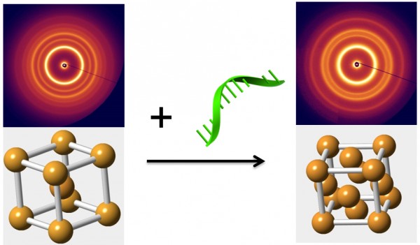
Using their method, the team demonstrated that they could switch their original nanoparticle array, the “mother” phase, into multiple different daughter phases with precision control.

Introducing “reprogramming” of DNA strands in an already assembled nanoparticle array triggers a transition from a “mother phase,” where particles occupy the corners and center of a cube (left), to a more compact “daughter phase” (right). The change represented in the schematic diagrams is revealed by the associated small-angle x-ray scattering patterns. Such phase-changes could potentially be used to switch a material’s properties on demand. (credit: Brookhaven National Laboratory)

DNA-based matter reprogramming

This is quite different from phase changes driven by external physical conditions such as pressure or temperature, Gang said, which typically result in single phase shifts, or sometimes sequential ones. “In those cases, to go from phase A to phase C, you first have to shift from A to B and then B to C,” said Gang. “Our method allows us to pick which daughter phase we want and go right to that one because the daughter phase is completely determined by the type of DNA reprogramming strands we use.”

The scientists were able to observe the structural transformations to various daughter phases using a technique called in situ small-angle x-ray scattering at the National Synchrotron Light Source, a DOE Office of Science User Facility that operated at Brookhaven Lab from 1982 until last September (now replaced by NSLS-II, which produces x-ray beams 10,000 times brighter). The team also used computational modeling to calculate how different kinds of reprogramming strands would alter the interparticle interactions, and found their calculations agreed well with their experimental observations.

“The ability to dynamically switch the phase of an entire superlattice array will allow the creation of reprogrammable and switchable materials wherein multiple, different functions can be activated on demand,” said Gang. “Our experimental work and accompanying theoretical analysis confirm that reprogramming DNA-mediated interactions among nanoparticles is a viable way to achieve this goal.”

This research was done in collaboration with scientists from Columbia University’s School of Engineering and Applied Science and the Indian Institute of Technology Gandhinagar. The work was funded by the DOE Office of Science.


Abstract of Selective transformations between nanoparticle superlattices via the reprogramming of DNA-mediated interactions

The rapid development of self-assembly approaches has enabled the creation of materials with desired organization of nanoscale components. However, achieving dynamic control, wherein the system can be transformed on demand into multiple entirely different states, is typically absent in atomic and molecular systems and has remained elusive in designed nanoparticle systems. Here, we demonstrate with in situ small-angle X-ray scattering that, by using DNA strands as inputs, the structure of a three-dimensional lattice of DNA-coated nanoparticles can be switched from an initial ‘mother’ phase into one of multiple ‘daughter’ phases. The introduction of different types of reprogramming DNA strands modifies the DNA shells of the nanoparticles within the superlattice, thereby shifting interparticle interactions to drive the transformation into a particular daughter phase. Moreover, we mapped quantitatively with free-energy calculations the selective reprogramming of interactions onto the observed daughter phases.