Creating complex structures using DNA origami and nanoparticles

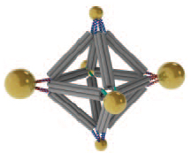
Cluster assembled from DNA-functionalized gold nanoparticles on vertices of a octahedral DNA origami frame (credit: Brookhaven National Laboratory))

Scientists at the U.S. Department of Energy’s (DOE) Brookhaven National Laboratory and collaborators have developed a method using DNA for designing new customized materials with complex structures for applications in energy, optics, and medicine.

They used ropelike configurations of DNA to form a rigid geometrical framework and then added dangling pieces of single-stranded DNA to glue nanoparticles in place.

The method, described in the journal Nature Nanotechnology, produced predictable geometric configurations that are somewhat analogous to molecules made of atoms, according to Brookhaven physicist Oleg Gang, who led the project at the Lab’s Center for Functional Nanomaterials (CFN).

“While atoms form molecules based on the nature of their chemical bonds, there has been no easy way to impose such a specific spatial binding scheme on nanoparticles, he said. “This is exactly the problem that our method addresses.

“We may be able to design materials that mimic nature’s machinery to harvest solar energy, or manipulate light for telecommunications applications, or design novel catalysts for speeding up a variety of chemical reactions,” Gang said.

As a demonstration, the researchers used an octahedral (eight-sided) scaffold (structure) with particles positioned in precise locations on the scaffold according to specific DNA coding. They also used the geometrical clusters as building blocks for larger arrays, including linear chains and two-dimensional planar sheets.

“Our work demonstrates the versatility of this approach and opens up numerous exciting opportunities for high-yield precision assembly of tailored 3D building blocks in which multiple nanoparticles of different structures and functions can be integrated,” said CFN scientist Ye Tian, one of the lead authors on the paper.

A new DNA “origami” kit
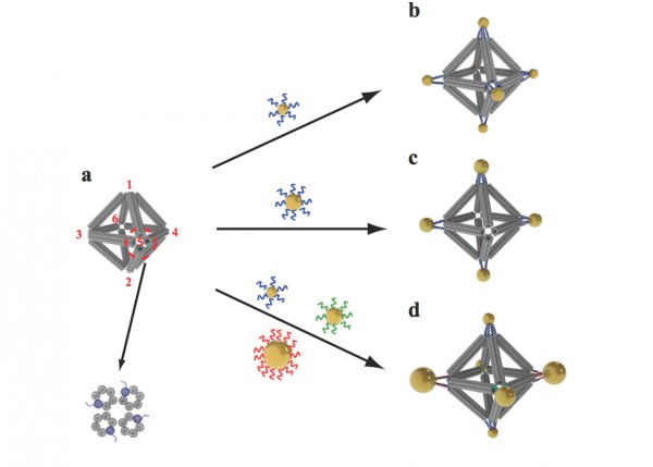
Scientists built octahedrons using ropelike structures made of bundles of DNA double-helix molecules to form the frames (a). Single strands of DNA attached at the vertices (numbered in red) can be used to attach nanoparticles coated with complementary strands. This approach can yield a variety of structures, including ones with the same type of particle at each vertex (b), arrangements with particles placed only on certain vertices (c), and structures with different particles placed strategically on different vertices (d). (credit: Brookhaven National Laboratory)

This nanoscale construction approach takes advantage of two key characteristics of the DNA molecule: the twisted-ladder double helix shape, and the natural tendency of strands with complementary bases (the A, T, G, and C letters of the genetic code) to pair up in a precise way.

Here’s how the scientists built a complex structure with this “DNA origami” kit:

1. They created bundles of six double-helix DNA molecules.

2. They put four of these bundles together to make a stable, somewhat rigid building material — similar to the way individual fibrous strands are woven together to make a very strong rope.

3. They used these ropelike girders to form the frame of three-dimensional octahedrons, “stapling” the linear DNA chains together with hundreds of short complementary DNA strands. (“We refer to these as DNA origami octahedrons,” Gang said.)

4. To make it possible to “glue” nanoparticles to the 3D frames, the scientists engineered each of the original six-helix bundles to have one helix with an extra single-stranded piece of DNA sticking out from both ends.

5. When assembled into the 3D octahedrons, each vertex of the frame had a few of these “sticky end” tethers available for binding with objects coated with complementary DNA strands.

“When nanoparticles coated with single strand tethers are mixed with the DNA origami octahedrons, the ‘free’ pieces of DNA find one another so the bases can pair up according to the rules of the DNA complementarity code. Thus the specifically DNA-encoded particles can find their correspondingly designed place on the octahedron vertices,” Gang explained.

A combination cryo-electron microscopy image of an octahedral frame with one gold nanoparticle bound to each of the six vertices, shown from three different angles. (Credit: Brookhaven National Laboratory)

The scientists can also change what binds to each vertex by changing the DNA sequences encoded on the tethers. In one experiment, they encoded the same sequence on all the octahedron’s tethers, and attached strands with a complementary sequence to gold nanoparticles. The result: One gold nanoparticle attached to each of octahedron’s six vertices.

In additional experiments,the scientists changed the sequence of some vertices and used complementary strands on different kinds of particles, illustrating that they could direct the assembly and arrangement of the particles in a very precise way.
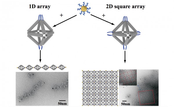
By strategically placing tethers on particular vertices, the scientists used the octahedrons to link nanoparticles into one-dimensional chainlike arrays (left) and two-dimensional square sheets (right). (Credit: Brookhaven National Laboratory)

In one case, they made two different arrangements of the same three pairs of particles of different sizes, producing products with different optical properties. They were even able to use DNA tethers on selected vertices to link octahedrons end-to-end, forming chains, and in 2D arrays, forming sheets.

Visualizing the structures
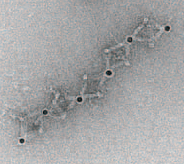
TEM image of part of the 1D array (credit: Brookhaven National Lab)

Confirming the particle arrangements and structures was a major challenge because the nanoparticles and the DNA molecules making up the frames have very different densities. Certain microscopy techniques would reveal only the particles, while others would distort the 3D structures.

To see both the particles and origami frames, the scientists used cryo-electron microscopy (cryo-EM), led by Brookhaven Lab and Stony Brook University biologist Huilin Li, an expert in this technique, and Tong Wang, the paper’s other lead co-author, who works in Brookhaven’s Biosciences department with Li.

They had to subtract information from the images to “see” the different density components separately, then combine the information using single particle 3D reconstruction and tomography to produce the final images.

This research was supported by the DOE Office of Science.


Abstract of Prescribed nanoparticle cluster architectures and low-dimensional arrays built using octahedral DNA origami frames

Three-dimensional mesoscale clusters that are formed from nanoparticles spatially arranged in pre-determined positions
can be thought of as mesoscale analogues of molecules. These nanoparticle architectures could offer tailored properties
due to collective effects, but developing a general platform for fabricating such clusters is a significant challenge. Here, we
report a strategy for assembling three-dimensional nanoparticle clusters that uses a molecular frame designed with
encoded vertices for particle placement. The frame is a DNA origami octahedron and can be used to fabricate clusters
with various symmetries and particle compositions. Cryo-electron microscopy is used to uncover the structure of the DNA
frame and to reveal that the nanoparticles are spatially coordinated in the prescribed manner. We show that the DNA
frame and one set of nanoparticles can be used to create nanoclusters with different chiroptical activities. We also show
that the octahedra can serve as programmable interparticle linkers, allowing one- and two-dimensional arrays to be
assembled with designed particle arrangements.

One step closer to a single-molecule device

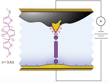
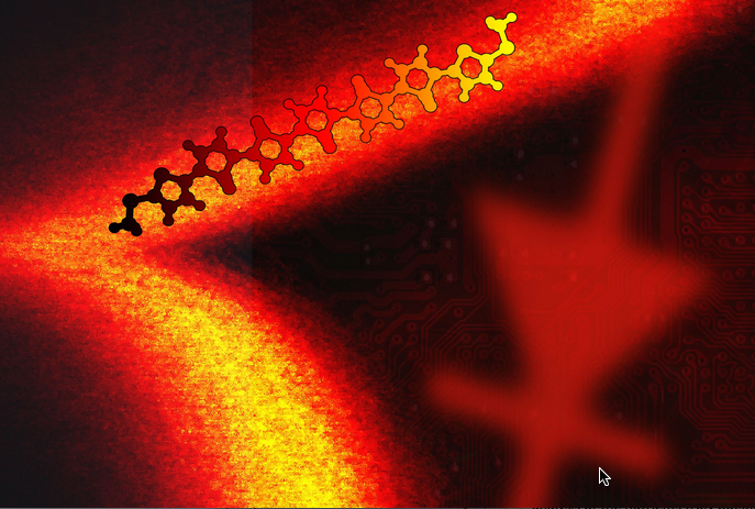
Molecular diode artist’s impression (credit: Columbia Engineering)

Columbia Engineering researchers have created the first single-molecule diode — the ultimate in miniaturization for electronic devices — with potential for real-world applications in electronic systems.

The diode that has a high (>250) rectification and a high “on” current (~ 0.1 microamps), says Latha Venkataraman, associate professor of applied physics. “Constructing a device where the active elements are only a single molecule … which has been the ‘holy grail’ of molecular electronics, represents the ultimate in functional miniaturization that can be achieved for an electronic device,” he said.

With electronic devices becoming smaller every day, the field of molecular electronics has become ever more critical in solving the problem of further miniaturization, and single molecules represent the limit of miniaturization. The idea of creating a single-molecule diode was suggested by Arieh Aviram and Mark Ratner who theorized in 1974 that a molecule could act as a rectifier, a one-way conductor of electric current.

The future of miniaturization

Single-molecule asymmetric molecular structure (alkyl side chains omitted for clarity) using a donor–bridge–acceptor architecture to mimic a semiconductor p–n junction (credit: Brian Capozzi et al./Nature Nanotechnology)

Researchers have since been exploring the charge-transport properties of molecules. They have shown that single-molecules attached to metal electrodes (single-molecule junctions) can be made to act as a variety of circuit elements, including resistors, switches, transistors, and, indeed, diodes.

They have learned that it is possible to see quantum mechanical effects, such as interference, manifest in the conductance properties of molecular junctions.

Since a diode acts as an electricity valve, its structure needs to be asymmetric so that electricity flowing in one direction experiences a different environment than electricity flowing in the other direction. To develop a single-molecule diode, researchers have simply designed molecules that have asymmetric structures.

“While such asymmetric molecules do indeed display some diode-like properties, they are not effective,” explains Brian Capozzi, a PhD student working with Venkataraman and lead author of the paper.

“A well-designed diode should only allow current to flow in one direction …  and it should allow a lot of current to flow in that direction. Asymmetric molecular designs have typically suffered from very low current flow in both ‘on’ and ‘off’ directions, and the ratio of current flow in the two has typically been low. Ideally, the ratio of ‘on’ current to ‘off’ current, the rectification ratio, should be very high.”

To overcome the issues associated with asymmetric molecular design, Venkataraman and her colleagues — Chemistry Assistant Professor Luis Campos’ group at Columbia and Jeffrey Neaton’s group at the Molecular Foundry at UC Berkeley — focused on developing an asymmetry in the environment around the molecular junction. They created an environmental asymmetry through a rather simple method: they surrounded the active molecule with an ionic solution and used gold metal electrodes of different sizes to contact the molecule.

Avoiding quantum-mechanical effects

Their results achieved rectification ratios as high as 250 — 50 times higher than earlier designs. The “on” current flow in their devices can be more than 0.1 microamps, which, Venkataraman notes, is a lot of current to be passing through a single-molecule. And, because this new technique is so easily implemented, it can be applied to all nanoscale devices of all types, including those that are made with graphene electrodes.

“It’s amazing to be able to design a molecular circuit, using concepts from chemistry and physics, and have it do something functional,” Venkataraman says. “The length scale is so small that quantum mechanical effects are absolutely a crucial aspect of the device. So it is truly a triumph to be able to create something that you will never be able to physically see and that behaves as intended.”

She and her team are now working on understanding the fundamental physics behind their discovery, and trying to increase the rectification ratios they observed, using new molecular systems.

The study, described in a paper published today (May 25) in Nature Nanotechnology, was funded by the National Science Foundation, the Department of Energy, and the Packard Foundation.

Combining light and sound to create nanoscale optical waveguides

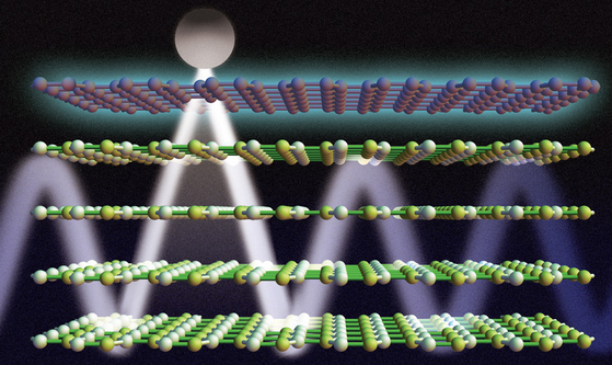
Researchers have shown that a DC voltage applied to layers of graphene and boron nitride can be used to control light emission from a nearby atom. Here, graphene is represented by a maroon-colored top layer; boron nitride is represented by yellow-green lattices below the graphene; and the atom is represented by a grey circle. A low concentration of DC voltage (in blue) allows the light to propagate inside the boron nitride, forming a tightly confined waveguide for optical signals. (credit: Anshuman Kumar Srivastava and Jose Luis Olivares/MIT)

In a new discovery that could lead to chips that combine optical and electronic components, researchers at MIT, IBM and two universities have found a way to combine light and sound with far lower losses than when such devices are made separately and then interconnected, they say.

Light’s interaction with graphene produces vibrating electron particles called plasmons, while light interacting with hexagonal boron nitride (hBN) produces phonons (sound “particles”). Fang and his colleagues found that when the materials are combined in a certain way, the plasmons and phonons can couple, producing a strong resonance.

The properties of the graphene allow precise control over light, while hBN provides very strong confinement and guidance of the light. Combining the two makes it possible to create new “metamaterials” that marry the advantages of both, the researchers say.

The work is co-authored by MIT associate professor of mechanical engineering Nicholas Fang and graduate student Anshuman Kumar, and their co-authors at IBM’s T.J. Watson Research Center, Hong Kong Polytechnic University, and the University of Minnesota.

According to Phaedon Avouris, a researcher at IBM and co-author of the paper, “The combination of these two materials provides a unique system that allows the manipulation of optical processes.”

The two materials are structurally similar — both composed of hexagonal arrays of atoms that form two-dimensional sheets — but they each interact with light quite differently. The researchers found that these interactions can be complementary, and can couple in ways that afford a great deal of control over the behavior of light.

The hybrid material blocks light when a particular voltage is applied to the graphene layer. When a different voltage is applied, a special kind of emission and propagation, called “hyperbolicity” occurs. This phenomenon has not been seen before in optical systems, Fang says.

Nanoscale optical waveguides

The result: an extremely thin sheet of material can interact strongly with light, allowing beams to be guided, funneled, and controlled by different voltages applied to the sheet.

The combined materials create a tuned system that can be adjusted to allow light only of certain specific wavelengths or directions to propagate, they say.

These properties should make it possible, Fang says, to create tiny optical waveguides, about 20 nanometers in size —- the same size range as the smallest features that can now be produced in microchips.

“Our work paves the way for using 2-D material heterostructures for engineering new optical properties on demand,” says co-author Tony Low, a researcher at IBM and the University of Minnesota.

Single-molecule optical resolution

Another potential application, Fang says, comes from the ability to switch a light beam on and off at the material’s surface; because the material naturally works at near-infrared wavelengths, this could enable new avenues for infrared spectroscopy, he says. “It could even enable single-molecule resolution,” Fang says, of biomolecules placed on the hybrid material’s surface.

Sheng Shen, an assistant professor of mechanical engineering at Carnegie Mellon University who was not involved in this research, says, “This work represents significant progress on understanding tunable interactions of light in graphene-hBN.” The work is “pretty critical” for providing the understanding needed to develop optoelectronic or photonic devices based on graphene and hBN, he says, and “could provide direct theoretical guidance on designing such types of devices. … I am personally very excited about this novel theoretical work.”

The research team also included Kin Hung Fung of Hong Kong Polytechnic University. The work was supported by the National Science Foundation and the Air Force Office of Scientific Research.


Abstract of Tunable Light–Matter Interaction and the Role of Hyperbolicity in Graphene–hBN System

Hexagonal boron nitride (hBN) is a natural hyperbolic material, which can also accommodate highly dispersive surface phonon-polariton modes. In this paper, we examine theoretically the mid-infrared optical properties of graphene–hBN heterostructures derived from their coupled plasmon–phonon modes. We find that the graphene plasmon couples differently with the phonons of the two Reststrahlen bands, owing to their different hyperbolicity. This also leads to distinctively different interaction between an external quantum emitter and the plasmon–phonon modes in the two bands, leading to substantial modification of its spectrum. The coupling to graphene plasmons allows for additional gate tunability in the Purcell factor and narrow dips in its emission spectra.

Printing low-cost, flexible radio-frequency antennas with graphene ink

These scanning electron microscope images show graphene ink after it was deposited and dried (a) and then compressed (b)k, which makes the graphene nanoflakes more dense, so it improves its electrical conductivity (credit: Xianjun Huang, et al./University of Manchester)

The first low-cost, flexible, environmentally friendly radio-frequency antenna using compressed graphene ink has been printed by researchers from the University of Manchester and BGT Materials Limited. Potential uses of the new process include radio-frequency identification (RFID) tags, wireless sensors, wearable electronics, and printing on materials like paper and plastic.

Commercial RFID tags are currently made from metals like silver (very expensive) or aluminum or copper (both prone to being oxidized).

Graphene conductive ink avoids those problems and can be used to print circuits and other electronic components, but the ink contains one or more polymeric, epoxy, siloxane, and resin binders. These are required to form a continuous (unbroken) conductive film. The problem is that these binders are insulators, so they reduce the conductivity of the connection. Also, applying the binder material requires annealing, a high-heat process (similar to how soldering with a resin binder works), which would destroy materials like paper or plastic.

Printing graphene ink on paper

So the researchers developed a new process:

1. Graphene flakes are mixed with a solvent and the ink it dried and deposited on the desired surface (paper, in the case of the experiment). (This is shown in step a in the illustration above.)

2. The flakes are compressed (step b above) with a roller (similar to using a roller to compress asphalt when making a road). That step increases the graphene’s conductivity by more than 50 times.

Graphene printed on paper (credit: Xianjun Huang et al./Applied Physics Letters)

The researchers tested their compressed graphene laminate by printing a graphene antenna onto a piece of paper. The material radiated radio-frequency power effectively, said Xianjun Huang, the first author of the paper and a PhD candidate in the Microwave and Communications Group in the School of Electrical and Electronic Engineering.

The researchers plan to further develop graphene-enabled RFID tags, as well as sensors and wearable electronics. They present their results in the journal Applied Physics Letters from AIP Publishing.


Abstract of Binder-free highly conductive graphene laminate for low cost printed radio frequency applications

In this paper we demonstrate realization of printable RFID antenna by low temperature processing of graphene ink. The required ultra-low resistance is achieved by rolling compression of binder-free graphene laminate. With compression, the conductivity of graphene laminate is increased by more than 50 times compared to that of as-deposited one. Graphene laminate with conductivity of 4.3×10⁴ S/m and sheet resistance of 3.8.

How to make continuous rolls of graphene for volume production

Diagram of the roll-to-roll process (a) shows the arrangement of copper spools at each end of the processing tube, and how a ribbon of thin copper substrate is wound around the central tube. Cross-section view of the same setup (b) shows the gap between two tubes, where the chemical vapor deposition process occurs. Photos of the system being tested show (c) the overall system, with an arrow indicating the direction the ribbon is moving; (d) a closeup of the copper ribbon inside the apparatus, showing the holes where chemical vapor is injected; and (e) an overhead view of the copper foil passing through the system. (credit: MIT and University of Michigan researchers)

A new graphene roll-to-roll continuous manufacturing process developed by MIT and University of Michigan researchers could finally take wonder-material graphene out of the lab and into practical commercial products.

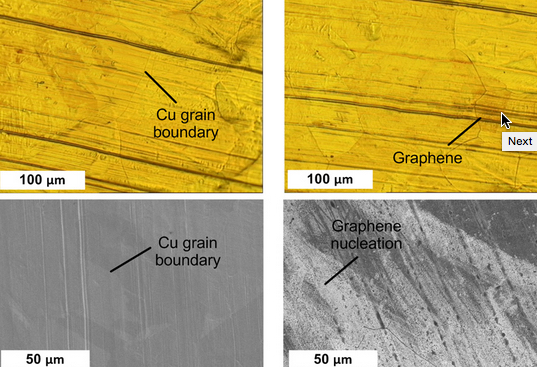
Copper substrate is shown in the process of being coated with graphene. At left, the process begins by treating the copper surface, and, at right, the graphene layer is beginning to form. Upper images are taken using visible light microscopy, and lower images using a scanning electron microscope. (credit: MIT and University of Michigan researchers)

The new process is an adaptation of a chemical vapor deposition method widely used to make graphene, using a small vacuum chamber into which a vapor containing carbon reacts on a horizontal substrate, such as a copper foil. The new system uses a similar vapor chemistry, but the chamber is in the form of two concentric tubes, one inside the other, and the substrate is a thin ribbon of copper that slides smoothly over the inner tube.

Gases flow into the tubes and are released through precisely placed holes, allowing for the substrate to be exposed to two mixtures of gases sequentially. The first region is called an annealing region, used to prepare the surface of the substrate; the second region is the growth zone, where the graphene is formed on the ribbon. The chamber is heated to approximately 1,000 degrees Celsius to perform the reaction.

The researchers have designed and built a lab-scale version of the system, and found that when the ribbon is moved through at a rate of 25 millimeters (1 inch) per minute, a very uniform, high-quality single layer of graphene is created. When rolled 20 times faster, it still produces a coating, but the graphene is of lower quality, with more defects.

A “big leap”

Graphene is a material with a host of potential applications, including use in solar panels that could be integrated into windows, and membranes to desalinate and purify water. But all these possible uses face the same big hurdle: the need for a scalable and cost-effective method for continuous manufacturing of graphene films.

For these practical uses, “You’re going to need to make acres of it, repeatedly and in a cost-effective manner,” says MIT mechanical engineering Associate Professor A. John Hart, senior author of the open-access Scientific Reports paper.

Making such quantities of graphene would represent a big leap from present approaches, where researchers struggle to produce small quantities of graphene — often laboriously pulling these sheets from a lump of graphite using adhesive tape, or producing a film the size of a postage stamp using a laboratory furnace.

The new method promises to enable continuous production, using a thin metal foil as a substrate, in an industrial process where the material would be deposited onto the foil as it smoothly moves from one spool to another. The resulting sheets would be limited in size only by the width of the rolls of foil and the size of the chamber where the deposition would take place.

Applications

Because a continuous process eliminates the need to stop and start to load and unload materials from a fixed vacuum chamber, as in today’s processing methods, it could lead to significant scale-up of production. That could finally unleash applications for graphene, which has unique electronic and optical properties and is one of the strongest materials known.

Some potential applications, such as filtration membranes, may require very high-quality graphene, but other applications, such as thin-film heaters may work well enough with lower-quality sheets, says Hart, who is the Mitsui Career Development Associate Professor in Contemporary Technology at MIT.

So far, the new system produces graphene that is “not quite [equal to] the best that can be done by batch processing,” Hart says — but “to our knowledge, it’s still at least as good” as what’s been produced by other continuous processes. Further work on details such as pretreatment of the substrate to remove unwanted surface defects could lead to improvements in the quality of the resulting graphene sheets, he says.

The team is studying these details, Hart adds, and learning about tradeoffs that can inform the selection of process conditions for specific applications, such as between higher production rate and graphene quality. Then, he says, “The next step is to understand how to push the limits, to get it 10 times faster or more.”

Hart says that while this study focuses on graphene, the machine could be adapted to continuously manufacture other two-dimensional materials, or even to growing arrays of carbon nanotubes, which his group is also studying.

“This is high-quality research that represents significant progress on the path to scalable production methods for large-area graphene,” says Charlie Johnson, a professor of physics and astronomy at the University of Pennsylvania who was not involved in this work. “I think that the concentric tube approach is very creative. It has the potential to lead to significantly lower production costs for graphene, if it can be scaled to larger copper-foil widths.”

The work was supported by the National Science Foundation and the Air Force Office of Scientific Research.

Nature inspires first artificial molecular pump

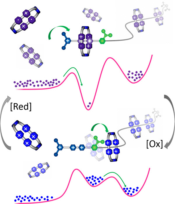
A blueprint for an artificial molecular pump that acts to organize rings in a high-energy state on a polymethylene chain. The flashing energy ratchet mechanism shows how redox chemistry can be used to prime the pump with rings (top) under reducing conditions and then have it pump the rings (bottom) under oxidative conditions into a high-energy state. Hypothetical distributions of the components of the pump on a simplified potential energy surface diagram are indicated by purple dots in the reduced state and blue dots in the oxidized state. A solid green arrow indicates a surmountable energy barrier. (credit: Chuyang Cheng et al./Nature Nanotechnology)

Northwestern University scientists have developed the first entirely artificial molecular pump, in which molecules pump other molecules. The pump might one day be used to power other molecular machines, such as artificial muscles.

The new machine mimics the pumping mechanism of proteins that move small molecules around living cells to metabolize and store energy from food. The artificial pump draws power from chemical reactions, driving molecules step-by-step from a low-energy state to a high-energy state — far away from equilibrium.

While nature has had billions of years to perfect its complex molecular machinery, modern science is now beginning to scratch the surface of what might be possible in tomorrow’s world.

Imitating how nature transfers energy

“Our molecular pump is radical chemistry — an ingenious way of transferring energy from molecule to molecule, the way nature does,” said Sir Fraser Stoddart, the senior author of the study. Stoddart is the Board of Trustees Professor of Chemistry in Northwestern’s Weinberg College of Arts and Sciences.

“All living organisms, including humans, must continuously transport and redistribute molecules around their cells, using vital carrier proteins,” he said. “We are trying to recreate the actions of these proteins using relatively simple small molecules we make in the laboratory.”

“In some respects, we are asking the molecules to behave in a way that they would not do normally,” Cheng said. “It is much like trying to push two magnets together. The ring-shaped molecules we work with repel one another under normal circumstances. The artificial pump is able to syphon off some of the energy that changes hands during a chemical reaction and uses it to push the rings together.”

The tiny molecular machine threads the rings around a nanoscopic chain — a sort of axle — and squeezes the rings together, with only a few nanometers separating them. At present, the artificial molecular pump is able to force only two rings together, but the researchers believe it won’t be long before they can extend its operation to tens of rings and store more energy.

Compared to nature’s system, the artificial pump is very simple, but it is a start, the researchers say. They have designed a novel system, using kinetic barriers, that allows molecules to flow “uphill” energetically.

Powering artificial muscles

“This is non-equilibrium chemistry, moving molecules far away from their minimum energy state, which is essential to life,” said Paul R. McGonigal, an author of the study. “Conducting non-equilibrium chemistry in this way, with simple artificial molecules, is one of the major challenges for science in the 21st century.”

Ultimately, they intend to use the energy stored in their pump to power artificial muscles and other molecular machines. The researchers also hope their design will inspire other chemists working in non-equilibrium chemistry.

“This is completely unlike the process of designing the machinery we are used to seeing in everyday life,” Stoddart said. “In a way, one must learn to see things from the molecules’ point of view, considering forces such as random thermal motion that one would never consider when building an agricultural water pump or any other mechanical device.”

The National Science Foundation supported the research, published May 18 in the journal Nature Nanotechnology.


Northwestern University | Artificial Molecular Pump Animation

Animation shows the steps of the pumping mechanism, which operates in response to redox cycling, with simplified illustrations of the corresponding energy profiles. The dumbbell and the ring repel each other initially, then reduction favors complexation both thermodynamically and kinetically. Oxidation restores the repulsion between the components and causes the ring to be trapped around the dumbbell during thermal relaxation. When another reduction step is performed, attraction of a second ring from the bulk solution is kinetically favored. After oxidation and thermal relaxation, the second ring falls into the same kinetic trap as the first, resulting in the mutually repulsive rings being held in close proximity to one another.


Abstract of An artificial molecular pump

Carrier proteins consume fuel in order to pump ions or molecules across cell membranes, creating concentration gradients. Their control over diffusion pathways, effected entirely through noncovalent bonding interactions, has inspired chemists to devise artificial systems that mimic their function. Here, we report a wholly artificial compound that acts on small molecules to create a gradient in their local concentration. It does so by using redox energy and precisely organized noncovalent bonding interactions to pump positively charged rings from solution and ensnare them around an oligomethylene chain, as part of a kinetically trapped entanglement. A redox-active viologen unit at the heart of a dumbbell-shaped molecular pump plays a dual role, first attracting and then repelling the rings during redox cycling, thereby enacting a flashing energy ratchet mechanism with a minimalistic design. Our artificial molecular pump performs work repetitively for two cycles of operation and drives rings away from equilibrium toward a higher local concentration.

How to print stronger, bigger, conductive 3-D graphene structures for tissue engineering

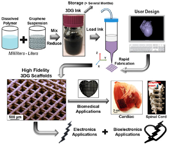
3D graphene inks are produced by simple combination and mixing an elastomer solution with graphene powder in a graded solvent, followed by volume reduction and thickening, a process that can be scaled up to many liters at once (credit: Adam E. Jakus et al./ACS Nano)

Northwestern University researchers have developed a way to print large, robust 3-D structures with graphene-based ink.

The new method could allow for using graphene-printed scaffolds for regenerative medicine and other medical and electronic  applications.

“People have tried to print graphene before,” said Ramille Shah, assistant professor of materials science and engineering at the McCormick School of Engineering and of surgery in the Feinberg School of Medicine.  “But it’s been a mostly polymer composite with graphene making up less than 20 percent of the volume.”

Adding higher volumes of graphene flakes to the mix in these ink systems typically results in printed structures too brittle and fragile to manipulate. At 60–70 percent graphene, the new ink preserves the material’s unique properties, including its electrical conductivity. And it’s flexible and robust enough to print robust macroscopic structures.

The secret: graphene nanoflakes are mixed with a biocompatible elastomer and fast-evaporating solvents.

“After the ink is extruded, one of the solvents in the system evaporates right away, causing the structure to solidify nearly instantly,” Shah explained. “The presence of the other solvents and the interaction with the specific polymer binder chosen also has a significant contribution to its resulting flexibility and properties. Because it holds its shape, we are able to build larger, well-defined objects.”

Could allow neurons to grow and communicate

Shah said her team populated one of the scaffolds with stem cells to surprising results. Not only did the cells survive; they divided, proliferated, and morphed into neuron-like cells.

The printed graphene structure is also flexible and strong enough to be easily sutured to existing tissues, so it could be used for biodegradable sensors and medical implants. Shah said the biocompatible elastomer and graphene’s electrical conductivity most likely contributed to the scaffold’s biological success.

“Cells conduct electricity inherently — especially neurons,” Shah said. “So if they’re on a substrate that can help conduct that signal, they’re able to communicate over wider distances.”

Supported by a Google Gift and a McCormick Research Catalyst Award, the research is described in the paper published in the April 2015 issue of ACS Nano.


Abstract of Three-Dimensional Printing of High-Content Graphene Scaffolds for Electronic and Biomedical Applications

The exceptional properties of graphene enable applications in electronics, optoelectronics, energy storage, and structural composites. Here we demonstrate a 3D printable graphene (3DG) composite consisting of majority graphene and minority polylactide-co-glycolide, a biocompatible elastomer, 3D-printed from a liquid ink. This ink can be utilized under ambient conditions via extrusion-based 3D printing to create graphene structures with features as small as 100 μm composed of as few as two layers (<300 μm thick object) or many hundreds of layers (>10 cm thick object). The resulting 3DG material is mechanically robust and flexible while retaining electrical conductivities greater than 800 S/m, an order of magnitude increase over previously reported 3D-printed carbon materials. In vitro experiments in simple growth medium, in the absence of neurogenic stimuli, reveal that 3DG supports human mesenchymal stem cell (hMSC) adhesion, viability, proliferation, and neurogenic differentiation with significant upregulation of glial and neuronal genes. This coincides with hMSCs adopting highly elongated morphologies with features similar to axons and presynaptic terminals. In vivo experiments indicate that 3DG has promising biocompatibility over the course of at least 30 days. Surgical tests using a human cadaver nerve model also illustrate that 3DG has exceptional handling characteristics and can be intraoperatively manipulated and applied to fine surgical procedures. With this unique set of properties, combined with ease of fabrication, 3DG could be applied toward the design and fabrication of a wide range of functional electronic, biological, and bioelectronic medical and nonmedical devices.

Wearables and electric vehicles may get boost from boron-infused graphene

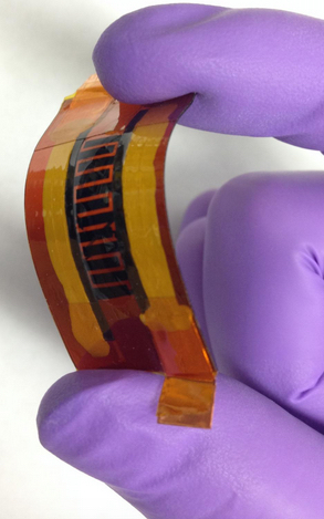
Rice University scientists made this supercapacitor with interlocked “fingers” using a laser and writing the pattern into a boron-infused sheet of polyimide. The device may be suitable for flexible, wearable electronics. (credit: Tour Group/Rice University)

Infusing the polymer in a laser-induced graphene supercapacitor (used to rapidly store and discharge electricity) with boric acid quadrupled the supercapacitor’s ability to store an electrical charge while greatly boosting its energy density (energy per unit volume), Rice University researchers have found.

The Rice lab of chemist James Tour uses commercial lasers to create thin, flexible supercapacitors by burning patterns into common polymers. The laser burns away everything but the carbon to a depth of 20 microns on the top layer, which becomes a foam-like matrix of interconnected graphene flakes.

Capacitors charge quickly and release their energy in a burst when needed, as in a camera flash. Supercapacitors add the high energy capacity of batteries and have potential for electric vehicles and other heavy-duty applications. But the potential to shrink them into a small, flexible, easily produced package could make them suitable for many more applications, including catalysts, field emission transistors, and components for solar cells and lithium-ion batteries, the researchers said.

In their earlier work, the team led by Rice graduate student Zhiwei Peng tried many polymers and discovered that a commercial polyimide was the best for the process. For the new work, the lab dissolved boric acid into polyamic acid and condensed it into a boron-infused polyimide sheet, which was then exposed to the laser.

Industrial-scale production

The two-step process produces microsupercapacitors with four times the ability to store an electrical charge and five to 10 times the energy density of the earlier, boron-free version.

The new devices proved highly stable over 12,000 charge-discharge cycles, retaining 90 percent of their capacitance. In stress tests, they handled 8,000 bending cycles with no loss of performance, the researchers reported.

Tour said the technique lends itself to industrial-scale, roll-to-roll production of microsupercapacitors. “What we’ve done shows that huge modulations and enhancements can be made by adding other elements and performing other chemistries within the polymer film prior to exposure to the laser,” he said.

Tour is the T.T. and W.F. Chao Chair in Chemistry as well as a professor of materials science and nanoengineering and of computer science and a member of Rice’s Richard E. Smalley Institute for Nanoscale Science and Technology.

The research is detailed in the journal ACS Nano.

The Air Force Office of Scientific Research and its Multidisciplinary University Research Initiative supported the research.


Abstract of Flexible Boron-Doped Laser Induced Graphene Microsupercapacitors

Heteroatom-doped graphene materials have been intensely studied as active electrodes in energy storage devices. Here, we demonstrate that boron-doped porous graphene can be prepared in ambient air using a facile laser induction process from boric acid containing polyimide sheets. At the same time, active electrodes can be patterned for flexible microsupercapacitors. As a result of boron doping, the highest areal capacitance of as-prepared devices reaches 16.5 mF/cm^2, three times higher than non-doped devices, with concomitant energy density increases of 5 to 10 times at various power densities. The superb cyclability and mechanical flexibility of the device is well-maintained, showing great potential for future microelectronics made from this boron-doped laser induced graphene material.

New graphene-like two-dimensional material could improve energy storage

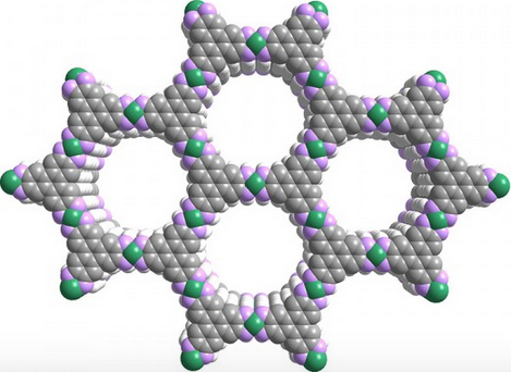
Porous, layered structure of highly conductive powder Ni3(HITP)2 (credit: Mircea Dinca, MIT)

MIT and Harvard University researchers have created a graphene-like electrically conductive. porous, layered material as possible new tool for storing energy and investigating the physics of unusual materials.

They synthesized the material using an organic molecule called HITP and nickel ions, forming a new compound: Ni3(HITP)2.

The new porous material is a crystalline, structurally tunable electrical conductor with a high surface area — features that are ideal for supercapacitors, which could extend the range of electric vehicles by capturing and storing the energy that would normally be wasted when brakes slow down a vehicle.

The new material is composed of stacks of unlimited numbers of two-dimensional sheets resembling graphite, with a room temperature electrical conductivity of ~40 S/cm (Siemens per centimeter). The conductivity of this material is comparable to that of bulk graphite and among the highest for any conducting Metal-organic frameworks (MOFs)* reported to date.

Also, the temperature-dependence of its conductivity linear at temperatures between 100 K (Kelvin) and 500 K, suggesting an unusual charge transport mechanism that has not been previously observed in any organic semiconductors, and thus remains to be investigated.

In bulk form, the material could be used for electrocatalysis applications (modifying the rate of chemical reactions) similar to how platinum works (but at lower cost). Upon exfoliation (peeling off of successive layers), the material is expected to behave similar to graphene, but with tunable bandgap and electromagnetic properties, suggesting new uses in electronic circuits and new exotic quantum properties in solid-state physics.

* MOFs are hybrid organic-inorganic materials that have traditionally been studied for gas storage or separation applications owing to their high surface area. Making good electrical conductors out of these normally insulating materials has been a long-standing challenge, as highly porous intrinsic conductors could be used for a range of applications, including energy storage.


Abstract of High Electrical Conductivity in Ni3(2,3,6,7,10,11-hexaiminotriphenylene)2, a Semiconducting Metal–Organic Graphene Analogue

Reaction of 2,3,6,7,10,11-hexaaminotriphenylene with Ni2+ in aqueous NH3 solution under aerobic conditions produces Ni3(HITP)2 (HITP = 2,3,6,7,10,11-hexaiminotriphenylene), a new two-dimensional metal–organic framework (MOF). The new material can be isolated as a highly conductive black powder or dark blue-violet films. Two-probe and van der Pauw electrical measurements reveal bulk (pellet) and surface (film) conductivity values of 2 and 40 S·cm–1, respectively, both records for MOFs and among the best for any coordination polymer.

Unraveling the mysteries of spider-web strength and damage-resistant design

Scientists at MIT have developed a systematic approach to research the structure of spider silk, blending computational modeling and mechanical analysis to 3D-print synthetic spider webs (credit: Zhao Qin et al./Nature Communications)

MIT scientists have developed a systematic approach to research the structure of spider “silk” (which ounce for ounce, is stronger than steel) and how spiders optimize their own webs. The researchers are  blending computational modeling and mechanical analysis to 3D-print synthetic spider webs, with the goal of fabricating and testing synthetic spider-web structures.

“This is the first methodical exploration of its kind,” says Professor Markus Buehler, head of MIT’s Department of Civil and Environmental Engineering (CEE), and the lead author of an open-access paper appearing in Nature Communications. “We are looking to expand our knowledge of the function of natural webs in a systematic and repeatable manner.”

The lessons learned through this approach may help harness spider silk’s strength for other uses, and ultimately inspire engineers to digitally design new structures and composites that are lighter, more reliable, and damage-resistant.

Reverse-engineering the spider’s sophisticated architecture

The study explores the relationship between spider web structure, loading points, and failure mechanisms. By adjusting the material distribution throughout an entire web, a spider is able to optimize the web’s strength for its anticipated prey.

The team, adopting an experimental setup, used metal structures to 3D-print synthetic webs, and directly integrate their data into models. “Ultimately we merged the physical with the computational in our experiments,” Buehler says.

According to Buehler, spider webs employ a limited amount of material to capture prey of different sizes, with materials only a few micrometers (millionths of a meter) in diameter.

The 3D-printed models, Lewis says, open the door to studying the effects of spider-web architecture on strength and damage tolerance — a feat that would have been impossible to achieve using only natural spider webs.

Buehler’s team used orb-weaver spider webs as the inspiration for their 3-D designs. In each of their samples, they controlled the diameter of the thread as a method of comparing homogeneous and heterogeneous thread thickness.

The work revealed that spider webs consisting of uniform thread diameters are better suited to bear force applied at a single point, such as the impact coming from flies hitting webs, while a nonuniform diameter can withstand more widespread pressure, such as from wind, rain, or gravity.

The team now plans to examine the dynamic aspects of webs through controlled impact and vibration experiments, changing the printed material’s properties in real time and opening the door to printing optimized, multifunctional structures.


Abstract of Structural optimization of 3D-printed synthetic spider webs for high strength

Spiders spin intricate webs that serve as sophisticated prey-trapping architectures that simultaneously exhibit high strength, elasticity and graceful failure. To determine how web mechanics are controlled by their topological design and material distribution, here we create spider-web mimics composed of elastomeric filaments. Specifically, computational modelling and microscale 3D printing are combined to investigate the mechanical response of elastomeric webs under multiple loading conditions. We find the existence of an asymptotic prey size that leads to a saturated web strength. We identify pathways to design elastomeric material structures with maximum strength, low density and adaptability. We show that the loading type dictates the optimal material distribution, that is, a homogeneous distribution is better for localized loading, while stronger radial threads with weaker spiral threads is better for distributed loading. Our observations reveal that the material distribution within spider webs is dictated by the loading condition, shedding light on their observed architectural variations.