How to condense water out of air using only sunlight for energy

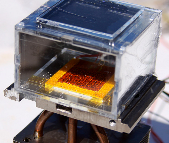
A water harvester designed and built at MIT condenses water from air. The harvester uses sunlight to heat metal-organic framework (MOF) material (inserted just below the glass plate on top), driving off the water vapor and condensing it (in the yellow and red condenser sitting at the bottom) for home use. (photo credit: Hyunho Kim/MIT)

MIT scientists have invented a water harvester that uses only sunlight to pull water out of the air under desert conditions, using a “metal-organic framework” (MOF) powdered material developed at the University of California, Berkeley (UC Berkeley).

Under conditions of 20–30 percent humidity (a level common in arid areas), the prototype device was able to pull 2.8 liters (3 quarts) of water from the air over a 12-hour period, using one kilogram (2.2 pounds) of MOF.

(Left) A schematic of metal-organic framework (MOF) material. The three large yellow, orange, and green balls are porous spaces for capturing and concentrating water molecules. (Right) As ambient air diffuses through the porous MOF, water molecules preferentially attach to the interior surfaces. Sunlight entering through a window heats up the MOF and drives the bound water toward the condenser, which is at the temperature of the outside air. The vapor condenses as liquid water and drips into a collector. (credit: UC Berkeley and MIT)

In 2014, a UC Berkeley team team led by chemist Omar Yaghi*, PhD, synthesized a porous MOF — a combination of zirconium metal and adipic acid** — that was able to bind water vapor. He suggested to Evelyn Wang, PhD, a mechanical engineer at MIT, that they join forces to turn the MOF into a water-collecting system.

Today (April 13, 2017), the system was announced in a paper published in the journal Science, with Yaghi and Wang as co-senior authors.***


“We wanted to demonstrate that if you are cut off somewhere in the desert, you could survive because of this device. A person needs about a Coke can of water per day. That is something one could collect in less than an hour with this system.” — Evelyn Wang


The new solar-powered harvester is a major breakthrough in the long-standing challenge of harvesting water from the air at low humidity, according to Yaghi. “There is no other way to do that right now, except by using extra energy. Your electric dehumidifier at home ‘produces’ very expensive water.”

Regions with desert climates (2011). Red: hot desert climates. Pink: cold desert climates. (credit: Koppen World Map/CC)

“We wanted to demonstrate that if you are cut off somewhere in the desert, you could survive because of this device,” Wang said. “A person needs about a Coke can of water per day. That is something one could collect in less than an hour with this system. … This work offers a new way to harvest water from air that does not require high relative humidity conditions and is much more energy efficient than other existing technologies.”

Running water and carbon-dioxide capture next

Yaghi and his team are currently working on improving their MOFs, while Wang continues to improve the harvesting system to produce more water.

The current MOF can absorb only 20 percent of its weight in water, but other MOF materials could possibly absorb 40 percent or more, and the material can be tweaked to be more effective at higher or lower humidity levels, Yaghi believes.
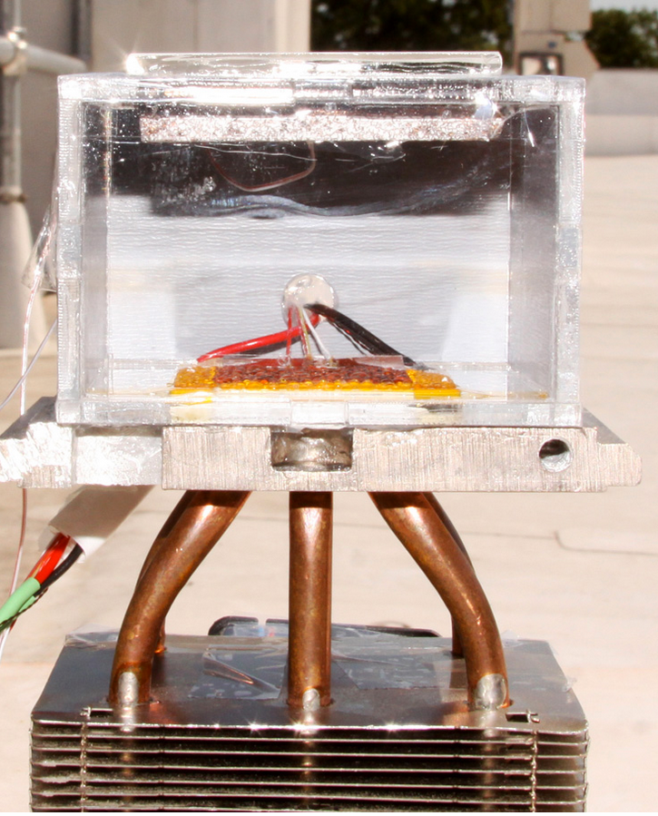
Rooftop tests at MIT confirmed that the water harvester works in real-world conditions. (photo credit: Hyunho Kim/MIT)

“It’s not just that we made a passive device that sits there collecting water; we have now laid both the experimental and theoretical foundations so that we can screen other MOFs, thousands of which could be made, to find even better materials,” he said. “There is a lot of potential for scaling up the amount of water that is being harvested. It is just a matter of further engineering now.”

“To have water running all the time, you could design a system that absorbs the humidity during the night and evolves it during the day,” Wang added. “Or design the solar collector to allow for this at a much faster rate, where more air is pushed in.”

Some MOFs being developed by Yaghi’s team could hold gases such as hydrogen or methane. The chemical company BASF is testing one of Yaghi’s MOFs in natural gas-fueled trucks; MOF-filled tanks hold three times the methane that can be pumped under pressure into an empty tank.

Other MOFs are able to capture carbon dioxide from flue gases, catalyze the reaction of adsorbed chemicals, or separate petrochemicals in processing plants.

* Yaghi holds the James and Neeltje Tretter chair in chemistry at UC Berkeley and is a faculty scientist at Lawrence Berkeley National Laboratory. He is also the founding director of the Berkeley Global Science Institute, and a co-director of the Kavli Energy NanoSciences Institute and the California Research Alliance by BASF. He invented metal-organic frameworks more than 20 years ago, combining metals like magnesium or aluminum with organic molecules in a tinker-toy arrangement to create rigid, porous structures ideal for storing gases and liquids. Since then, more than 20,000 different MOFs have been created by researchers worldwide.

** Metal-organic framework-801 [Zr6O4(OH)4(fumarate)6]

*** The work was supported in part by ARPA-E, a program of the U.S. Department of Energy. The work on MOFs in Yaghi’s laboratory is supported by BASF and the King Abdulaziz City for Science and Technology in Riyadh, Saudi Arabia.


UC Berkeley | Pulling drinkable water out of dry air

Omar Yaghi explains how to make a MOF and their tremendous ability to absorb gases and liquids, including water directly from low-humidity air. A MOF he synthesized was used by MIT engineers to construct a water harvester that sucks water from dry air and condenses it for drinking. Video by Roxanne Makasdjian and Stephen McNally, UC Berkeley. Harvester photos courtesy of MIT.


Abstract of Water harvesting from air with metal-organic frameworks powered by natural sunlight

Atmospheric water is a resource equivalent to ~10% of all fresh water in lakes on Earth. However, an efficient process for capturing and delivering water from air, especially at low humidity levels (down to 20%), has not been developed. We report the design and demonstration of a device based on porous metal-organic framework-801 [Zr6O4(OH)4(fumarate)6] that captures water from the atmosphere at ambient conditions using low-grade heat from natural sunlight below one sun (1 kW per square meter). This device is capable of harvesting 2.8 liters of water per kilogram of MOF daily at relative humidity levels as low as 20%, and requires no additional input of energy.

Graphene-oxide sieve turns seawater into drinking water

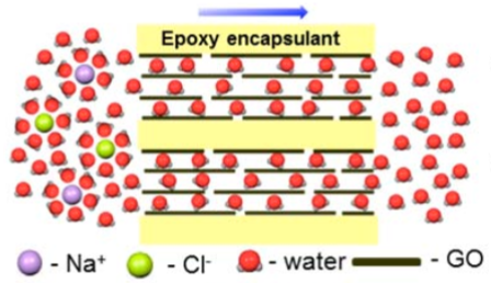
Schematic illustrating the direction of ion/water permeation along graphene planes (credit: J. Abraham et al./ Nature Nanotechnology)

British scientists have designed a way to use graphene-oxide (GO) membranes to filter common salts out of salty water and make the water safe to drink.

Graphene-oxide membranes developed at the National Graphene Institute had already demonstrated the potential of filtering out small nanoparticles, organic molecules, and even large salts. And previous research at The University of Manchester also found that if immersed in water, graphene-oxide membranes become slightly swollen and smaller salts flow through the membrane along with water, but larger ions or molecules are blocked.

The researchers have now found a strategy to avoid the swelling of the membrane when exposed to water by building smaller sieves. When the common salts are dissolved in water, they form a “shell” of water molecules around the salt molecules. This allows the tiny capillaries of the graphene-oxide membranes to block the salt from flowing along with the water. Water molecules are able to pass through the membrane barrier and flow  faster, which is ideal for application of these membranes for desalination.

“Realization of scalable membranes with uniform pore size down to atomic scale is a significant step forward and will open new possibilities for improving the efficiency of desalination technology,” said The University of Manchester Professor Rahul Nair.

The researchers also believe the atomic scale tunability of the pore size will make it possible in the future to fabricate membranes with on-demand filtration, capable of filtering out ions according to their sizes.

The research was published April 3, 2017 in the journal Nature Nanotechnology.

By 2025 the UN expects that 14% of the world’s population will encounter water scarcity. This technology has the potential to revolutionize water filtration across the world, in particular in countries which cannot afford large scale desalination plants, the researchers suggest.

The goal is to build membrane systems on smaller scales, making this technology accessible to countries that do not have the financial infrastructure to fund large plants without compromising the yield of fresh water produced.


The University of Manchester – The home of graphene | Graphene: Membranes and their practical applications


Abstract of Tunable sieving of ions using graphene oxide membranes

Graphene oxide membranes show exceptional molecular permeation properties, with promise for many applications. However, their use in ion sieving and desalination technologies is limited by a permeation cutoff of ∼9 Å, which is larger than the diameters of hydrated ions of common salts. The cutoff is determined by the interlayer spacing (d) of ∼13.5 Å, typical for graphene oxide laminates that swell in water. Achieving smaller d for the laminates immersed in water has proved to be a challenge. Here, we describe how to control d by physical confinement and achieve accurate and tunable ion sieving. Membranes with d from ∼9.8 Å to 6.4 Å are demonstrated, providing a sieve size smaller than the diameters of hydrated ions. In this regime, ion permeation is found to be thermally activated with energy barriers of ∼10–100 kJ mol–1 depending on d. Importantly, permeation rates decrease exponentially with decreasing sieve size but water transport is weakly affected (by a factor of <2). The latter is attributed to a low barrier for the entry of water molecules and large slip lengths inside graphene capillaries. Building on these findings, we demonstrate a simple scalable method to obtain graphene-based membranes with limited swelling, which exhibit 97% rejection for NaCl.

Neural probes for the spinal cord

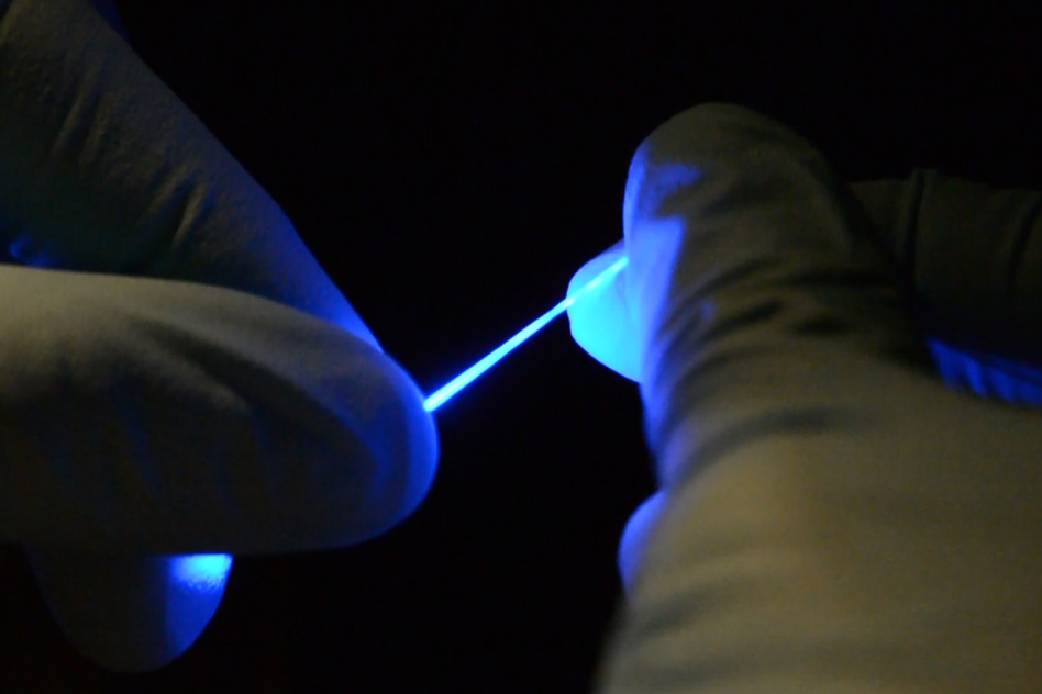
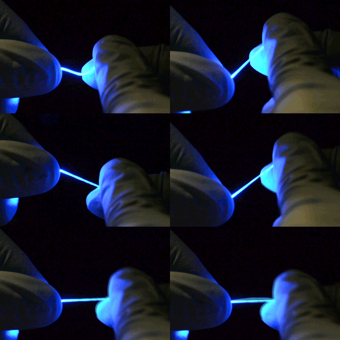
Researchers have developed a rubber-like fiber, shown here, that can flex and stretch while simultaneously delivering both optical impulses for optoelectronic stimulation,and electrical connections for stimulation and monitoring. (credit: Chi (Alice) Lu and Seongjun Park)

A research team led by MIT scientists has developed rubbery fibers for neural probes that can flex and stretch and be implanted into the mouse spinal cord.

The goal is to study spinal cord neurons and ultimately develop treatments to alleviate spinal cord injuries in humans. That requires matching the stretchiness, softness, and flexibility of the spinal cord. In addition, the fibers have to deliver optical impulses (for optoelectronic stimulation of neurons with blue or yellow laser light) and have electrical connections (for electrical stimulation and monitoring of neurons).

Implantable fibers have allowed brain researchers to stimulate specific targets in the brain and monitor electrical responses. But similar studies in the nerves of the spinal cord have been more difficult to carry out. That’s because the spine flexes and stretches as the body moves, and the relatively stiff, brittle fibers used today could damage the delicate spinal cord tissue.

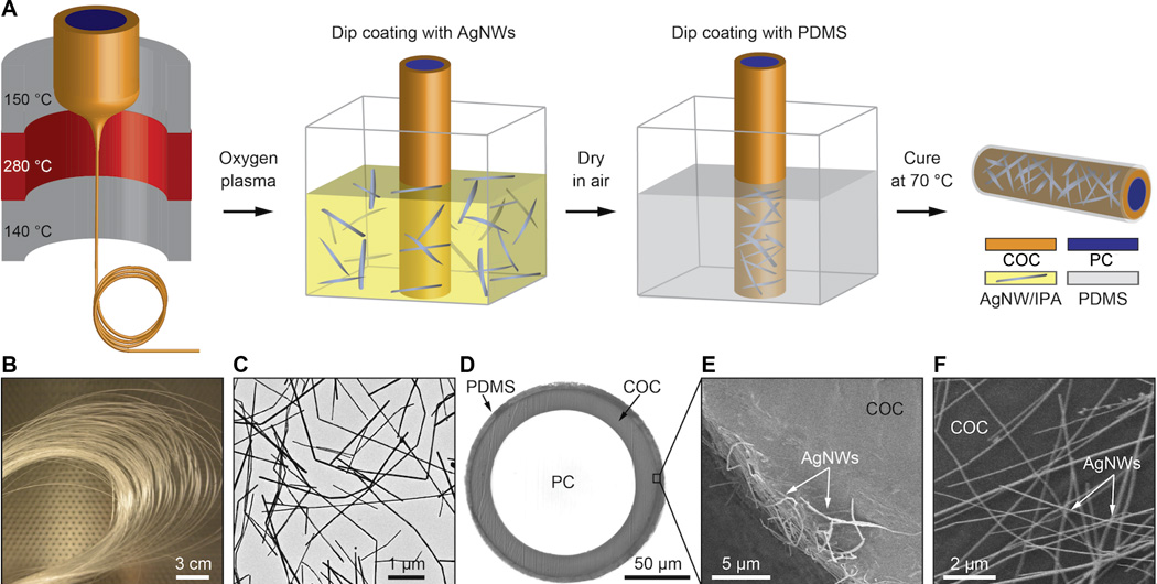
The scientists used a newly developed elastomer (a tough elastic polymer material that can flow and be stretched) that is transparent (like a fiber optic cable) for transmitting optical signals, and formed an external mesh coating of silver nanowires as a conductive layer for electrical signals. Think of it as tough, transparent, silver spaghetti.

Fabrication of flexible neural probes. (A) Thermal (heat) drawing produced a flexible optical fiber that also served as a structural core for the probe. (B) Spool of a fiber transparent polycarbonate (PC) core and cyclic olefin copolymer (COC) cladding, which enabled the fiber to be drawn into a fiber and was dissolved away after the drawing process. (C) Transmission electron microscopy (TEM) image of silver nanowires (AgNW). (D) Cross-sectional image of the fiber probe with biocompatible polydimethylsiloxane (PDMS) coating. (E) Scanning electron microscopy image showing a portion of the ring silver nanowire electrode cross section. (F) Scanning electron microscopy image of the silver nanowire mesh on top of the fiber surface. (credit: Chi Lu et al./Science Advances)

The fibers are “so floppy, you could use them to do sutures and deliver light  at the same time,” says MIT Professor Polina Anikeeva. The fiber can stretch by at least 20 to 30 percent without affecting its properties, she says. “Eventually, we’d like to be able to use something like this to combat spinal cord injury. But first, we have to have biocompatibility and to be able to withstand the stresses in the spinal cord without causing any damage.”

Scientists doing research on spinal cord injuries or disease usually must use larger animals in their studies, because the larger nerve fibers can withstand the more rigid wires used for stimulus and recording. While mice are generally much easier to study and available in many genetically modified strains, there was previously no technology that allowed them to be used for this type of research.

The fibers are not only stretchable but also very flexible. (credit: Chi (Alice) Lu and Seongjun Park)

The team included researchers at the University of Washington and Oxford University. The research was supported by the National Science Foundation, the National Institute of Neurological Disorders and Stroke, the U.S. Army Research Laboratory, and the U.S. Army Research Office through the Institute for Soldier Nanotechnologies at MIT.


Abstract of Flexible and stretchable nanowire-coated fibers for optoelectronic probing of spinal cord circuits

Studies of neural pathways that contribute to loss and recovery of function following paralyzing spinal cord injury require devices for modulating and recording electrophysiological activity in specific neurons. These devices must be sufficiently flexible to match the low elastic modulus of neural tissue and to withstand repeated strains experienced by the spinal cord during normal movement. We report flexible, stretchable probes consisting of thermally drawn polymer fibers coated with micrometer-thick conductive meshes of silver nanowires. These hybrid probes maintain low optical transmission losses in the visible range and impedance suitable for extracellular recording under strains exceeding those occurring in mammalian spinal cords. Evaluation in freely moving mice confirms the ability of these probes to record endogenous electrophysiological activity in the spinal cord. Simultaneous stimulation and recording is demonstrated in transgenic mice expressing channelrhodopsin 2, where optical excitation evokes electromyographic activity and hindlimb movement correlated to local field potentials measured in the spinal cord.

Magnetically storing a bit on a single atom — the ultimate future data storage

Dysprosium atoms (green) on the surface of nanoparticles can be magnetized in one of two possible directions: “spin up” or “spin down.” (credit: ETH Zurich / Université de Rennes)

Imagine you could store a bit on a single atom or small molecule — the ultimate magnetic data-storage system. An international team of researchers led by chemists from ETH Zurich has taken a step toward that idea by depositing single magnetizable atoms onto a silica surface, with the atoms retaining their magnetism.

In theory, certain atoms can be magnetized in one of two possible directions: “spin up” or “spin down” (representing zero or one); information could then be stored and read based on the sequence of the molecules’ magnetic spin directions. But finding molecules that can store the magnetic information permanently is a challenge, and it’s even more difficult to arrange these molecules on a solid surface to build actual data storage devices.

Magnetizing atoms on nanoparticles

Strategy for immobilization of dysprosium atoms (blue, surrounded by molecular scaffold) on a silica nanoparticle surface, based on a grafting step (a) and a thermolytic (chemical decomposition caused by heat) step (b) (credit: Florian Allouche et al./ ACS Central Science)

Nonetheless, Christophe Copéret, a professor at the Laboratory of Inorganic Chemistry at ETH Zurich, and his team have developed a method using a dysprosium atom (dysprosium is a metal belonging to the rare-earth elements). The atom is surrounded by a molecular scaffold that serves as a vehicle. The scientists also developed a method for depositing such molecules on the surface of silica nanoparticles and fusing them by annealing (heating) at 400 degrees Celsius.

The scaffold molecular structure disintegrates in the process, yielding nanoparticles with dysprosium atoms well-dispersed at the surface. The scientists showed that these atoms can then be magnetized and that they maintain their magnetic information.

One advantage of their new method is its simplicity. Nanoparticles bonded with dysprosium can be made in any chemical laboratory. No cleanroom and complex equipment required. And the magnetizable nanoparticles can be stored at room temperature and re-utilized.

Their magnetization process currently only works at around minus 270 degrees Celsius (near absolute zero), and the magnetization can only be maintained for up to one and a half minutes. So the scientists are now looking for methods that will allow the magnetization to be stabilized at higher temperatures and for longer periods of time. They are also looking for ways to fuse atoms to a flat surface instead of to spherical nanoparticles.

Other preparation methods also involve direct deposition of individual atoms onto a surface, but the materials are only stable at very low temperatures, mainly due to the agglomeration of these individual atoms. Alternatively, molecules with ideal magnetic properties can be deposited onto a surface, but this immobilization often negatively affects the structure and the magnetic properties of the final object.

Scientists from the Universities of Lyon and Rennes, Collège de France in Paris, Paul Scherrer Institute in Switzerland, and Berkeley National Laboratory were involved in the research.


Abstract of Magnetic Memory from Site Isolated Dy(III) on Silica Materials

Achieving magnetic remanence at single isolated metal sites dispersed at the surface of a solid matrix has been envisioned as a key step toward information storage and processing in the smallest unit of matter. Here, we show that isolated Dy(III) sites distributed at the surface of silica nanoparticles, prepared with a simple and scalable two-step process, show magnetic remanence and display a hysteresis loop open at liquid 4He temperature, in contrast to the molecular precursor which does not display any magnetic memory. This singular behavior is achieved through the controlled grafting of a tailored Dy(III) siloxide complex on partially dehydroxylated silica nanoparticles followed by thermal annealing. This approach allows control of the density and the structure of isolated, “bare” Dy(III) sites bound to the silica surface. During the process, all organic fragments are removed, leaving the surface as the sole ligand, promoting magnetic remanence.

Graphene-based neural probe detects brain activity at high resolution and signal quality

16 flexible graphene transistors (inset) integrated into a flexible neural probe enable electrical signals from neurons to be measured at high resolution and signal quality. (credit: ICN2)

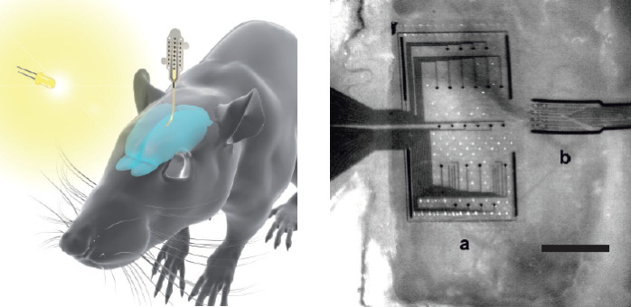
Researchers from the European Graphene Flagship* have developed a new microelectrode array neural probe based on graphene field-effect transistors (FETs) for recording brain activity at high resolution while maintaining excellent signal-to-noise ratio (quality).

The new neural probe could lay the foundation for a future generation of in vivo neural recording implants, for patients with epilepsy, for example, and for disorders that affect brain function and motor control, the researchers suggest. It could possibly play a role in Elon Musk’s just-announced Neuralink “neural lace” research project.

Measuring neural activity with high precision

(Left) Representation of the graphene implant placed on the surface of the rat’s brain. (Right) microscope image of a multielectrode array with conventional platinum electrodes (a) vs. the miniature graphene device next to it (b). Scale bar is 1.25 mm. (credit:  Benno M. Blaschke et al./ 2D Mater.)

Neural activity is measured by detecting the electric fields generated when neurons fire. These fields are highly localized, so ultra-small measuring devices that can be densely packed are required for accurate brain readings.

The new device has an microelectrode array of 16 graphene-based transistors arranged on a flexible substrate that can conform to the brain’s surface. Graphene provides biocompatibility, chemical stability, flexibility, and excellent electrical properties, which make it attractive for use in medical devices, especially for brain activity, the researchers suggest.**

(For a state-of-the-art example of microelectrode array use in the brain, see “Brain-computer interface advance allows paralyzed people to type almost as fast as some smartphone users.”)

Schematic of the head of a graphene implant showing a graphene transistor array and feed lines. (Inset): cross section of a graphene transistor with graphene between the source and drain contacts, which are covered by an insulating polyimide photoresist. (credit:  Benno M. Blaschke et al./ 2D Mater.)

In an experiment with rats, the researchers used the new devices to record brain activity during sleep and in response to visual light stimulation.

The graphene transistor probes showed good spatial discrimination (identifying specific locations) of the brain activity and outperformed state-of-the-art platinum electrode arrays, with higher signal amplification and a better signal-to-noise performance when scaled down to very small sizes.

That means the graphene transistor probes can be more densely packed and at higher resolution, features that are vital for precision mapping of brain activity. And since the probes have transistor amplifiers built in, they remove the need for the separate pre-amplification required with metal electrodes.

Neural probes are placed directly on the surface of the brain, so safety is important. The researchers determined that the flexible graphene-based probes are non-toxic, did not induce any significant inflammation, and are long-lasting.

“Graphene neural interfaces have shown already a great potential, but we have to improve on the yield and homogeneity of the device production in order to advance towards a real technology,” said Jose Antonio Garrido, who led the research at the Catalan Institute of Nanoscience and Nanotechnology in Spain.

“Once we have demonstrated the proof of concept in animal studies, the next goal will be to work towards the first human clinical trial with graphene devices during intraoperative mapping of the brain. This means addressing all regulatory issues associated to medical devices such as safety, biocompatibility, etc.”

The research was published in the journal 2D Materials.

* With a budget of €1 billion, the Graphene Flagship consortium consists of more than 150 academic and industrial research groups in 23 countries. Launched in 2013, the goal is to take graphene from the realm of academic laboratories into European society within 10 years. The research was a collaborative effort involving Flagship partners Technical University of Munich (TU Munich. Germany), Institut d’Investigacions Biomèdiques August Pi i Sunyer (IDIBAPS, Spain), Spanish National Research Council (CSIC, Spain), The Biomedical Research Networking Center in Bioengineering, Biomaterials and Nanomedicine (CIBER-BBN, Spain) and the Catalan Institute of Nanoscience and Nanotechnology (ICN2, Spain).

** “Using multielectrode arrays for high-density recordings presents important drawbacks. Since the electrode impedance and noise are inversely proportional to the electrode size, a trade-off between spatial resolution and signal-to-noise ratio has to be made. Further, the very small voltages of the recorded signals are highly susceptible to noise in the standard electrode configuration. [That requires preamplification, which means] the fabrication complexity is significantly increased and the additional electrical components required for the voltage-to-current conversion limit the integration density. … Metal-oxide-semiconductor field-effect transistors (MOSFETs) where the gate metal is replaced with an electrolyte and an electrode, referred to as “solution-gated field-effect transistors (SGFETs) or electrolyte-gated field-effect transistors, can be exposed directly to neurons and be used to record action potentials with high fidelity. … Although the potential of graphene-based SGFET technology has been suggested in in vitro studies, so far no in vivo confirmation has been demonstrated. Here we present the fabrication of flexible arrays of graphene SGFETs and demonstrate in vivo mapping of spontaneous slow waves, as well as visually evoked and pre-epileptic activity in the rat.” — Benno M. Blaschke et al./2D Mater.


Abstract of Mapping brain activity with flexible graphene micro-transistors

Establishing a reliable communication interface between the brain and electronic devices is of paramount importance for exploiting the full potential of neural prostheses. Current microelectrode technologies for recording electrical activity, however, evidence important shortcomings, e.g. challenging high density integration. Solution-gated field-effect transistors (SGFETs), on the other hand, could overcome these shortcomings if a suitable transistor material were available. Graphene is particularly attractive due to its biocompatibility, chemical stability, flexibility, low intrinsic electronic noise and high charge carrier mobilities. Here, we report on the use of an array of flexible graphene SGFETs for recording spontaneous slow waves, as well as visually evoked and also pre-epileptic activity in vivo in rats. The flexible array of graphene SGFETs allows mapping brain electrical activity with excellent signal-to-noise ratio (SNR), suggesting that this technology could lay the foundation for a future generation of in vivo recording implants.

A printable, sensor-laden ‘skin’ for robots (or an airplane)

Illustration of 3D-printed sensory composite (credit: Subramanian Sundaram)

MIT researchers have designed a radical new method of creating flexible, printable electronics that combine sensors and processing circuitry.

Covering a robot — or an airplane or a bridge, for example — with sensors will require a technology that is both flexible and cost-effective to manufacture in bulk. To demonstrate the feasibility of their new method, the researchers at MIT’s Computer Science and Artificial Intelligence Laboratory have designed and built a 3D-printed device that responds to mechanical stresses by changing the color of a spot on its surface.

Sensorimotor pathways

“In nature, networks of sensors and interconnects [such as the human nervous system] are called sensorimotor pathways,” says Subramanian Sundaram, an MIT graduate student in electrical engineering and computer science (EECS), who led the project. “We were trying to see whether we could replicate sensorimotor pathways inside a 3-D-printed object. So we considered the simplest organism we could find” — the golden tortoise beetle, or “goldbug,” an insect whose exterior usually appears golden but turns reddish orange if the insect is poked or prodded, that is, mechanically stressed.

The researchers present their new design in the latest issue of the journal Advanced Materials Technologies.

The key innovation was to 3D-print directly on the plastic substrate (support structure) instead of placing components on top. That greatly increases the range of devices that can be created; a printed substrate could consist of many materials, interlocked in intricate but regular patterns, which broadens the range of functional materials that printable electronics can use.*

Printed substrates also open the possibility of devices that, although printed as flat sheets, can fold themselves up into more complex, three-dimensional shapes. Printable robots that spontaneously self-assemble when heated, for instance (see “Self-assembling printable robotic components“), are a  topic of ongoing research at the CSAIL Distributed Robotics Laboratory, led by Daniela Rus, the Andrew and Erna Viterbi Professor of Electrical Engineering and Computer Science at MIT.

3D-printed sensory composite

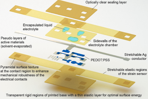
The sensory composite is grouped into 4 sets of functional layers: a base with spatially varying mechanical stiffness and surface energy, electrical materials, electrolyte, and capping layers. All these materials are 3D-printed. (credit: Subramanian Sundaram et al./ Advanced Materials Technologies)

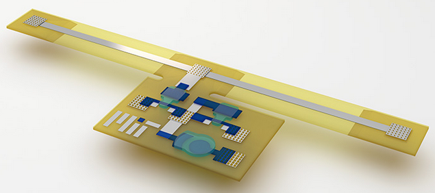
The MIT researchers’ new device is approximately T-shaped, but with a wide, squat base and an elongated crossbar. The crossbar is made from an elastic plastic, with a strip of silver running its length; in the researchers’ experiments, electrodes were connected to the crossbar’s ends. The base of the T is made from a more rigid plastic. It includes two printed transistors and what the researchers call a “pixel,” a circle of semiconducting polymer whose color changes when the crossbars stretch, modifying the electrical resistance of the silver strip.**

A transistor consists of semiconductor channel on top of which sits a “gate,” a metal wire that, when charged, generates an electric field that switches the semiconductor between its electrically conductive and nonconductive states. In a standard transistor, there’s an insulator between the gate and the semiconductor, to prevent the gate current from leaking into the semiconductor channel.

The transistors in the MIT researchers’ device instead separate the gate and the semiconductor with an electrolyte — a layer of water containing  potassium chloride mixed with glycerol. Charging the gate drives potassium ions into the semiconductor, changing its conductivity.***

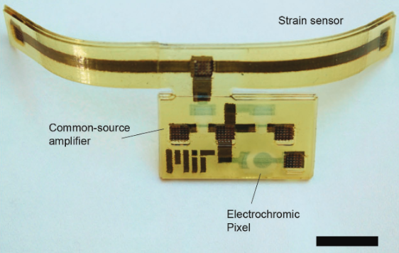
Photograph of the fully 3D-printed sensory composite shows a strain sensor (top) linked to an electrical amplifier that modulates the transparency of the electrochromic pixel (scale bar is 10mm). (credit: Subramanian Sundaram et al./ Advanced Materials Technologies)

“I am very impressed with both the concept and the realization of the system,” says Hagen Klauk, who leads the Organic Electronic Research Group at the Max Planck Institute for Solid State Research, in Stuttgart, Germany. “The approach of printing an entire optoelectronic system — including the substrate and all the components — by depositing all the materials, including solids and liquids, by 3-D printing is certainly novel, interesting, and useful, and the demonstration of the functional system confirms that the approach is also doable. By fabricating the substrate on the fly, the approach is particularly useful for improvised manufacturing environments where dedicated substrate materials may not be available.”

The work was supported by the DARPA SIMPLEX program through SPAWAR.

* To build the device, the researchers used the MultiFab, a custom 3-D printer developed MIT. The MultiFab already included two different “print heads,” one for emitting hot materials and one for cool, and an array of ultraviolet light-emitting diodes. Using ultraviolet radiation to “cure” fluids deposited by the print heads produces the device’s substrate.

** Sundaram added a copper-and-ceramic heater, which was necessary to deposit the semiconducting plastic: The plastic is suspended in a fluid that’s sprayed onto the device surface, and the heater evaporates the fluid, leaving behind a layer of plastic only 200 nanometers thick. The layer of saltwater lowers the device’s operational voltage, so that it can be powered with an ordinary 1.5-volt battery.

*** But it does render the device less durable. “I think we can probably get it to work stably for two months, maybe,” Sundaram says. “One option is to replace that liquid with something between a solid and a liquid, like a hydrogel, perhaps. But that’s something we would work on later. This is an initial demonstration.”


Abstract of 3D-Printed Autonomous Sensory Composites

A method for 3D-printing autonomous sensory composites requiring no external processing is presented. The composite operates at 1.5 V, locally performs active signal transduction with embedded electrical gain, and responds to stimuli, reversibly transducing mechanical strain into a transparency change. Digital assembly of spatially tailored solids and thin films, with encapsulated liquids, provides a route for realizing complex autonomous systems.

First nanoengineered retinal implant could help the blind regain functional vision

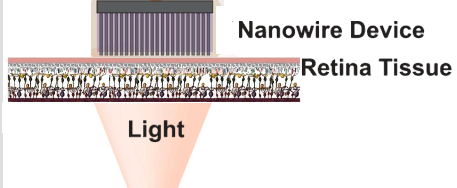
Activated by incident light, photosensitive silicon nanowires 1 micrometer in diameter stimulate residual undamaged retinal cells to induce visual sensations. (credit (image adapted): Sohmyung Ha et al./ J. Neural Eng)

A team of engineers at the University of California San Diego and La Jolla-based startup Nanovision Biosciences Inc. have developed the first nanoengineered retinal prosthesis — a step closer to restoring the ability of neurons in the retina to respond to light.

The technology could help tens of millions of people worldwide suffering from neurodegenerative diseases that affect eyesight, including macular degeneration, retinitis pigmentosa, and loss of vision due to diabetes.

Despite advances in the development of retinal prostheses over the past two decades, the performance of devices currently on the market to help the blind regain functional vision is still severely limited — well under the acuity threshold of 20/200 that defines legal blindness.

The new prosthesis relies on two new technologies: implanted arrays of photosensitive nanowires and a wireless power/data system.

Implanted arrays of silicon nanowires

The new prosthesis uses arrays of nanowires that simultaneously sense light and electrically stimulate the retina. The nanowires provide higher resolution than anything achieved by other devices — closer to the dense spacing of photoreceptors in the human retina, according to the researchers.*

Comparison of retina and electrode geometries between an existing retinal prosthesis and new nanoengineered prosthesis design. (left) Planar platinum electrodes (gray) of the FDA-approved Argus II retinal prosthesis (a 60-element array with 200 micrometer electrode diameter). (center) Retinal photoreceptor cells: rods (yellow) and cones (green). (right) Fabricated silicon nanowires (1 micrometer in diameter) at the same spatial magnification as photoreceptor cells. (credit: Science Photo Library and Sohmyung Ha et al./ J. Neural Eng.)

Existing retinal prostheses require a vision sensor (such as a camera) outside of the eye to capture a visual scene and then transform it into signals to sequentially stimulate retinal neurons (in a matrix). Instead, the silicon nanowires mimic the retina’s light-sensing cones and rods to directly stimulate retinal cells. The nanowires are bundled into a grid of electrodes, directly activated by light.

This direct, local translation of incident light into electrical stimulation makes for a much simpler — and scalable — architecture for a prosthesis, according to the researchers.

Wireless power and telemetry system

For the new device, power is delivered wirelessly, from outside the body to the implant, through an inductive powering telemetry system. Data to the nanowires is sent over the same wireless link at record speed and energy efficiency. The telemetry system is capable of transmitting both power and data over a single pair of inductive coils, one emitting from outside the body, and another on the receiving side in the eye.**

Three of the researchers have co-founded La Jolla-based Nanovision Biosciences, a partner in this study, to further develop and translate the technology into clinical use, with the goal of restoring functional vision in patients with severe retinal degeneration. Animal tests with the device are in progress, with clinical trials following.***

The research was described in a recent issue of the Journal of Neural Engineering. It was funded by Nanovision Biosciences, Qualcomm Inc., and the Institute of Engineering in Medicine and the Clinical and Translational Research Institute at UC San Diego.

* For visual acuity of 20/20,  an electrode pixel size of 5 μm (micrometers) is required; 20/200 visual acuity requires 50 μm. The minimum number of electrodes required for pattern recognition or reading text is estimated to be about 600. The new nanoengineered silicon nanowire electrodes are 1 μm in diameter, and for the experiment, 2500 silicon nanowires were used.

** The device is highly energy efficient because it minimizes energy losses in wireless power and data transmission and in the stimulation process, recycling electrostatic energy circulating within the inductive resonant tank, and between capacitance on the electrodes and the resonant tank. Up to 90 percent of the energy transmitted is actually delivered and used for stimulation, which means less RF wireless power emitting radiation in the transmission, and less heating of the surrounding tissue from dissipated power.

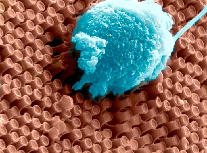
These are primary cortical neurons cultured on the surface of an array of optoelectronic nanowires. Here a neuron is pulling the nanowires, indicating the the cell is doing well on this material. (credit: UC San Diego)

*** For proof-of-concept, the researchers inserted the wirelessly powered nanowire array beneath a transgenic rat retina with rhodopsin P23H knock-in retinal degeneration. The degenerated retina interfaced in vitro with a microelectrode array for recording extracellular neural action potentials (electrical “spikes” from neural activity).


Abstract of Towards high-resolution retinal prostheses with direct optical addressing and inductive telemetry

Objective. Despite considerable advances in retinal prostheses over the last two decades, the resolution of restored vision has remained severely limited, well below the 20/200 acuity threshold of blindness. Towards drastic improvements in spatial resolution, we present a scalable architecture for retinal prostheses in which each stimulation electrode is directly activated by incident light and powered by a common voltage pulse transferred over a single wireless inductive link. Approach. The hybrid optical addressability and electronic powering scheme provides separate spatial and temporal control over stimulation, and further provides optoelectronic gain for substantially lower light intensity thresholds than other optically addressed retinal prostheses using passive microphotodiode arrays. The architecture permits the use of high-density electrode arrays with ultra-high photosensitive silicon nanowires, obviating the need for excessive wiring and high-throughput data telemetry. Instead, the single inductive link drives the entire array of electrodes through two wires and provides external control over waveform parameters for common voltage stimulation. Main results. A complete system comprising inductive telemetry link, stimulation pulse demodulator, charge-balancing series capacitor, and nanowire-based electrode device is integrated and validated ex vivo on rat retina tissue. Significance. Measurements demonstrate control over retinal neural activity both by light and electrical bias, validating the feasibility of the proposed architecture and its system components as an important first step towards a high-resolution optically addressed retinal prosthesis.

Resisting microcracks from metal fatigue

Researchers have developed a type of steel with three characteristics that help it resist microcracks that lead to fatigue failure: a layered nanostructure, a mixture of microstructural phases with different degrees of hardness, and a metastable composition. They compared samples of metal with just one or two of these key attributes (top left, top right, and bottom left) and with all three (bottom right). The metal alloy with all three attributes outperformed all the others in crack resistance. (credit: Courtesy of the researchers)

A team of researchers at MIT and in Japan and Germany has found a way to greatly reduce the effects of metal fatigue by incorporating a laminated nanostructure into the steel. The layered structuring gives the steel a kind of bone-like resilience, allowing it to deform without allowing the spread of microcracks that can lead to fatigue failure.

Metal fatigue can lead to abrupt and sometimes catastrophic failures in parts that undergo repeated loading, or stress. It’s a major cause of failure in structural components of everything from aircraft and spacecraft to bridges and power plants. As a result, such structures are typically built with wide safety margins that add to costs.

The findings are described in a paper in the journal Science by C. Cem Tasan, the Thomas B. King Career Development Professor of Metallurgy at MIT; Meimei Wang, a postdoc in his group; and six others at Kyushu University in Japan and the Max Planck Institute in Germany.

“Loads on structural components tend to be cyclic,” Tasan says. For example, an airplane goes through repeated pressurization changes during every flight, and components of many devices repeatedly expand and contract due to heating and cooling cycles. While such effects typically are far below the kinds of loads that would cause metals to change shape permanently or fail immediately, they can cause the formation of microcracks, which over repeated cycles of stress spread a bit further and wider, ultimately creating enough of a weak area that the whole piece can fracture suddenly.

Nature-inspired

Tasan and his team were inspired by the way nature addresses the same kind of problem, making bones lightweight but very resistant to crack propagation. A major factor in bone’s fracture resistance is its hierarchical mechanical structure, with different patterns of voids and connections at many different length scales, and a lattice-like internal structure that combines strength with light weight.

So the team investigated microstructures that would mimic this in a metal alloy, developing a kind of steel that has three key characteristics, which combine to limit the spread of cracks that do form:

  • A layered structure that tends to keep cracks from spreading beyond the layers where they start.
  • Microstructural phases with different degrees of hardness, which complement each other, so when a crack starts to form, “every time it wants to propagate further, it needs to follow an energy-intensive path,” and the result is a great reduction in such spreading.
  • A metastable composition — tiny areas within it are poised between different stable states, some more flexible than others, and their phase transitions can help absorb the energy of spreading cracks and even lead the cracks to close back up.

Next step, Tasan says, is to scale up the material to quantities that could be commercialized, and define which applications would benefit most.

The research was supported by the European Research Council and MIT’s Department of Materials Science and Engineering.


Abstract of Bone-like crack resistance in hierarchical metastable nanolaminate steels

Fatigue failures create enormous risks for all engineered structures, as well as for human lives, motivating large safety factors in design and, thus, inefficient use of resources. Inspired by the excellent fracture toughness of bone, we explored the fatigue resistance in metastability-assisted multiphase steels. We show here that when steel microstructures are hierarchical and laminated, similar to the substructure of bone, superior crack resistance can be realized. Our results reveal that tuning the interface structure, distribution, and phase stability to simultaneously activate multiple micromechanisms that resist crack propagation is key for the observed leap in mechanical response. The exceptional properties enabled by this strategy provide guidance for all fatigue-resistant alloy design efforts.

Engineers shrink atomic-force microscope to dime-sized device

A MEMS-based atomic force microscope developed by engineers at the University of Texas at Dallas that is about 1 square centimeter in size (top center), shown attached here to a small printed circuit board that contains circuitry, sensors and other miniaturized components that control the movement and other aspects of the device. (credit: University of Texas at Dallas)

University of Texas at Dallas researchers have created an atomic force microscope (AFM) on a chip, dramatically shrinking the size — and, hopefully, the price — of a microscope used to characterize material properties down to molecular dimensions.

“A standard atomic force microscope is a large, bulky instrument, with multiple control loops, electronics and amplifiers,” said Dr. Reza Moheimani, professor of mechanical engineering at UT Dallas.  “We have managed to miniaturize all of the electromechanical components down onto a single small chip.”

Moheimani and his colleagues describe their prototype device in this month’s issue of the IEEE Journal of Microelectromechanical Systems.

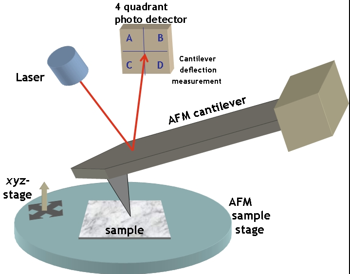
A conventional AFM consists of a tiny cantilever, or arm, that has a sharp tip attached to one end. As the apparatus scans back and forth across the surface of a sample, or the sample moves under it, the interactive forces between the sample and the tip cause the cantilever to move up and down as the tip follows the contours of the surface. Those movements are then translated into an image. (credit: CC/Opensource Handbook of Nanoscience and Nanotechnology)

An atomic force microscope (AFM) is a scientific tool that is used to create detailed three-dimensional images of the surfaces of materials, down to the nanometer scale — roughly on the scale of individual molecules.

“An AFM is a microscope that ‘sees’ a surface kind of the way a visually impaired person might, by touching. You can get a resolution that is well beyond what an optical microscope can achieve,” explained Moheimani, who holds the James Von Ehr Distinguished Chair in Science and Technology in the Erik Jonsson School of Engineering and Computer Science.

The MEMS version

The UT Dallas team created its prototype on-chip AFM using a microelectromechanical systems (MEMS) approach.

“A classic example of MEMS technology are the accelerometers and gyroscopes found in smartphones,” said Anthony Fowler, PhD, a research scientist in Moheimani’s Laboratory for Dynamics and Control of Nanosystems and one of the article’s co-authors. “These used to be big, expensive, mechanical devices, but using MEMS technology, accelerometers have shrunk down onto a single chip, which can be manufactured for just a few dollars apiece.”

The MEMS-based AFM is about 1 square centimeter in size, or a little smaller than a dime. It is attached to a small printed circuit board that contains circuitry, sensors, and other miniaturized components that control the movement and other aspects of the device.

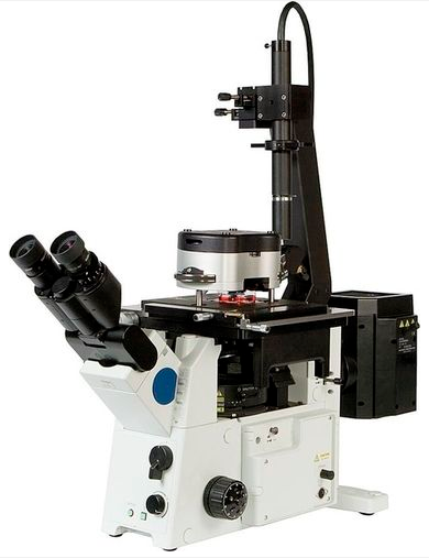
Conventional AFM (credit: Asylum Research, Inc.)

Because conventional AFMs require lasers and other large components to operate, their use can be limited. They’re also expensive. “An educational version can cost about $30,000 or $40,000, and a laboratory-level AFM can run $500,000 or more,” Moheimani said. “Our MEMS approach to AFM design has the potential to significantly reduce the complexity and cost of the instrument.

“One of the attractive aspects about MEMS is that you can mass-produce them, building hundreds or thousands of them in one shot, so the price of each chip would only be a few dollars. As a result, you might be able to offer the whole miniature AFM system for a few thousand dollars.”

Semiconductor-industry uses

A reduced size and price tag also could expand the AFMs’ utility beyond current scientific applications.

“For example, the semiconductor industry might benefit from these small devices, in particular companies that manufacture the silicon wafers from which computer chips are made,” Moheimani said. “With our technology, you might have an array of AFMs to characterize the wafer’s surface to find micro-faults before the product is shipped out.”

The lab prototype is a first-generation device, Moheimani said, and the group is already working on ways to improve and streamline the fabrication of the device.

Moheimani’s research has been funded by UT Dallas startup funds, the Von Ehr Distinguished Chair, and the Defense Advanced Research Projects Agency.


Abstract of On-Chip Dynamic Mode Atomic Force Microscopy: A Silicon-on-Insulator MEMS Approach

The atomic force microscope (AFM) is an invaluable scientific tool; however, its conventional implementation as a relatively costly macroscale system is a barrier to its more widespread use. A microelectromechanical systems (MEMS) approach to AFM design has the potential to significantly reduce the cost and complexity of the AFM, expanding its utility beyond current applications. This paper presents an on-chip AFM based on a silicon-on-insulator MEMS fabrication process. The device features integrated xy electrostatic actuators and electrothermal sensors as well as an AlN piezoelectric layer for out-of-plane actuation and integrated deflection sensing of a microcantilever. The three-degree-of-freedom design allows the probe scanner to obtain topographic tapping-mode AFM images with an imaging range of up to 8μm×8μm in closed loop. [2016-0211]