IBM-led international research team stores one bit of data on a single atom

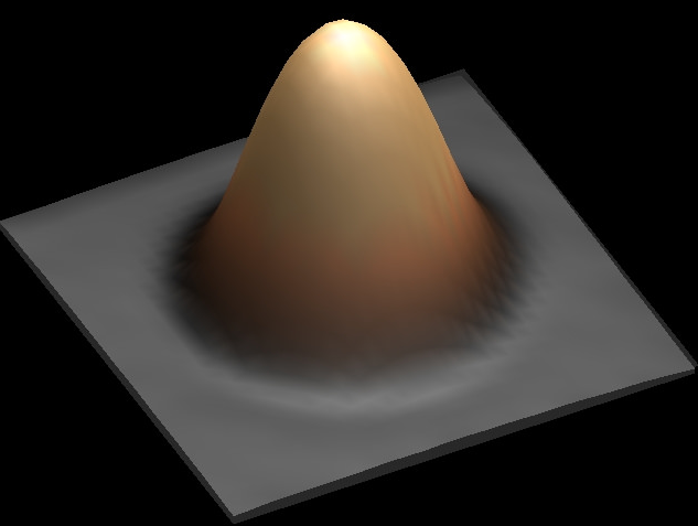
Scanning tunneling microscope image of a single atom of holmium, an element that researchers used as a magnet to store one bit of data. (credit: IBM Research — Almaden)

An international team led by IBM has created the world’s smallest magnet, using a single atom of rare-earth element holmium, and stored one bit of data on it over several hours.

The achievement represents the ultimate limit of the classical approach to high-density magnetic storage media, according to a paper published March 8 in the journal Nature.

Currently, hard disk drives use about 100,000 atoms to store a single bit. The ability to read and write one bit on one atom may lead to significantly smaller and denser storage devices in the future. (The researchers are currently working in an ultrahigh vacuum at 1.2 K (a temperature near absolute zero.)

Using a scanning tunneling microscope* (STM), the researchers also showed that a device using two magnetic atoms could be written and read independently, even when they were separated by just one nanometer.
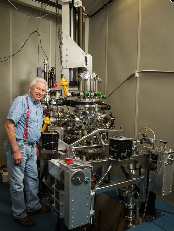
IBM microscope mechanic Bruce Melior at scanning tunneling microscope, used to view and manipulate atoms (credit: IBM Research — Almaden)

The researchers believe this tight spacing could eventually yield magnetic storage that is 1,000 times denser than today’s hard disk drives and solid state memory chips. So they could one day store 1,000 times more information in the same space. That means data centers, computers, and personal devices would be radically smaller and more powerful.
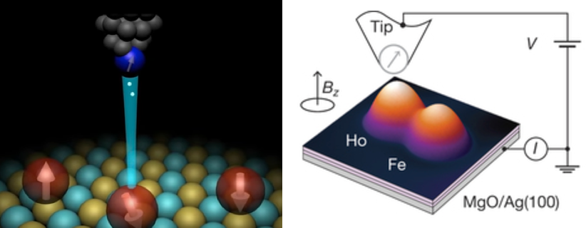
Single-atom write and read operations. (Left) To write the data onto the holmium atom, a pulse of electric current from the magnetized tip of a scanning tunneling microscope (STM) is used to flip the orientation of the atom’s field between a 0 or 1. The STM is also used to read it. (Right) A second read-out method used an iron atom as a magnetic sensor, which also allowed the team to read out multiple bits at the same time, making it more practical than an STM. (credit: IBM Research and Fabian D. Natterer et al./Nature)

Researchers at EPFL in Switzerland, University of Chinese Academy of Sciences in Hong Kong, University of Göttingen in Germany, Universität Zürich in Switzerland, Institute of Basic Science, Center for Quantum Nanoscience in South Korea, and Ewha Womans University in South Korea were also on the research team.

* The STM was developed in 1981, earning its inventors, Gerd Binnig and Heinrich Rohrer (at IBM Zürich), the Nobel Prize in Physics in 1986. IBM is planning future scanning tunneling microscope studies to investigate the potential of performing quantum information processing using individual magnetic atoms. Earlier this week, IBM announced it will be building the world’s first commercial quantum computers for business and science.


IBM Research | IBM Research Created the World’s Smallest Magnet — an Atom


Groundbreaking technology rewarms large-scale animal tissues preserved at low temperatures

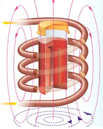
Inductive radio-frequency heating of magnetic nanoparticles embedded in tissue (red material in container) preserved at very low temperatures restored the tissue without damage (credit: Navid Manuchehrabadi et al./Science Translational Medicine)

A research team led by the University of Minnesota has discovered a way to rewarm large-scale animal heart valves and blood vessels preserved at very low (cryogenic) temperatures without damaging the tissue. The discovery could one day lead to saving millions of human lives by creating cryogenic tissue and organ banks of organs and tissues for transplantation.

The research was published March 1 in an open-access paper in Science Translational Medicine.

Long-term preservation methods like vitrification cool biological samples to an ice-free glassy state, using very low temperatures between -160 and -196 degrees Celsius, but tissues larger than 1 milliliter (0.03 fluid ounce) often suffer major damage during the rewarming process, making them unusable for tissues.

In the new research, the researchers were able to restore 50 milliliters (1.7 fluid ounces) of tissue with warming at more than 130°C/minute without damage.

Radiofrequency inductive heating of iron nanoparticles

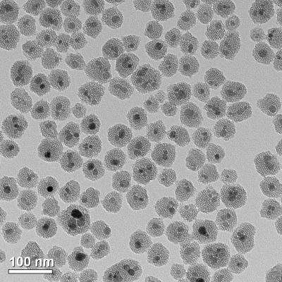
To achieve that, they developed a revolutionary new method using silica-coated iron-oxide nanoparticles dispersed throughout a cryoprotectant solution around the tissue. The nanoparticles act as tiny heaters around the tissue when they are activated using noninvasive radiofrequency inductive energy, rapidly and uniformly warming the tissue.

This transmission electron microscopy (TEM) image shows the iron oxide nanoparticles (coated in mesoporous silica) that are used in the tissue warming process. (credit: Haynes research group/University of Minnesota)

The results showed that none of the tissues displayed signs of harm — unlike control samples using vitrification and rewarmed slowly over ice or using convection warming. The researchers were also able to successfully wash away the iron oxide nanoparticles from the sample following the warming.

“This is the first time that anyone has been able to scale up to a larger biological system and demonstrate successful, fast, and uniform warming of hundreds of degrees Celsius per minute of preserved tissue without damaging the tissue,” said University of Minnesota mechanical engineering and biomedical engineering professor John Bischof, the senior author of the study.

Organs next

Bischof said there is a strong possibility they could scale up to even larger systems, like organs. The researchers plan to start with rodent organs (such as rat and rabbit) and then scale up to pig organs and then, hopefully, human organs. The technology might also be applied beyond cryogenics, including delivering lethal pulses of heat to cancer cells.

The researchers’ goal is to eliminate transplant waiting lists. Currently, hearts and lungs donated for transplantation must be discarded because these tissues cannot be kept on ice for longer than a matter of hours, according to the researchers.*

It will be interesting to see if the technology can one day be extended to cryonics.

The research was funded by the National Science Foundation (NSF), National Institutes of Health (NIH), U.S. Army Medical Research and Materiel Command, Minnesota Futures Grant from the University of Minnesota, and the University of Minnesota Carl and Janet Kuhrmeyer Chair in Mechanical Engineering. Researchers at Carnegie Mellon University, Clemson University and Tissue Testing Technologies LLC were also involved in the study.

* “A major limitation of transplantation is the ischemic injury that tissue and organs sustain during the time between recovery from the donor and implantation in the recipient. The maximum tolerable organ preservation for transplantation by hypothermic storage is typically 4 hours for heart and lungs; 8 to 12 hours for liver, intestine, and pancreas; and up to 36 hours for kidney transplants. In many cases, such limits actually prevent viable tissue or organs from reaching recipients. For instance, more than 60% of donor hearts and lungs are not used or transplanted partly because their maximum hypothermic preservation times have been exceeded. Further, if only half of these discarded organs were transplanted, then it has been estimated that wait lists for these organs could be extinguished within 2 to 3 years.” — Navid Manuchehrabadi et al./Science Translational Medicine


Abstract of Improved tissue cryopreservation using inductive heating of magnetic nanoparticles

Vitrification, a kinetic process of liquid solidification into glass, poses many potential benefits for tissue cryopreservation including indefinite storage, banking, and facilitation of tissue matching for transplantation. To date, however, successful rewarming of tissues vitrified in VS55, a cryoprotectant solution, can only be achieved by convective warming of small volumes on the order of 1 ml. Successful rewarming requires both uniform and fast rates to reduce thermal mechanical stress and cracks, and to prevent rewarming phase crystallization. We present a scalable nanowarming technology for 1- to 80-ml samples using radiofrequency-excited mesoporous silica–coated iron oxide nanoparticles in VS55. Advanced imaging including sweep imaging with Fourier transform and microcomputed tomography was used to verify loading and unloading of VS55 and nanoparticles and successful vitrification of porcine arteries. Nanowarming was then used to demonstrate uniform and rapid rewarming at >130°C/min in both physical (1 to 80 ml) and biological systems including human dermal fibroblast cells, porcine arteries and porcine aortic heart valve leaflet tissues (1 to 50 ml). Nanowarming yielded viability that matched control and/or exceeded gold standard convective warming in 1- to 50-ml systems, and improved viability compared to slow-warmed (crystallized) samples. Last, biomechanical testing displayed no significant biomechanical property changes in blood vessel length or elastic modulus after nanowarming compared to untreated fresh control porcine arteries. In aggregate, these results demonstrate new physical and biological evidence that nanowarming can improve the outcome of vitrified cryogenic storage of tissues in larger sample volumes.

Manipulating silicon atoms to create future ultra-fast, ultra-low-power chip technology

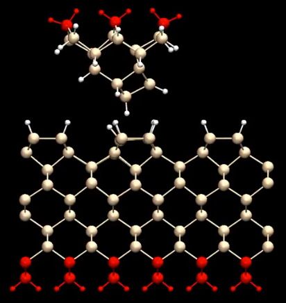
Model showing interactions between atomic-force microscope tip (top) and silicon surface (hydrogen: white; silicon: tan and red), using a new technique for coating the tip with hydrogen — part of a study to create future electronic circuits at the atomic level. (credit: Wolkow Lab)

Imagine a hybrid silicon-molecular computer that uses one thousand times less energy or a cell phone battery that lasts weeks at a time.

University of Alberta scientists, headed by University of Alberta physics professor Robert Wolkow, have taken a major step in that direction by visualizing and geometrically patterning silicon at the atomic level — using an innovative  atomic-force microscopy* (AFM) technique. The goal: chip technology that performs dramatically better than today’s CMOS architecture.

(Left) Ball-and-stick theoretical model of the pentacene molecule. (Right) AFM image of pentacene molecule showing the pattern of the bonds in the model. The five hexagonal carbon rings are resolved clearly and even the carbon-hydrogen bonds (white in the model) are imaged. Scale bar: 5 angstroms (0.5 nanometer) (credit: IBM Zurich)

Visualizing bonds in atoms at atomic resolution was first achieved by IBM Zurich scientists in 2009, when they imaged the pentacene molecule on copper. But imaging silicon is a problem: the sharp tip damages the fragile silicon molecules, the researchers note in an open-access paper published in the February 13, 2017 issue of Nature Communications.

To avoid damaging the silicon surface, the researchers created the first hydrogen-covered AFM tip, making it possible to manipulate silicon atoms. It was “a bit like Goldilocks,” PhD student and co-author Taleana Huff explained to KurzweilAI. “There is a sweet-spot region where you are probing the surface without interacting with it. Getting close enough to the surface with just the right parameters allows you to see these bonds materialize.

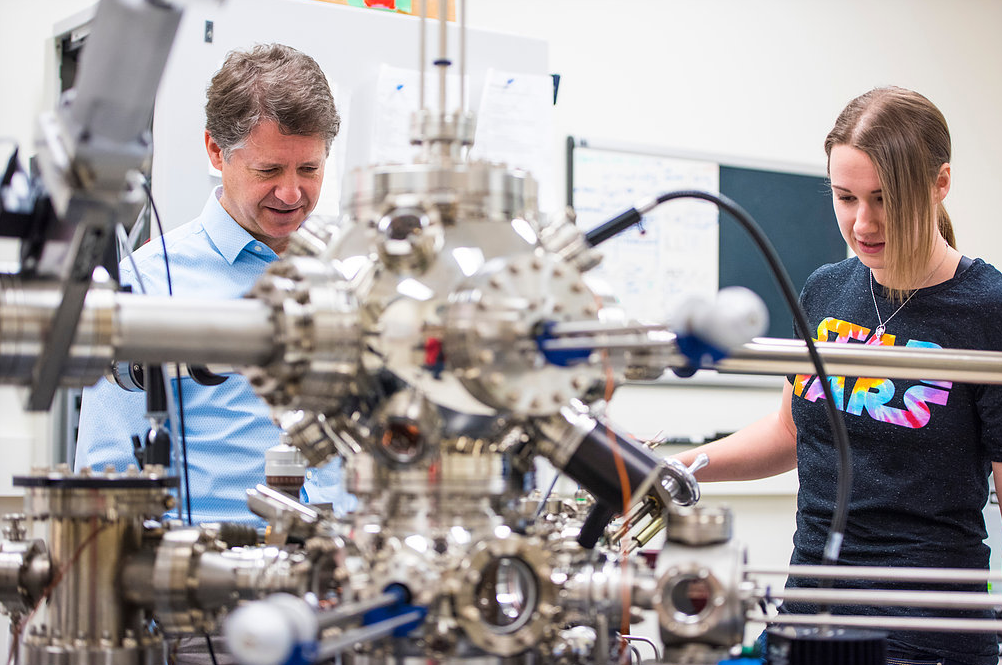
Bob Wolkow and Taleana Huff patterning and imaging electronic circuits at the atomic level (credit: Wolkow Lab)

“If you get too close though, you end up transferring atoms to the surface or, conversely, to the tip, ruining the experiment. A lot of tech and knowledge goes into getting all these settings just right, including a powerful new computational approach that analyzes and verifies the identity of the atoms and bonds.”

Hydrogen-terminated silicon for ultra-fast, ultra-low-power technology

“We see hydrogen-terminated silicon as the platform for a whole new paradigm of efficient and fast silicon-based electronics,” Huff said. “Now that we understand the surface intimately and have these powerful tools and the experience, the next step is to start using the AFM to look at computational elements made using quantum dots [nanoscale semiconductor particles], which we create by removing hydrogen atoms from the silicon surface. When we cleverly pattern them geometrically, these atomic silicon quantum dots can be used to make very fast and incredibly low-power computational patterns.”

The long-term goal is making ultra-fast and ultra-low-power silicon-based circuits that potentially consume one thousand times less power than what is currently on the market, according to the researchers, along with novel quantum applications.

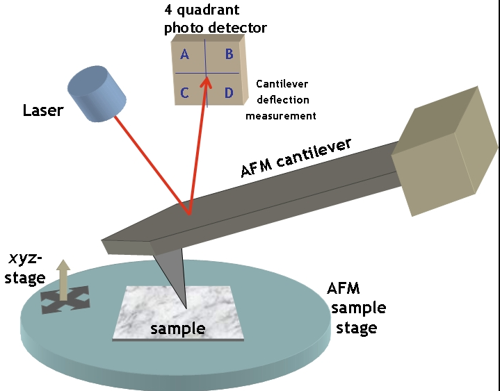
* Typical atomic force microscope (AFM) setup

To image a surface, an AFM sharp tip scans across the sample to detect irregularities in the surface, which cause deflection of the tip and the connected cantilever and generating a topological map of the sample surface. The deflection is measured by reflecting a laser beam off the backside of the cantilever. (credit: CC/Opensource Handbook of Nanoscience and Nanotechnology)


Wolkow Lab | An animation illustrating patterning and imagining electronic circuits at the atomic level. It shows the tip and surface atoms’ relaxation during calculations of a part of the image simulation at small tip-surface distance. The bending and rotation of bonds is visible, giving a sense of the interactions and atomic relaxations involved.


UAlbertaScience | Less is more for atomic-scale manufacturing

This animation represents an electrical current being switched on and off. Remarkably, the current is confined to a channel that is just one atom wide. Also, the switch is made of just one atom. When the atom in the center feels an electric field tugging at it, it loses its electron. Once that electron is lost, the many electrons in the body of the silicon (to the left) have a clear passage to flow through. When the electric field is removed, an electron gets trapped in the central atom, switching the current off. This represents the latest work out of Robert Wolkow’s lab at the University of Alberta.


Abstract of Indications of chemical bond contrast in AFM images of a hydrogen-terminated silicon surface

The origin of bond-resolved atomic force microscope images remains controversial. Moreover, most work to date has involved planar, conjugated hydrocarbon molecules on a metal substrate thereby limiting knowledge of the generality of findings made about the imaging mechanism. Here we report the study of a very different sample; a hydrogen-terminated silicon surface. A procedure to obtain a passivated hydrogen-functionalized tip is defined and evolution of atomic force microscopy images at different tip elevations are shown. At relatively large tip-sample distances, the topmost atoms appear as distinct protrusions. However, on decreasing the tip-sample distance, features consistent with the silicon covalent bonds of the surface emerge. Using a density functional tight-binding-based method to simulate atomic force microscopy images, we reproduce the experimental results. The role of the tip flexibility and the nature of bonds and false bond-like features are discussed.

Compact new microscope chemically identifies micrometer-sized particles

Multiple types of micrometer-sized particles are simultaneously illuminated by a far-infrared laser and a green laser beam. Absorption of the infrared laser energy by the particles increases their temperatures, causing them to expand and slightly altering their visible-light optical properties. These changes are unique to the material composition of each particle and can be measured by examining the modulation of scattered green light from each particle. (credit: Ryan Sullenberger, MIT Lincoln Laboratory)

MIT researchers have developed a radical design for a low-cost, miniaturized microscope that can chemically identify individual micrometer-sized particles. It could one day be used in airports or other high-security venues as a highly sensitive and low-cost way to rapidly screen people for microscopic amounts of potentially dangerous materials. It could also be used for scientific analysis of very small samples or for measuring the optical properties of materials.

Optical setup for PMMS measurement scheme. A tunable far-IR laser (QCL) or pump projects laser light (shown in this illustration as red, but actually invisible far-IR, or thermal energy) and a 532 nm laser (probe) projects green light onto the same location on a sample, which consists of microspheres deposited onto a ZnSe substrate in this experiment. A visible-light camera fitted with a 16× microscopic lens images the particles directly. The white LED is used to help locate the particles. (credit: R. M. Sullenberger et al./ Optics Letters)

In an open-access paper in the journal Optics Letters, from The Optical Society (OSA), the researchers demonstrated their new “photothermal modulation of Mie scattering” (PMMS) microscope by measuring infrared spectra of individual 3-micrometer spheres made of silica or acrylic. The new technique uses a simple optical setup consisting of compact components that will allow the instrument to be miniaturized into a portable device about the size of a shoebox.

The new microscope’s use of visible wavelengths for imaging gives it a spatial resolution of around 1 micrometer, compared to the roughly 10-micrometer resolution of traditional infrared spectroscopy methods. This increased resolution allows the new technique to distinguish and identify individual particles that are extremely small and close together.*

“If there are two very different particles in the field of view, we’re able to identify each of them,” said Stolyarov. “This would never be possible with a conventional infrared technique because the image would be indistinguishable.”

“The most important advantage of our new technique is its highly sensitive, yet remarkably simple design,” said Ryan Sullenberger, associate staff at MIT Lincoln Labs and first author of the paper. “It provides new opportunities for nondestructive chemical analysis while paving the way towards ultra-sensitive and more compact instrumentation.”

Probing spectral fingerprints

A typical far-IR spectrometer (credit: NYU)

Infrared spectroscopy is typically used to identify unknown materials because almost every material can be identified by its unique far-infrared absorption spectrum, or fingerprint. The new method detects this fingerprint without using actual far-infrared detectors, which add significant bulk to traditional instruments. That limits their use as portable devices — also because of their requirement for cooling.

The new technique works by illuminating particles with both an far-infrared laser and a green laser. The far-infrared laser deposits energy into the particles, causing them to heat up and expand. The green laser light is then scattered by these heated particles. A visible-wavelength camera is used to monitor this scattering, tracking physical changes of the individual particles through the microscope’s lens.

The instrument can be used to identify the material composition of individual particles by tuning the far-infrared laser to different wavelengths and collecting the visible scattered light at each wavelength. The slight heating of the particles doesn’t impart any permanent changes to the material, making the technique ideal for non-destructive analysis.

The ability to excite particles with infrared light and then look at their scattering with visible wavelengths — a process called photothermal modulation of Mie scattering — has been used since the 1980s. This new work uses more advanced optical components to create and detect the Mie scattering and is the first to use an imaging configuration to detect multiple species of particles.

“We’re actually imaging the area that we’re interrogating,” said Alexander Stolyarov, technical staff and a co-author of the paper. “This means we can simultaneously probe multiple particles on the surface at the same time.”

Compact, tunable infrared laser

The development of compact, tunable quantum-cascade infrared lasers was a key enabling technology for the new technique. The researchers combined a quantum-cascade laser with a very stable visible laser source and a commercially available scientific-grade camera.

“We are hoping to see an improvement in high-power wavelength-tunable quantum cascade lasers,” said Sullenberger. “A more powerful infrared laser enables us to interrogate larger areas in the same amount of time, allowing more particles to be probed simultaneously.”

The researchers plan to test their microscope on additional materials, including particles that are not spherical in shape. They also want to test their setup in more realistic environments that might contain interfering particles.

The work was supported by the U.S. Assistant Secretary of Defense for Research and Engineering under an Air Force contract.

* “By using a visible probe beam and camera for registering the particle absorption, we are able to spectroscopically identify individual particles that are spaced closer than the IR diffraction limit, which represents a significant improvement over conventional IR spectroscopic imaging techniques,” the authors note.


Abstract of Spatially-resolved individual particle spectroscopy using photothermal modulation of Mie scattering

We report a photothermal modulation of Mie scattering (PMMS) method that enables concurrent spatial and spectral discrimination of individual micron-sized particles. This approach provides a direct measurement of the “fingerprint” infrared absorption spectrum with the spatial resolution of visible light. Trace quantities (tens of picograms) of material were deposited onto an infrared-transparent substrate and simultaneously illuminated by a wavelength-tunable intensity-modulated quantum cascade pump laser and a continuous-wave 532 nm probe laser. Absorption of the pump laser by the particles results in direct modulation of the scatter field of the probe laser. The probe light scattered from the interrogated region is imaged onto a visible camera, enabling simultaneous probing of spatially-separated individual particles. By tuning the wavelength of the pump laser, the IR absorption spectrum is obtained. Using this approach, we measured the infrared absorption spectra of individual 3 μm PMMA and silica spheres. Experimental PMMS signal amplitudes agree with modeling using an extended version of the Mie scattering theory for particles on substrates, enabling the prediction of the PMMS signal magnitude based on the material and substrate properties.

Intricate microdevices that can be safely implanted

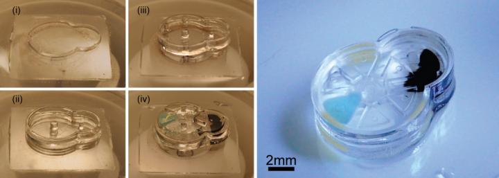
Fabrication and assembly of an iMEMS microdevice. Left: layer-by-layer fabrication of support structures and assembly of gear components. Right: the complete device after the layers have been sealed, with ferromagnetic iron material (black) to enable external magnetic control. (credit: SauYin Chin/Columbia Engineering)

Columbia Engineering researchers have invented a technique for manufacturing complex microdevices with three-dimensional, freely moving parts made from biomaterials that can safely be implanted in the body. Potential applications include a drug-delivery system to provide tailored drug doses for precision medicine, catheters, stents, cardiac pacemakers, and soft microbotics.

Most current implantable microdevices have static components rather than moving parts and, because they require batteries or other toxic electronics, they have limited biocompatibility.

The new technique stacks a soft biocompatible hydrogel material in layers, using a fast manufacturing method the researchers call “implantable microelectromechanical systems” (iMEMS).

iMEMS drug-delivery system. The payload delivery system was tested in a bone cancer mouse model, finding that the triggering of releases of doxorubicin from the device over 10 days showed high treatment efficacy and low toxicity, at 1/10th of the standard systemic chemotherapy dose. The device contains iron nanoparticle–doped components, which respond to external magnetic actuation. Actuation of the device triggers release of payloads from reservoirs. (credit: Sau Yin Chin et al./Science Robotics)

“Our iMEMS platform enables development of biocompatible implantable microdevices with a wide range of intricate moving components that can be wirelessly controlled on demand, and solves issues of device powering and biocompatibility,” says Biomedical Engineering Professor Sam Sia, senior author of an open-access paper published online January 4, 2017, in Science Robotics).

The researchers were able to trigger the iMEMS device to release payloads over days to weeks after implantation, with precise actuation by using magnetic forces to induce gear movements that, in turn, bend structural beams made of hydrogels with highly tunable properties. (Magnetic iron particles are commonly used and are FDA-approved for human use as contrast agents.)

Batteryless implantable medical devices or sensors

Sia’s iMEMS technique addresses several issues in building biocompatible microdevices, micromachines, and microrobots: how to power small robotic devices without using toxic batteries; how to make small, biocompatible, moveable components that are not silicon, which has limited biocompatibility; and how to communicate wirelessly once implanted (radio-frequency microelectronics require power, are relatively large, and are not biocompatible).

The researchers developed a “locking mechanism” for precise actuation and movement of freely moving parts, which can function as valves, manifolds, rotors, pumps, and drug delivery systems. They were able to tune the biomaterials within a wide range of mechanical and diffusive properties and to control them after implantation without a sustained power supply, such as a toxic battery.

“We can make small implantable devices, sensors, or robots that we can talk to wirelessly. Our iMEMS system could bring the field a step closer to developing soft miniaturized robots that can safely interact with humans and other living systems,” said Sia.

The team developed a drug delivery system and tested it on mice with bone cancer. The iMEMS system delivered chemotherapy adjacent to the cancer, and limited tumor growth while showing less toxicity than with chemotherapy administered throughout the body.

The study was supported by the National Science Foundation, NIH, and the Agency for Science, Technology and Research (Singapore).

* The team used light to polymerize sheets of gel and incorporated a stepper mechanization to control the z-axis and pattern the sheets layer by layer, giving them three-dimensionality. Controlling the z-axis enabled the researchers to create composite structures within one layer of the hydrogel while managing the thickness of each layer throughout the fabrication process. They were able to stack multiple layers that are precisely aligned and, because they could polymerize a layer at a time, one right after the other, the complex structure was built in under 30 minutes.

Hydrogels are difficult to work with, as they are soft and not compatible with traditional machining techniques,” says Sau Yin Chin, lead author of the study, who worked with Sia. “We have tuned the mechanical properties and carefully matched the stiffness of structures that come in contact with each other within the device. Gears that interlock have to be stiff in order to allow for force transmission and to withstand repeated actuation. Conversely, structures that form locking mechanisms have to be soft and flexible to allow for the gears to slip by them during actuation, while at the same time they have to be stiff enough to hold the gears in place when the device is not actuated. We also studied the diffusive properties of the hydrogels to ensure that the loaded drugs do not easily diffuse through the hydrogel layers.”


Abstract of Additive manufacturing of hydrogel-based materials for next-generation implantable medical devices

Implantable microdevices often have static components rather than moving parts and exhibit limited biocompatibility. This paper demonstrates a fast manufacturing method that can produce features in biocompatible materials down to tens of micrometers in scale, with intricate and composite patterns in each layer. By exploiting the unique mechanical properties of hydrogels, we developed a “locking mechanism” for precise actuation and movement of freely moving parts, which can provide functions such as valves, manifolds, rotors, pumps, and delivery of payloads. Hydrogel components could be tuned within a wide range of mechanical and diffusive properties and can be controlled after implantation without a sustained power supply. In a mouse model of osteosarcoma, triggering of release of doxorubicin from the device over 10 days showed high treatment efficacy and low toxicity, at 1/10 of the standard systemic chemotherapy dose. Overall, this platform, called implantable microelectromechanical systems (iMEMS), enables development of biocompatible implantable microdevices with a wide range of intricate moving components that can be wirelessly controlled on demand, in a manner that solves issues of device powering and biocompatibility.

Nanowire ‘inks’ enable low-cost paper- or plastic-based printable electronics

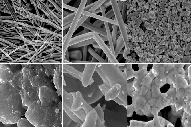
Duke University chemists have found that silver nanowire films like these conduct electricity well enough to form functioning circuits without applying high temperatures, enabling printable electronics on materials like paper or plastic. (credit: Ian Stewart and Benjamin Wiley)

By suspending tiny metal nanoparticles in liquids, Duke University scientists can use conductive ink-jet-printed conductive “inks” to print inexpensive, customizable RFID and other electronic circuit patterns on just about any surface — even on paper and plastics.

Printed electronics, which are already being used widely in devices such as the anti-theft radio frequency identification (RFID) tags you might find on the back of new DVDs, currently have one major drawback: for the circuits to work, they first have to be heated to 200° C (392°F) to melt all the nanoparticles together into a single conductive wire.

But Duke researchers have now found that electrons are conducted through films made of silver nanowires much more easily than with films made from other shapes (like nanospheres or microflakes). And the nanowire films can now function in printed circuits without the need to melt them first — heating at only 70° C (158°F) is required — and that means the circuits can be printed on cheaper plastics or paper.

“The nanowires [in their research] had a 4,000 times higher conductivity than the more commonly used silver nanoparticles that you would find in printed antennas for RFID tags,” said Benjamin Wiley, assistant professor of chemistry at Duke.

The technology could also be used to make lower-cost solar cells, printed displays, LEDs, touchscreens, amplifiers, batteries, and even some implantable bio-electronic devices. The results appeared online Dec. 16 in ACS Applied Materials and Interfaces.

The team is now experimenting with using aerosol jets to print silver nanowire inks in usable circuits. Wiley says they also want to explore whether silver-coated copper nanowires, which are significantly cheaper to produce than pure silver nanowires, will give the same effect.

This research was supported by funding from the National Science Foundation and a GAANN Fellowship through the Duke Chemistry Department.


Abstract of Effect of Morphology on the Electrical Resistivity of Silver Nanostructure Films

The relatively high temperatures (>200 °C) required to sinter silver nanoparticle inks have limited the development of printed electronic devices on low-cost, heat-sensitive paper and plastic substrates. This article explores the change in morphology and resistivity that occurs upon heating thick films of silver nanowires (of two different lengths; Ag NWs), nanoparticles (Ag NPs), and microflakes (Ag MFs) at temperatures between 70 and 400 °C. After heating at 70 °C, films of long Ag NWs exhibited a resistivity of 1.8 × 10⁻⁵ Ω cm, 4000 times more conductive than films made from Ag NPs. This result indicates the resistivity of thick films of silver nanostructures is dominated by the contact resistance between particles before sintering. After sintering at 300 °C, the resistivity of short Ag NWs, long Ag NWs, and Ag NPs converge to a value of (2–3) × 10–5 Ω cm, while films of Ag MFs remain ∼10× less conductive (4.06 × 10⁻⁴ Ω cm). Thus, films of long Ag NW films heated at 70 °C are more conductive than Ag NP films sintered at 300 °C. Adding 10 wt % nanowires to a film of nanoparticles results in a 400-fold improvement in resistivity.

A transparent, self-healing, highly stretchable conductive material

This illustration shows use of an ion-dipole interaction and self-healing material. (credit: University of Colorado, Boulder)

A team of scientists has developed a transparent, self-healing, highly stretchable conductive material that can be electrically activated to power artificial muscles or used to improve batteries, electronic devices, and robots.

The findings, published Dec. 23 in the journal Advanced Materials, combine the fields of self-healing materials and ionic conductors (a material that ions can flow through). Ionic conductors are a class of materials with key roles in energy storage, solar energy conversion, sensors, and electronic devices.

The material has potential applications in a wide range of fields. It could give robots the ability to self-heal after mechanical failure, extend the lifetime of lithium ion batteries used in electronics and electric cars, and improve biosensors used in the medical field and environmental monitoring, the scientists say.

Inspired by wound healing in nature, the idea for self-healing materials is to repair damage caused by wear, lower the cost of materials and devices, and extend their lifetime.

“Creating a material with all these properties has been a puzzle for years,” said Chao Wang*, a University of California, Riverside adjunct assistant professor of chemistry who is one of the authors of a paper published in December in Advanced Materials.

Another author of the paper, Christoph Keplinger, an assistant professor at the University of Colorado, Boulder, previously demonstrated that stretchable, transparent, ionic conductors can be used to power artificial muscles and to create transparent loudspeakers — devices that feature several of the key properties of the new material (transparency, high stretchability, and ionic conductivity).

Limitations of current self-healing polymers

Conventionally, self-healing polymers make use of non-covalent bonds, which creates a problem because those bonds are affected by electrochemical reactions that degrade the performance of the materials.

Design concept for a transparent, self-healing, highly stretchable ionic conductor using ion–dipole interaction (credit: Yue Ca et al./Advanced Materials)

Wang helped solve that problem by using a mechanism called ion-dipole interactions, which are forces between charged ions and polar molecules that are highly stable under electrochemical conditions. He combined a polar, stretchable polymer with a mobile, high-ionic-strength salt to create the material with the desired properties.

The soft rubber-like material they created is low-cost, easy to produce, and can stretch 50 times its original length. After being cut, it can completely re-attach, or heal, in 24 hours at room temperature. (After only five minutes of healing, the material can be stretched two times its original length.)

Artificial muscles

The scientists demonstrated that the material could be used to power an artificial muscle, or dielectric elastomer actuator. “Artificial muscle” is a generic term used for materials or devices that can reversibly contract, expand, or rotate due to an external stimulus such as voltage, current, pressure or temperature.

The dielectric elastomer actuator is actually three individual pieces of polymer that are stacked together. The top and bottom layers are the new material developed at UC Riverside, which is able to conduct electricity and is self-healable, and the middle layer is a transparent, non-conductive rubber-like membrane.

The researchers used electrical signals to get the artificial muscle to move. So, just like how a human muscle (such as a bicep) moves when the brain sends a signal to the arm, the artificial muscle also reacts when it receives a signal.

Most importantly, the researchers were able to demonstrate that the ability of the new material to self-heal can be used to mimic a preeminent survival feature of nature: wound-healing. After parts of the artificial muscle were cut into two separate pieces, the material healed without relying on external stimuli, and the artificial muscle returned to the same level of performance as before being cut.

* Wang developed an interest in self-healing materials because of his lifelong love of Wolverine, the comic book character who has the ability to self-heal.


Abstract of A Transparent, Self-Healing, Highly Stretchable Ionic Conductor

Self-healing materials can repair damage caused by mechanical wear, thereby extending lifetime of devices. Here, a transparent, self-healing, highly stretchable ionic conductor is presented that autonomously heals after experiencing severe mechanical damage. The design of this self-healing polymer uses ion–dipole interactions as the dynamic motif. The unique properties of this material when used to electrically activate transparent artificial muscles are demonstrated.

MIT researchers design one of the strongest, lightest materials known

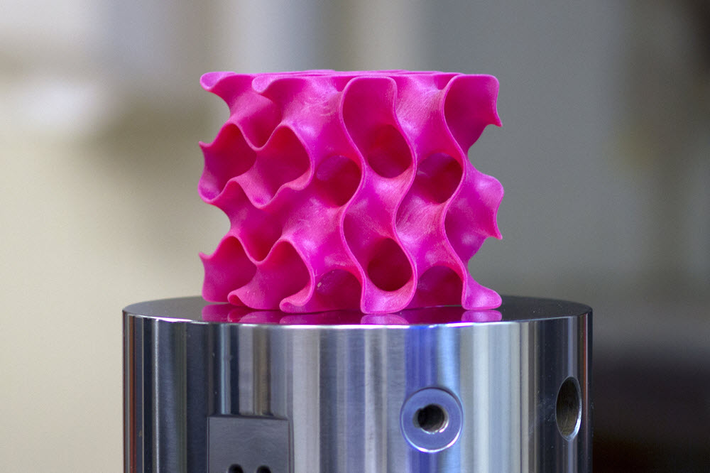
3-D-printed “gyroid” models such as this one were used to test the strength and mechanical properties of a new lightweight material (credit: Melanie Gonick/MIT)

MIT scientists said today they’ve just created one the strongest materials known (ten times stronger than steel, but also one of the lightest, with a density of just 5 percent of that of steel) by compressing and fusing flakes of graphene, a two-dimensional form of carbon.

In its two-dimensional form, graphene is thought to be the strongest of all known materials. But researchers until now have had a hard time translating that two-dimensional strength into useful three-dimensional materials.

It’s all about the geometrical configuration

But it’s not about the material itself; it’s about their unusual 3-D geometrical configuration, the researchers discovered. That suggests that similar strong, lightweight materials (in addition to graphene) could be made from a variety of materials by creating similar geometric features.

“You can replace the material itself with anything,” says Markus Buehler, the head of MIT’s Department of Civil and Environmental Engineering (CEE) and the McAfee Professor of Engineering. “The geometry is the dominant factor. It’s something that has the potential to transfer to many things.”

The findings were reported today an open-access paper in the journal Science Advances.

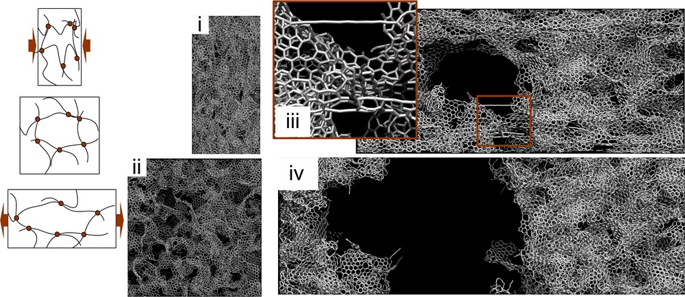
This illustration shows the simulation results of  compression (top left and i) and tensile (bottom left and ii) tests on 3-D graphene (credit: Zhao Qin)

By analyzing the material’s behavior down to the level of individual atoms within the structure, the engineers were able to produce a mathematical framework that very closely matches experimental observations.

Two-dimensional materials — basically flat sheets that are just one atom in thickness but can be indefinitely large in the other dimensions — have exceptional strength as well as unique electrical properties. But because of their extraordinary thinness, “they are not very useful for making 3-D materials that could be used in vehicles, buildings, or devices,” says Buehler. “What we’ve done is to realize the wish of translating these 2-D materials into three-dimensional structures.”

The trick: heat + pressure

The solution for compressing small flakes of graphene turned out to be a combination of heat and pressure. This process produced a strong, stable structure whose form resembles that of some corals and microscopic creatures called diatoms. These new shapes, which have an enormous surface area in proportion to their volume, proved to be remarkably strong.

Buehler says the process resembles what would happen with sheets of paper. Paper has little strength along its length and width, and can be easily crumpled up. But when made into certain shapes, for example rolled into a tube, suddenly the strength along the length of the tube is much greater and can support substantial weight. Similarly, the geometric arrangement of the graphene flakes after treatment naturally forms a very strong configuration.


Melanie Gonick/MIT | One of the strongest, lightweight materials known

Other applications

But many other possible applications of the material could eventually be feasible, the researchers say, for uses that require a combination of extreme strength and light weight. “You could either use the real graphene material or use the geometry we discovered with other materials, like polymers or metals,” Buehler says, to gain similar advantages of strength combined with advantages in cost, processing methods, or other material properties (such as transparency or electrical conductivity).

The unusual geometric shapes that graphene naturally forms under heat and pressure look something like a Nerf ball — round, but full of holes. These shapes, known as “gyroids,” are so complex that “actually making them using conventional manufacturing methods is probably impossible,” Buehler says.

The team used 3-D-printed models of the structure, enlarged to thousands of times their natural size, for testing purposes. For actual synthesis, the researchers say, one possibility is to use the polymer or metal particles as templates, coat them with graphene by chemical vapor deposit before heat and pressure treatments, and then chemically or physically remove the polymer or metal phases to leave 3-D graphene in the gyroid form.

The same geometry could even be applied to large-scale structural materials, they suggest. For example, concrete for a structure such a bridge might be made with this porous geometry, providing comparable strength with a fraction of the weight. This approach would have the additional benefit of providing good insulation because of the large amount of enclosed airspace within it.

Because the shape is riddled with very tiny pore spaces, the material might also find application in some filtration systems, for either water or chemical processing. The mathematical descriptions derived by this group could facilitate the development of a variety of applications, the researchers say.

The research was supported by the Office of Naval Research, the Department of Defense Multidisciplinary University Research Initiative, and BASF-North American Center for Research on Advanced Materials.

How to form the world’s smallest self-assembling nanowires — just 3 atoms wide

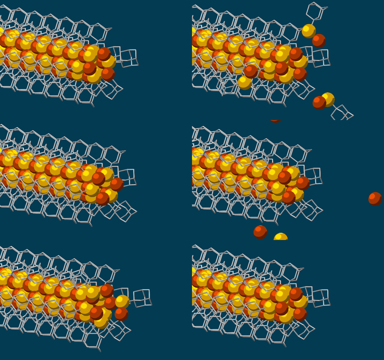
This animation shows molecular building blocks joining the tip of a growing self-assembling nanowire. Each block consists of a diamondoid — the smallest possible bit of diamond — attached to sulfur and copper atoms (yellow and brown spheres). Like LEGO blocks, they only fit together in certain ways that are determined by their size and shape. The copper and sulfur atoms form a conductive wire in the middle, and the diamondoids form an insulating outer shell. (credit: SLAC National Accelerator Laboratory)

Scientists at Stanford University and the Department of Energy’s SLAC National Accelerator Laboratory have discovered a way to use diamondoids* — the smallest possible bits of diamond — to self-assemble atoms, LEGO-style, into the thinnest possible electrical wires, just three atoms wide.

The new technique could potentially be used to build tiny wires for a wide range of applications, including fabrics that generate electricity, optoelectronic devices that employ both electricity and light, and superconducting materials that conduct electricity without any loss. The scientists reported their results last week in Nature Materials.

The researchers started with the smallest possible diamondoids —interlocking cages of carbon and hydrogen — and attached a sulfur atom to each. Floating in a solution, each sulfur atom bonded with a single copper ion — creating a semiconducting combination of copper and sulfur known as a chalcogenide.

A conventional insulated electrical copper wire (credit: Alibaba)

That created the basic nanowire building blocks, which then drifted toward each other, drawn by “unusually strong” van der Waals attraction between the diamondoids, and attached themselves to the growing tip of the nanowire. The attached diamondoids formed an insulating shell — creating the nanoscale equivalent of a conventional insulated electrical wire.

Although there are other ways to get materials to self-assemble, this is the first one shown to make a nanowire with a solid, crystalline core that has good electronic properties, said study co-author Nicholas Melosh, an associate professor at SLAC and Stanford and investigator with SIMES, the Stanford Institute for Materials and Energy Sciences at SLAC.

The team also included researchers from Lawrence Berkeley National Laboratory, the National Autonomous University of Mexico (UNAM) and Justus-Liebig University in Germany. The work was funded by the DOE Office of Science and the German Research Foundation.

* Found naturally in petroleum fluids, they are extracted and separated by size and geometry in a SLAC laboratory.


Citation: Yan et al., Nature Materials, 26 December 2016 (10.1038/nmat4823)

Press Office Contact: Andrew Gordon, agordon@slac.stanford.edu, (650) 926-2282


Abstract of Hybrid metal–organic chalcogenide nanowires with electrically conductive inorganic core through diamondoid-directed assembly

Controlling inorganic structure and dimensionality through structure-directing agents is a versatile approach for new materials synthesis that has been used extensively for metal–organic frameworks and coordination polymers. However, the lack of ‘solid’ inorganic cores requires charge transport through single-atom chains and/or organic groups, limiting their electronic properties. Here, we report that strongly interacting diamondoid structure-directing agents guide the growth of hybrid metal–organic chalcogenide nanowires with solid inorganic cores having three-atom cross-sections, representing the smallest possible nanowires. The strong van der Waals attraction between diamondoids overcomes steric repulsion leading to a cis configuration at the active growth front, enabling face-on addition of precursors for nanowire elongation. These nanowires have band-like electronic properties, low effective carrier masses and three orders-of-magnitude conductivity modulation by hole doping. This discovery highlights a previously unexplored regime of structure-directing agents compared with traditional surfactant, block copolymer or metal–organic framework linkers.

Nanoarray sniffs out and distinguishes ‘breathprints’ of multiple diseases

Schematic representation of the concept and design of the study, which involved collection of breath samples from 1404 patients diagnosed with one of 17 different diseases. One breath sample obtained from each subject was analyzed with the artificially intelligent nanoarray for disease diagnosis and classification (represented by patterns in the illustration), and a second sample was analyzed with gas chromatography–mass spectrometry to explore its chemical composition. (credit: Morad K. Nakhleh et al./ACS Nano)

An international team of 63 scientists in 14 clinical departments have identified a unique “breathprint” for 17 diseases with 86% accuracy and have designed a noninvasive, inexpensive, and miniaturized portable device that screens breath samples to classify and diagnose several types of diseases, they report in an open-access paper in the journal ACS Nano.

As far back as around 400 B.C., doctors diagnosed some diseases by smelling a patient’s exhaled breath, which contains nitrogen, carbon dioxide, oxygen, and a small amount of more than 100 other volatile chemical components. Relative amounts of these substances vary depending on the state of a person’s health. For example, diabetes creates a sweet breath smell. More recently, several teams of scientists have developed experimental breath analyzers, but most of these instruments focus on one disease, such as diabetes and melanoma, or a few diseases.

Detecting 17 diseases

The researchers developed an array of nanoscale sensors to detect the individual components in thousands of breath samples collected from 1404 patients who were either healthy or had one of 17 different diseases*, such as kidney cancer or Parkinson’s disease.

The team used mass spectrometry to identify the breath components associated with each disease. By analyzing the results with artificial intelligence techniques (binary classifiers), the team found that each disease produces a unique breathprint, based on differing amounts of 13 volatile organic chemical (VOC) components. They also showed that the presence of one disease would not prevent the detection of others — a prerequisite for developing a practical device to screen and diagnose various diseases.

Based on the research, the team designed an organic layer that functions as a sensing layer (recognition element) for adsorbed VOCs and an electrically conductive nanoarray based on resistive layers of molecularly modified gold nanoparticles and a random network of single-wall carbon nanotubes. The nanoparticles and nanotubes have different electrical conductivity patterns associated with different diseases.**

The authors received funding from the ERC and LCAOS of the European Union’s Seventh Framework Programme for Research and Technological Development, the EuroNanoMed Program under VOLGACORE, and the Latvian Council of Science.

* Lung cancer, colorectal cancer, head and neck cancer, ovarian cancer, bladder cancer, prostate cancer, kidney cancer, gastric cancer, Crohn’s disease, ulcerative colitis, irritable bowel syndrome, idiopathic Parkinson’s, atypical Parkinsonism, multiple sclerosis, pulmonary arterial hypertension, pre-eclampsia, and chronic kidney disease.

** During exposure to breath samples, interaction between the VOC components and the organic sensing layer changes the electrical resistance of the sensors. The relative change of sensor’s resistance at the peak (beginning), middle, and end of the exposure, as well as the area under the curve of the whole measurement were measured. All breath samples identified by the AI nanoarray were also examined using an independent lab-based analytical technique: gas chromatography linked with mass spectrometry.


Abstract of Diagnosis and Classification of 17 Diseases from 1404 Subjects via Pattern Analysis of Exhaled Molecules

We report on an artificially intelligent nanoarray based on molecularly modified gold nanoparticles and a random network of single-walled carbon nanotubes for noninvasive diagnosis and classification of a number of diseases from exhaled breath. The performance of this artificially intelligent nanoarray was clinically assessed on breath samples collected from 1404 subjects having one of 17 different disease conditions included in the study or having no evidence of any disease (healthy controls). Blind experiments showed that 86% accuracy could be achieved with the artificially intelligent nanoarray, allowing both detection and discrimination between the different disease conditions examined. Analysis of the artificially intelligent nanoarray also showed that each disease has its own unique breathprint, and that the presence of one disease would not screen out others. Cluster analysis showed a reasonable classification power of diseases from the same categories. The effect of confounding clinical and environmental factors on the performance of the nanoarray did not significantly alter the obtained results. The diagnosis and classification power of the nanoarray was also validated by an independent analytical technique, i.e., gas chromatography linked with mass spectrometry. This analysis found that 13 exhaled chemical species, called volatile organic compounds, are associated with certain diseases, and the composition of this assembly of volatile organic compounds differs from one disease to another. Overall, these findings could contribute to one of the most important criteria for successful health intervention in the modern era, viz. easy-to-use, inexpensive (affordable), and miniaturized tools that could also be used for personalized screening, diagnosis, and follow-up of a number of diseases, which can clearly be extended by further development.