Using graphene to detect brain cancer cells

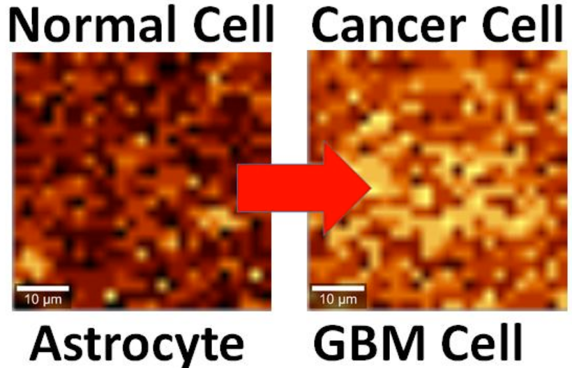
Brain cell culture. Left: Normal astrocyte brain cell; Right: cancerous Glioblastoma Multiforme (GBM) version, imaged by Raman spectrography. (credit: B. Keisham et al./ACS Appl. Mater. Interfaces)

By interfacing brain cells with graphene, University of Illinois at Chicago researchers have differentiated a single hyperactive Glioblastoma Multiforme cancerous astrocyte cell from a normal cell in the lab — pointing the way to developing a simple, noninvasive tool for early cancer diagnosis.

In the study, reported in the journal ACS Applied Materials & Interfaces, the researchers looked at lab-cultured human brain astrocyte cells taken from a mouse model. They compared normal astrocytes to their cancerous counterpart, highly malignant brain tumor glioblastoma multiforme.
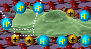
Illustration showing an astrocyte cell taken from a mouse brain draped over graphene (credit: B. Keisham et al./ACS Appl. Mater. Interfaces)

In a lab analysis, the cell is draped over graphene, explains Vikas Berry, associate professor and head of chemical engineering at UIC, who led the research along with Ankit Mehta, assistant professor of clinical neurosurgery in the UIC College of Medicine.

“The electric field around the cancer cell pushes away electrons in graphene’s electron cloud,” he said, which changes the vibration energy of the carbon atoms [in the graphene]. The change in vibration energy (resulting from the cancerous condition) can be pinpointed by Raman spectroscopy with a resolution of 300 nanometers, allowing for determining the activity of a single cell. (Raman spectroscopy is a highly sensitive method commonly used in chemistry to identify molecules by how they scatter laser light.)

“Graphene is the thinnest known material and is very sensitive to whatever happens on its surface,” Berry said. The nanomaterial is composed of a single layer of carbon atoms linked in a hexagonal chicken-wire pattern, and all the atoms share a cloud of electrons moving freely about the surface.

Patient biopsies planned

The technique is now being studied in a mouse model of cancer, with results that are “very promising,” Berry said. Experiments with patient biopsies would be further down the road. “Once a patient has brain tumor surgery, we could use this technique to see if the tumor relapses,” Berry said. “For this, we would need a cell sample we could interface with graphene and look to see if cancer cells are still present.”

The same technique may also work to differentiate between other types of cells or the activity of cells. “We may be able to use it with bacteria to quickly see if the strain is Gram-positive or Gram-negative,” Berry said. “We may be able to use it to detect sickle cells.”

Earlier this year, Berry and other coworkers introduced nanoscale ripples in graphene, causing it to conduct differently in perpendicular directions, useful for electronics. They wrinkled the graphene by draping it over a string of rod-shaped bacteria, then vacuum-shrinking the germs. “We took the earlier work and sort of flipped it over,” Berry said. “Instead of laying graphene on cells, we laid cells on graphene and studied graphene’s atomic vibrations.”

Funding was provided by UIC.


Abstract of Cancer Cell Hyperactivity and Membrane Dipolarity Monitoring via Raman Mapping of Interfaced Graphene: Toward Non-Invasive Cancer Diagnostics

Ultrasensitive detection, mapping, and monitoring of the activity of cancer cells is critical for treatment evaluation and patient care. Here, we demonstrate that a cancer cell’s glycolysis-induced hyperactivity and enhanced electronegative membrane (from sialic acid) can sensitively modify the second-order overtone of in-plane phonon vibration energies (2D) of interfaced graphene via a hole-doping mechanism. By leveraging ultrathin graphene’s high quantum capacitance and responsive phononics, we sensitively differentiated the activity of interfaced Glioblastoma Multiforme (GBM) cells, a malignant brain tumor, from that of human astrocytes at a single-cell resolution. GBM cell’s high surface electronegativity (potential ∼310 mV) and hyperacidic-release induces hole-doping in graphene with a 3-fold higher 2D vibration energy shift of approximately 6 ± 0.5 cm–1 than astrocytes. From molecular dipole-induced quantum coupling, we estimate that the sialic acid density on the cell membrane increases from one molecule per ∼17 nm2 to one molecule per ∼7 nm2. Furthermore, graphene phononic response also identified enhanced acidity of cancer cell’s growth medium. Graphene’s phonon-sensitive platform to determine interfaced cell’s activity/chemistry will potentially open avenues for studying activity of other cancer cell types, including metastatic tumors, and characterizing different grades of their malignancy.

How to enable soft robots to better mimick biological motions

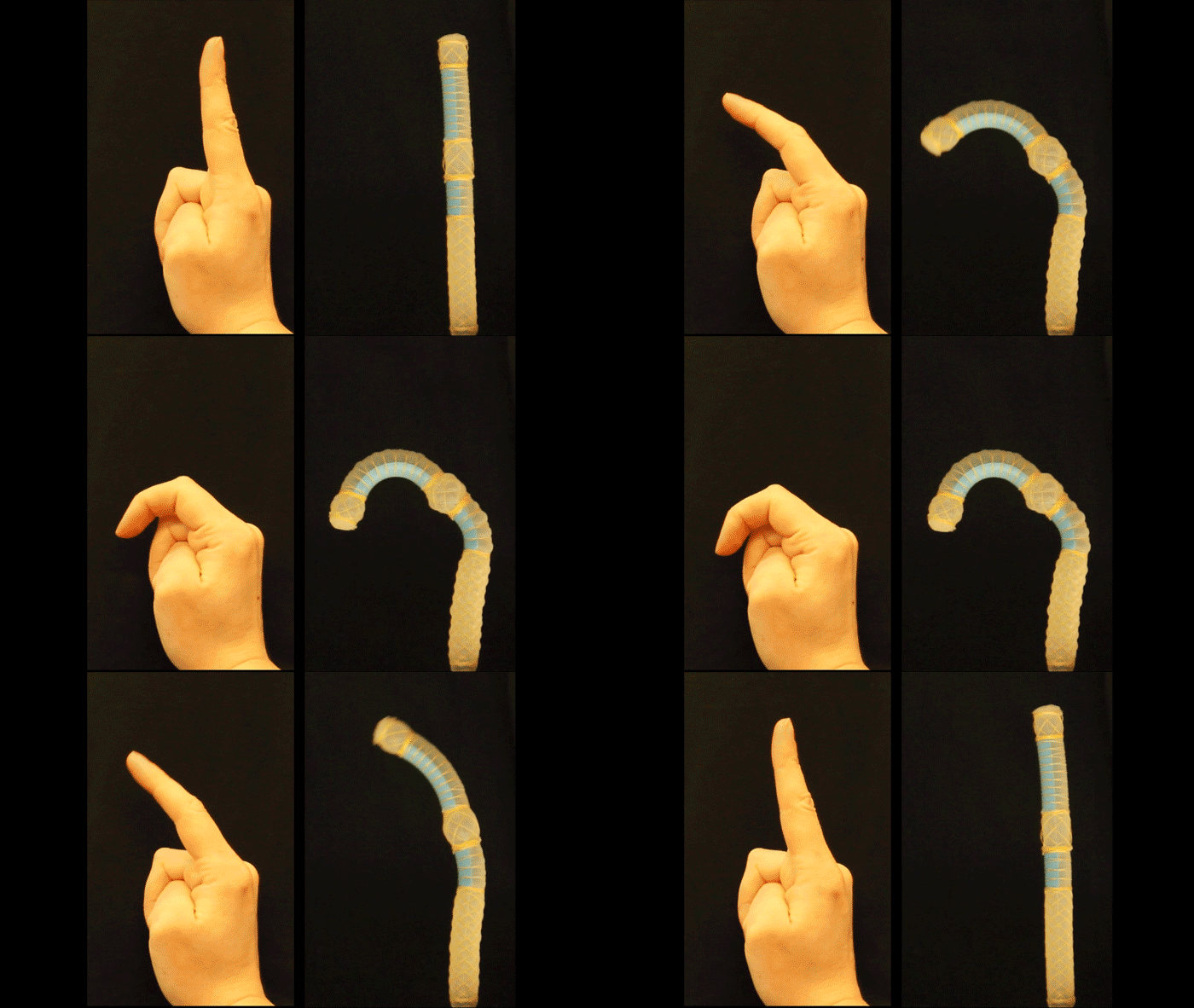
Researchers used mathematical modeling to optimize the design of an actuator to perform biologically inspired motions (credit: Harvard SEAS)

Harvard researchers have developed a method for automatically designing actuators that enable fingers and knees in a soft robot to move more organically, a robot arm to move more smoothly along a path, or a wearable robot or exoskeleton to help a patient move a limb more naturally.

Designing such actuators is currently a complex design challenge, requiring a sequence of actuator segments, each performing a different motion. “Rather than designing these actuators empirically, we wanted a tool where you could plug in a motion and it would tell you how to design the actuator to achieve that motion,” said Katia Bertoldi, the John L. Loeb Associate Professor of the Natural Sciences and coauthor of the paper.

Designing an actuator that replicates a complex input motion. (A) Analytical models of actuator segments that can extend, expand, twist, or bend are the first input to the design tool. (B) The second input to the design tool is the kinematics of the desired motion. (C) The design tool outputs the optimal segment lengths and fiber angles for replicating the input motion. (credit: Fionnuala Connoll et al./PNAS)

The method developed by the team uses mathematical modeling of fluid-powered, fiber-reinforced actuators that can produce a wide range of motions. It optimizes the actuator design for performing specific motions (kinematics), different geometries, material properties, and pressure required for extending, expanding, twisting, and bending.

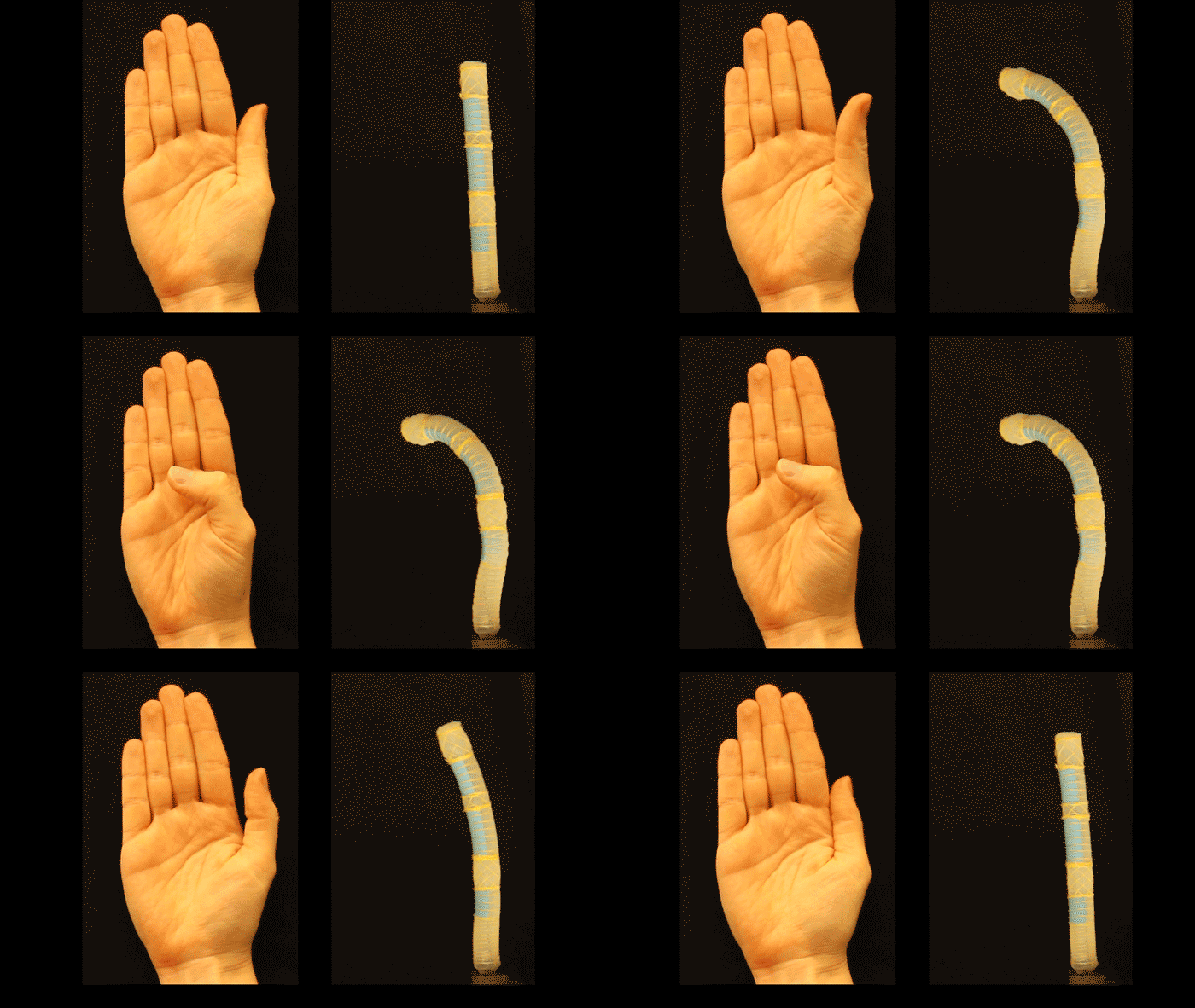
This soft actuator twists like a thumb when powered by a single pressure source (credit: Harvard SEAS)

The researchers from the Harvard John A. Paulson School of Engineering and Applied Sciences (SEAS) and the Wyss Institute for Biologically Inspired Engineering tested the model by designing a soft robot that bends like an index finger and twists like a texting thumb when powered by a single pressure source.

The research was published this week in the journal Proceedings of the National Academy of Sciences. “Future work will also focus on developing a model that combines bending with other motions, to increase the versatility of the algorithm,” the authors note in the paper.

In a future robot design, the model could conceivably be integrated with Cornell University’s design for soft, stretchable optoelectronic sensors in fingers that detect shape and texture.

The new methodology will be included in the Soft Robotic Toolkit, an online, open-source resource developed at SEAS to assist researchers, educators and budding innovators to design, fabrication, model, characterize and control their own soft robots.


Abstract of Automatic design of fiber-reinforced soft actuators for trajectory matching

Soft actuators are the components responsible for producing motion in soft robots. Although soft actuators have allowed for a variety of innovative applications, there is a need for design tools that can help to efficiently and systematically design actuators for particular functions. Mathematical modeling of soft actuators is an area that is still in its infancy but has the potential to provide quantitative insights into the response of the actuators. These insights can be used to guide actuator design, thus accelerating the design process. Here, we study fluid-powered fiber-reinforced actuators, because these have previously been shown to be capable of producing a wide range of motions. We present a design strategy that takes a kinematic trajectory as its input and uses analytical modeling based on nonlinear elasticity and optimization to identify the optimal design parameters for an actuator that will follow this trajectory upon pressurization. We experimentally verify our modeling approach, and finally we demonstrate how the strategy works, by designing actuators that replicate the motion of the index finger and thumb.

A robotic hand with a human’s delicate sense of touch

A soft, sensitive robotic hand mounted on a robotic arm (credit: Cornell University)

Cornell University engineers have invented a new kind of robotic hand with a human’s delicate sense of touch.

Scenario: you lost part of your arm in a car accident. That artificial arm and hand you got from the hospital lets you feel and pick up things — even type on a keyboard. But not with the same sensitivity as a real hand. Now, an artificial prosthesis can even let you feel which one of three tomatoes is ripe (as shown in the video below).

The engineers’ trick was to use soft, stretchable optoelectronic (light + electronics) sensors in the fingers to detect shape and texture. (The sensors in existing prosthetic and robot hands use cruder tactile, or touch, sensors with bulky, rigid motors to measure strain.) The new prosthetic hand is a lot more sensitive. It can measure softness or hardness, how much the material stretches when touched, and how much force needs to be supplied to make the material deform.

How to make an (almost) human hand

A Cornell group led by Robert Shepherd, assistant professor of mechanical and aerospace engineering and principal investigator of Organic Robotics Lab, has published a paper describing this research in the debut edition of the journal Science Robotics (open access until Jan. 31).

Schematic of prosthetic hand structure and components (credit: Cornell University)

Unlike existing prosthetic and robot sensors, these sensors are integrated within the hand (instead of on the surface), so they can actually detect forces being transmitted through the thickness of the robot hand — simulating how a human hand feels. The more the prosthetic hand deforms (as it touches an object), the more light is lost. That variable loss of light, as detected by the photodiode, is what allows the prosthetic hand to “sense” its surroundings with high sensitivity and discrimination.*

This work was supported by a grant from Air Force Office of Scientific Research, and made use of the Cornell NanoScale Science and Technology Facility and the Cornell Center for Materials Research, both of which are supported by the National Science Foundation.

* The optoelectronic sensors are based on novel elastomeric optical waveguides, using a 3D-printed mold and a soft-lithography process to create a fluidically powered, stretchable material. Each high-precision waveguide incorporates an LED to generate light and a photodiode to measure the amount of light lost (which depends dynamically on the curvature, elongation, and force of the prosthetic hand).

To make the hand, Shepherd’s group used a four-step soft lithography process to produce the inside of the hand (core) and the cladding (outer surface of the waveguide), which also houses the LED (light-emitting diode) and the photodiode (light detector).


CNBC International | Scientists build a robotic hand with a soft touch | CNBC International


Abstract of Optoelectronically innervated soft prosthetic hand via stretchable optical waveguides

Because of their continuous and natural motion, fluidically powered soft actuators have shown potential in a range of robotic applications, including prosthetics and orthotics. Despite these advantages, robots using these actuators require stretchable sensors that can be embedded in their bodies for sophisticated functions. Presently, stretchable sensors usually rely on the electrical properties of materials and composites for measuring a signal; many of these sensors suffer from hysteresis, fabrication complexity, chemical safety and environmental instability, and material incompatibility with soft actuators. Many of these issues are solved if the optical properties of materials are used for signal transduction. We report the use of stretchable optical waveguides for strain sensing in a prosthetic hand. These optoelectronic strain sensors are easy to fabricate, are chemically inert, and demonstrate low hysteresis and high precision in their output signals. As a demonstration of their potential, the photonic strain sensors were used as curvature, elongation, and force sensors integrated into a fiber-reinforced soft prosthetic hand. The optoelectronically innervated prosthetic hand was used to conduct various active sensation experiments inspired by the capabilities of a real hand. Our final demonstration used the prosthesis to feel the shape and softness of three tomatoes and select the ripe one.

Triggered by ultrasound, microbubbles open the blood-brain barrier to administer drugs without harming other areas of the body

Microbubbles containing a new fluorescent substance in their lipid coating, released in a designated point in the brain by ultrasound (credit: C. Sierra et al./Columbia University UEIL)

Using ultrasound to bypass the blood-brain barrier (BBB), Columbia University researchers have succeeded in releasing drugs only in the specific area of the brain where they are needed — not in the rest of the body. The goal is to help treat Parkinson’s, Alzheimer’s, and other neurodegenerative diseases without collateral damage.

The BBB is an impassable obstacle for 98% of drugs, which it treats as pathogens and blocks them from passing from patients’ bloodstream into the brain. Using ultrasound (sound whose frequency is higher than the range of human hearing), drugs can administered using an intravenous injection of innocuous lipid-coated gas microbubbles. That technique was perfected by Columbia University scientists, who reported their research in 2011 in PNAS and in 2014 in the Journal of Cerebral Blood Flow & Metabolism.

Microbubble (credit: C. Sierra et al./Journal of Cerebral Blood Flow & Metabolism)

With this method, ultrasound is focused on a specific region of the brain, causing the microbubbles to oscillate and increase in size and expand. When they reach the critical size of 8 microns, the blood–brain barrier near them opens, allowing the medicine circulating in the blood to pass through.

This technique has been used experimentally for over ten years, but has had a disadvantage: at excessive pressure, the microbubbles can suddenly collapse, so there is no lipid shell to retain the covering of  the microbubbles, allowing the contained drug to flow through the blood pool and causing microdamage to the cerebral vessels and elsewhere.

Now, scientists at the Ultrasound Elasticity Imaging Laboratory (UEIL) at Columbia University have taken a major step forward by incorporating a fluorescent molecule called 5-dodecanoylaminofluorescein into the lipid coating of the microbubbles.

This molecule allows the scientists to determine the optimal pressure to prevent bursting of the microbubbles*, according to UEIL physicist Carlos Sierra and lead author of a paper on this new finding published in the current issue of Journal of Cerebral Blood Flow & Metabolism.

Human trials planned

So far, the researchers have proven the efficacy of their technique on mice, confirming that this molecule was reaching the brain without affecting other parts of the animal. They also identified the acoustic pressure thresholds at which the substance is guaranteed to safely reach its target in vivo.

“Defining these parameters means we can think about how to transfer the technique to human patients, although it has to be tested on monkeys first,” Sierra explains. “It could be applied to diseases like Parkinson’s, Alzheimer’s, Huntington’s diseases, brain tumors, strokes, multiple sclerosis, and amyotrophic lateral sclerosis, where we expect to see a very significant rise in the efficacy of treatment and a considerable reduction in side effects.”

Sierra is funded by a grant from Berrié Foundation in Spain.

* By ex vivo fluorescence imaging and by in vivo transcranial passive cavitation detection.


Abstract of Lipid microbubbles as a vehicle for targeted drug delivery using focused ultrasound-induced blood–brain barrier opening

Focused ultrasound in conjunction with lipid microbubbles has fully demonstrated its ability to induce non-invasive, transient, and reversible blood–brain barrier opening. This study was aimed at testing the feasibility of our lipid-coated microbubbles as a vector for targeted drug delivery in the treatment of central nervous system diseases. These microbubbles were labeled with the fluorophore 5-dodecanoylaminfluorescein. Focused ultrasound targeted mouse brains in vivo in the presence of these microbubbles for trans-blood–brain barrier delivery of 5-dodecanoylaminfluorescein. This new approach, compared to previously studies of our group, where fluorescently labeled dextrans and microbubbles were co-administered, represents an appreciable improvement in safety outcome and targeted drug delivery. This novel technique allows the delivery of 5-dodecanoylaminfluorescein at the region of interest unlike the alternative of systemic exposure. 5-dodecanoylaminfluorescein delivery was assessed by ex vivo fluorescence imaging and by in vivo transcranial passive cavitation detection. Stable and inertial cavitation doses were quantified. The cavitation dose thresholds for estimating, a priori, successful targeted drug delivery were, for the first time, identified with inertial cavitation were concluded to be necessary for successful delivery. The findings presented herein indicate the feasibility and safety of the proposed microbubble-based targeted drug delivery and that, if successful, can be predicted by cavitation detection in vivo.


Implantable device targets cancer, other illnesses with controlled long-term drug delivery

A drug-delivery capsule directly implanted into a cancerous tumor (credit: Lyle Hood/UTSA)

A new drug-delivery system based on an tiny implantable capsule could “revolutionize” the delivery of medicine to treat cancer and a host of other diseases and ailments, according to researchers at The University of Texas at San Antonio (UTSA).

“The problem with most drug-delivery systems is that you have a specific minimum dosage of medicine that you need to take for it to be effective,” said Lyle Hood, assistant professor of mechanical engineering. “There’s also a limit to how much of the drug can be present in your system so that it doesn’t make you sick.” So a person who needs frequent doses of a specific medicine is required to take a pill every day or visit a doctor for injections.

KurzweilAI has covered a number of drug-delivery systems targeting cancer this year, based on “Nanoparticle cluster bombs,” “magnetically guided bacteria,” and “DNA-based lock-and-key pores,” for example.

What makes the UTSA system different is that it’s an implantable capsule, filled with medicinal fluid that uses about 5000 nanochannels to regulate the rate of release of the medicine, Hood explained. “This way, we have the proper amount of drugs in a person’s system to be effective, but not so much that they’ll harm that person.”

The capsule can deliver medicinal doses for several days or a few weeks, says Hood, and can be used for any kind of ailment that needs a localized delivery over several days or a few weeks. He believes this makes it especially tailored for treating cancer.

A larger version of the device, originally created by Alessandro Grattoni, chair of the Department of Nanomedicine at Houston Methodist Research Institute, can treat diseases like HIV for up to a year. “In HIV treatment, you can bombard the virus with drugs to the point that that person is no longer infectious and shows no symptoms,” Hood said. “The danger is that if that person stops taking their drugs, the amount of medicine in his or her system drops below the effective dose and the virus is able to become resistant to the treatments.”

The new capsule could provide a constant delivery of the HIV-battling drugs to prevent such an outcome. Hood noted it can also be used to deliver cortisone to damaged joints to avoid painful, frequent injections, and possibly even to pursue immunotherapy treatments for cancer patients.

“The idea behind immunotherapy is to deliver a cocktail of immune drugs to call attention to the cancer in a person’s body, so the immune system will be inspired to get rid of the cancer itself,” he added.

The current prototype of the device is permanent and injected under the skin, but the researchers are working on 3-D printing technology to make a new, fully biodegradable version of the device that could potentially be swallowed.


Abstract of Nanochannel Implants for Minimally-Invasive Insertion and Intratumoral Delivery

Novel approaches to achieve local, intratumoral drug delivery have the dual benefit of reducing systemic toxicity while enhancing efficacy for malignant cells. We have developed a new implantable system combining a next-generation BioNEMS nanofluidic membrane with parallel nanochannels that offers controlled release of biomolecules. Based on concentration-driven diffusive transport, nanochannel membranes provide a “drug agnostic” delivery mechanism. Integrating this nanotechnology within a small implantable capsule permits multipurpose functionality and compatibility with different therapeutic approaches as well as diagnostic imaging capability. A minimally-invasive, percutaneous trocar delivery mechanism enables serial implantation throughout a target tissue volume. In this manuscript, we demonstrate that this platform is capable of sustained delivery for chemotherapy, radiosensitization, immunomodulation, and imaging contrast, among others. This platform’s utility was established through release of doxorubicin, OX86, FGK45, and Magnevist. Further proof-of-concept experiments demonstrated successful in vivo implantation and intratumoral release of antibodies and contrast agents, as well as the platform’s MR-compatibility and capability as a radiopaque fiducial. These results provide strong evidence for a flexible, multifunctional nanofluidic implant capable of broadening local delivery utility in the clinic.

Battery breakthrough charges in seconds, lasts for a week

Illustration representing the novel design of a hybrid supercapacitor, showing bundles of nanowires (blue) coated with 2D energy-storage materials (yellow) (credit: University of Central Florida)

University of Central Florida researchers have developed a radical new supercapacitor design that could one day replace lithium-ion batteries, allowing users to charge a mobile phone in a few seconds and with a charge that lasts a week, according to the researchers. The new battery would be flexible and a fraction of the size of a lithium-ion battery.

The proof-of-concept design is based on a hybrid supercapacitor composed of a core with millions of highly conductive nanowires coated with shells of two-dimensional materials.* It combines fast charging and discharging (high power density) and high storage capacity (high energy density).

Supercapacitor design: an array of electrically conductive nanowires (orange) with metal current-collector covering (blue) (credit: Nitin Choudhary et al./ACS Nano)

Optical image of core/shell nanowires on a tungsten foil under mechanical bending (left). Corresponding SEM image (right) shows high-density, well-aligned nanowires along with their faceted surface (inset). The scale bar in the inset is 500 nm. (credit: Nitin Choudhary et al./ACS Nano)

Another advantage would be “cyclic stability” (how many times a battery can be charged, drained and recharged before beginning to degrade). A lithium-ion battery can be recharged fewer than 1,500 times without significant failure, compared to recently developed supercapacitors based on two-dimensional materials, which can be recharged more than 30,000 times.

Supercapacitor prototype showing flexible design (credit: (credit: University of Central Florida)

Electric vehicles could also benefit from longer-range operation and sudden bursts of power and speed. The flexible material could mean a significant advancement in wearable tech, according to the researchers, and would also avoid the risk of overheating and explosion with lithium-ion batteries.

Hee-Suk Chung of Korea Basic Science Institute was also involved in the research, which was published recently in the journal ACS Nano.

* The core nanowire material is tungsten trioxide (WO3) and the two-dimensional shell material is a transition-metal dichalcogenide, tungsten disulfide (WS2).

Ragone plot to compare the performances of various technologies with the core/shell nanowires supercapacitor in this study (credit: Nitin Choudhary et al./ACS Nano)

Galvanostatic Charging/Discharging (GCD) various current densities in the voltage range of 0.3 and 0.5 V, showing nearly symmetrical voltage curves, indicating highly reversible and fast responses. (credit: Nitin Choudhary et al./ACS Nano)


Abstract of High-Performance One-Body Core/Shell Nanowire Supercapacitor Enabled by Conformal Growth of Capacitive 2D WS2 Layers

Two-dimensional (2D) transition-metal dichalcogenides (TMDs) have emerged as promising capacitive materials for supercapacitor devices owing to their intrinsically layered structure and large surface areas. Hierarchically integrating 2D TMDs with other functional nanomaterials has recently been pursued to improve electrochemical performances; however, it often suffers from limited cyclic stabilities and capacitance losses due to the poor structural integrity at the interfaces of randomly assembled materials. Here, we report high-performance core/shell nanowire supercapacitors based on an array of one-dimensional (1D) nanowires seamlessly integrated with conformal 2D TMD layers. The 1D and 2D supercapacitor components possess “one-body” geometry with atomically sharp and structurally robust core/shell interfaces, as they were spontaneously converted from identical metal current collectors via sequential oxidation/sulfurization. These hybrid supercapacitors outperform previously developed any stand-alone 2D TMD-based supercapacitors; particularly, exhibiting an exceptional charge–discharge retention over 30,000 cycles owing to their structural robustness, suggesting great potential for unconventional energy storage technologies.

‘Atomic sandwich’ computing material uses 100 times less energy

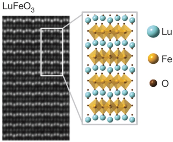
New magnetoelectric multiferroic material operates at 100 times lower power (credit: Julia A. Mundy/Nature)

Lawrence Berkeley National Laboratory scientists have developed a new “magnetoelectric multiferroic*” material that could lead to a new generation of computing devices with more computing power while consuming a fraction of the energy that today’s electronics require.

Electronics could be half of our total global energy consumption by 2030

“Electronics are the fastest-growing consumer of energy worldwide,” said Ramamoorthy Ramesh, associate laboratory director for energy technologies at Lawrence Berkeley National Laboratory.

“Today, about five percent of our total global energy consumption is spent on electronics, and that’s projected to grow to 40–50 percent by 2030 if we continue at the current pace and if there are no major advances in the field that lead to lower energy consumption.”

Global or world energy consumption is the total energy used by all of human civilization. The U.S. Energy Information Administration estimates that in 2013, world energy consumption was 157,481 terawatt hours (TWh), mainly from polluting expendables — oil, coal, and natural gas.

The new material, which combines electrical and magnetic properties at room temperature, could help reduce this consumption in the future.

Room-temperature multiferroics

The newly developed material sandwiches together individual layers of atoms, producing a thin film with magnetic polarity that can be “flipped” from positive to negative or vice versa with small pulses of electricity.

In the future, device makers could use this property to store digital 0’s and 1’s, the binary backbone that underpins computing devices.

“Before this work, there was only one other room-temperature multiferroic whose magnetic properties could be controlled by electricity,” said John Heron, assistant professor in the Department of Materials Science and Engineering at the University of Michigan, who worked on the material with researchers at Cornell University. “That electrical control is what excites electronics makers, so this is a huge step forward.”

100 times less power required

Room-temperature multiferroics are a hotly pursued goal in the electronics field because they require much less power to read and write data than today’s semiconductor-based devices. In addition, they are nonvolatile (their data doesn’t vanish when the power is shut off).

Those properties could enable devices that require only brief pulses of electricity instead of the constant stream that’s needed for current electronics, resulting in using an estimated 100 times less energy.

To create the new material, the researchers started with thin, atomically precise films of hexagonal lutetium iron oxide (LuFeO3), a material known to be a robust ferroelectric, but not strongly magnetic. Lutetium iron oxide consists of alternating monolayers of lutetium oxide and iron oxide. They then used a technique called molecular-beam epitaxy (which takes place in a high vacuum) to add one extra monolayer of iron oxide to every 10 atomic repeats of the single-single monolayer pattern.

“We were essentially spray painting individual atoms of iron, lutetium and oxygen to achieve a new atomic structure that exhibits stronger magnetic properties,” said Darrell Schlom, a materials science and engineering professor at Cornell and senior author of a paper on the work recently published in Nature.

The result was a new material that combines a phenomenon in lutetium oxide called “planar rumpling” with the magnetic properties of iron oxide to achieve multiferroic properties at room temperature.**

While Heron believes a viable multiferroic device is likely several years off, the work puts the field closer to its goal of devices that continue the computing industry’s speed improvements while consuming less power — replacing current silicon-based technology.

The research was published in a paper in the Sept. 22 issue of Nature. It was supported by the Department of Energy’s Office of Science.

* The magnetoelectric effect is the phenomenon of inducing magnetic or electric polarization by applying an external electric or magnetic field. “Ferroics” is the generic name given to the study of iron-based ferromagnetsferroelectrics, and ferroelastics. These materials exhibit large changes in physical characteristics that occur when phase transitions (such as paramagnetic, or temporary magnetism, to ferromagnetic, or permanent magnetism) take place around some critical temperature value. Multiferroics exhibit more than one ferroic property simultaneously.

** Heron explains that the lutetium exhibits atomic-level displacements called rumples. Visible under an electron microscope, the rumples enhance the magnetism in the material, allowing it to persist at room temperature. The rumples can be moved by applying an electric field, and are enough to nudge the magnetic field in the neighboring layer of iron oxide from positive to negative or vice versa, creating a material whose magnetic properties can be controlled with electricity — a “magnetoelectric multiferroic.”


Abstract of Atomically engineered ferroic layers yield a room-temperature magnetoelectric multiferroic

Materials that exhibit simultaneous order in their electric and magnetic ground states hold promise for use in next-generation memory devices in which electric fields control magnetism. Such materials are exceedingly rare, however, owing to competing requirements for displacive ferroelectricity and magnetism. Despite the recent identification of several new multiferroic materials and magnetoelectric coupling mechanisms, known single-phase multiferroics remain limited by antiferromagnetic or weak ferromagnetic alignments, by a lack of coupling between the order parameters, or by having properties that emerge only well below room temperature, precluding device applications2. Here we present a methodology for constructing single-phase multiferroic materials in which ferroelectricity and strong magnetic ordering are coupled near room temperature. Starting with hexagonal LuFeO3—the geometric ferroelectric with the greatest known planar rumpling—we introduce individual monolayers of FeO during growth to construct formula-unit-thick syntactic layers of ferrimagnetic LuFe2O4 within the LuFeO3 matrix, that is, (LuFeO3)m/(LuFe2O4)1 superlattices. The severe rumpling imposed by the neighbouring LuFeO3 drives the ferrimagnetic LuFe2O4 into a simultaneously ferroelectric state, while also reducing the LuFe2O4 spin frustration. This increases the magnetic transition temperature substantially—from 240 kelvin for LuFe2O4to 281 kelvin for (LuFeO3)9/(LuFe2O4)1. Moreover, the ferroelectric order couples to the ferrimagnetism, enabling direct electric-field control of magnetism at 200 kelvin. Our results demonstrate a design methodology for creating higher-temperature magnetoelectric multiferroics by exploiting a combination of geometric frustration, lattice distortions and epitaxial engineering.

Engineers reveal fabrication process for revolutionary transparent graphene neural sensors

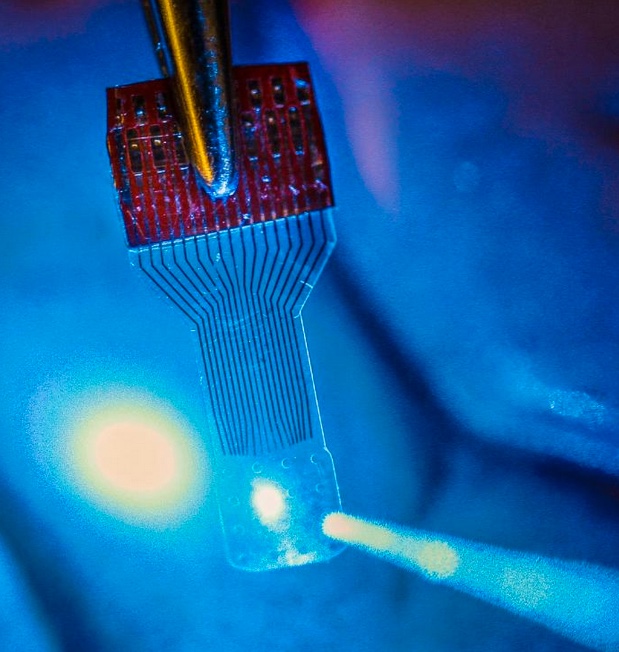
A blue light shines through a transparent, implantable medical sensor onto a brain. The invention may help neural researchers better view brain activity. (credit: Justin Williams research group)

In an open-access paper published Thursday (Oct. 13, 2016) in the journal Nature Protocols, University of Wisconsin–Madison engineers have published details of how to fabricate and use neural microelectrocorticography (μECoG) arrays made with transparent graphene in applications in electrophysiology, fluorescent microscopy, optical coherence tomography, and optogenetics.

Graphene is one of the most promising candidates for transparent neural electrodes, because the material has a UV to IR transparency of more than 90%, in addition to its high electrical and thermal conductivity, flexibility, and biocompatibility, the researchers note in the paper. That allows for simultaneous high-resolution imaging and optogenetic control.

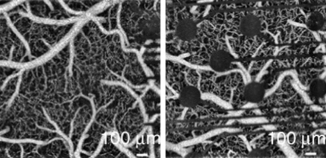
Left: Optical coherence tomography (OCT) image captured through an implanted transparent graphene electrode array, allowing for simultaneous observation of cells immediately beneath electrode sites during optical or electrical stimulation. Right: Optical coherence tomography (OCT) image taken with an implanted conventional opaque platinum electrode array. (credit: Dong-Wook Park et al./Nature Protocols)

The procedures in the paper are for a graphene μECoG electrode array implanted on the surface of the cerebral cortex and can be completed within 3–4 weeks by an experienced graduate student, according to the researchers. But this protocol “may be amenable to fabrication and testing of a multitude of other electrode arrays used in biological research, such as penetrating neural electrode arrays to study deep brain, nerve cuffs that are used to interface with the peripheral nervous system (PNS), or devices that interface with the muscular system,” according to the paper.

The researchers first announced the breakthrough in the open-access journal Nature Communications in 2014, as KurzweilAI reported. Now, the UW–Madison researchers are looking at ways to improve and build upon the technology. They also are seeking to expand its applications from neuroscience into areas such as research of stroke, epilepsy, Parkinson’s disease, cardiac conditions, and many others. And they hope other researchers do the same.

Funding for the initial research came from the Reliable Neural-Interface Technology program at the U.S. Defense Advanced Research Projects Agency.

The research was led by Zhenqiang (Jack) Ma, the Lynn H. Matthias Professor and Vilas Distinguished Achievement Professor in electrical and computer engineering at UW–Madison and Justin Williams, the Vilas Distinguished Achievement Professor in biomedical engineering and neurological surgery at UW–Madison.

Researchers at the University of Wisconsin-Milwaukee, Medtronic PLC Neuromodulation, the University of Washington, and Mahidol University in Bangkok, Thailand were also involved.


Abstract of Fabrication and utility of a transparent graphene neural electrode array for electrophysiology, in vivo imaging, and optogenetics

Transparent graphene-based neural electrode arrays provide unique opportunities for simultaneous investigation of electrophysiology, various neural imaging modalities, and optogenetics. Graphene electrodes have previously demonstrated greater broad-wavelength transmittance (~90%) than other transparent materials such as indium tin oxide (~80%) and ultrathin metals (~60%). This protocol describes how to fabricate and implant a graphene-based microelectrocorticography (μECoG) electrode array and subsequently use this alongside electrophysiology, fluorescence microscopy, optical coherence tomography (OCT), and optogenetics. Further applications, such as transparent penetrating electrode arrays, multi-electrode electroretinography, and electromyography, are also viable with this technology. The procedures described herein, from the material characterization methods to the optogenetic experiments, can be completed within 3–4 weeks by an experienced graduate student. These protocols should help to expand the boundaries of neurophysiological experimentation, enabling analytical methods that were previously unachievable using opaque metal–based electrode arrays.

Berkeley Lab announces first transistor with a working 1-nanometer gate

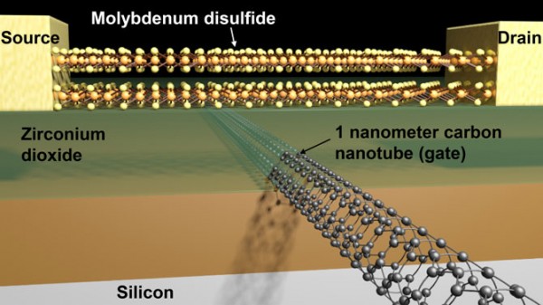
Schematic of a transistor with molybdenum disulfide semiconductor and 1-nanometer carbon nanotube gate. (credit: Sujay Desai/Berkeley Lab)

The first transistor with a working 1-nanometer (nm) gate* has been created by a team led by Lawrence Berkeley National Laboratory (Berkeley Lab) scientists. Until now, a transistor gate size less than 5 nanometers has been considered impossible because of quantum tunneling effects. (One nanometer is the diameter of a glucose molecule.)

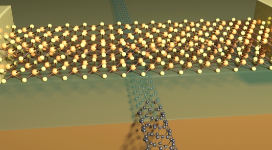
The breakthrough was achieved by creating a 2D (flat) semiconductor field-effect transistor using molybdenum disulfide (MoS2) instead of silicon and a 1D single-walled carbon nanotube (SWCNT) as a gate electrode, instead of various metals. (SWCNTs are hollow cylindrical tubes with diameters as small as 1 nanometer.)

The MoS2 advantage

Compared with MoS2, electrons flowing through silicon are lighter and encounter less resistance . But with a gate length below 5 nanometers in length, a quantum mechanical phenomenon called tunneling kicks in, and the gate barrier is no longer able to keep the electrons from barging through from the source to the drain terminals, so the transistor cannot be turned off.

Electrons flowing through MoS2 are heavier, so their flow can be controlled with smaller gate lengths. MoS2 can also be scaled down to atomically thin sheets, about 0.65 nanometers thick, with a a larger band gap and lower dielectric constant, a measure reflecting the ability of a material to store energy in an electric field (similar to a capacitor). These properties help improve the control of the flow of current inside the transistor when the gate length is reduced to 1 nanometer.

Transistors consist of three terminals: a source (left), a drain (right), and a gate (the carbon nanotube, black, below). Current flows through the semiconductor (MoS2, represented by the yellow molecular model) from the source to the drain. Based on the voltage applied to the gate, it switches the channel (the portion of the MoS2 semiconductor just above the carbon nanotube) on and off, via a dielectric (zirconium oxide, green), operating in a manner similar to a capacitor. (credit: Sujay Desai/Berkeley Lab)

“We made the smallest transistor reported to date,” said faculty scientist Ali Javey at the Department of Energy’s Lawrence Berkeley National Laboratory (Berkeley Lab) and lead principal investigator of the Electronic Materials program in Berkeley Lab’s Materials Science Division. “The gate length is considered a defining dimension of the transistor. We demonstrated a 1-nanometer-gate transistor, showing that with the choice of proper materials, there is a lot more room to shrink our electronics.”

The development could be key to keeping alive Intel co-founder Gordon Moore’s prediction that the density of transistors on integrated circuits would double every two years, enabling the increased performance of our laptops, mobile phones, televisions, and other electronics.

“The semiconductor industry has long assumed that any gate below 5 nanometers wouldn’t work, so anything below that was not even considered,” said study lead author Sujay Desai, a graduate student in Javey’s lab. “This research shows that sub-5-nanometer gates should not be discounted. Industry has been squeezing every last bit of capability out of silicon. By changing the material from silicon to MoS2, we can make a transistor with a gate that is just 1 nanometer in length, and operate it like a switch.”

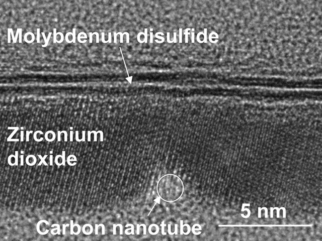
Transmission electron microscope image of a cross section of the transistor, showing the edge of a 1-nanometer carbon nanotube gate and the molybdenum disulfide semiconductor separated by zirconium dioxide, which is a dielectric insulator. (credit: Sujay B. Desai/Science)

Continuing Moore’s law

“This work demonstrated the shortest transistor ever,” said Javey, who is also a UC Berkeley professor of electrical engineering and computer sciences. “However, it’s a proof of concept. We have not yet packed these transistors onto a chip, and we haven’t done this billions of times over. We also have not developed self-aligned fabrication schemes for reducing parasitic resistances in the device. But this work is important to show that we are no longer limited to a 5-nanometer gate for our transistors. Moore’s Law can continue a while longer by proper engineering of the semiconductor material and device architecture.”

The findings appeared in the Oct. 7 issue of the journal Science. Researchers at the University of Texas at Dallas, Stanford University, and  the University of California, Berkeley, were also involved. The work at Berkeley Lab was primarily funded by the Department of Energy’s Basic Energy Sciences program.

According to an earlier article in CTimes on Sept. 30, Taiwan Semiconductor Manufacturing Co., Ltd. (TSMC) said the company is working toward a 1-nanometer manufacturing process, starting with a “5 nanometers process technology, while putting about 300 to 400 R&D personnel in developing more advanced 3-nanometer process.” However, TSMC spokesperson Elizabeth Sun told KurzweilAI that “no further information regarding any technology either under development or in path-finding stage will be disclosed to the public at this point.”

* Gate length is the length of the gate portion of the transistor, not to be confused with “node,” which was initially a measure of “half pitch” (half of the distance between features of a transistor), but the number itself has lost the exact meaning it once held. Gate length was 26nm for the 22nm node from Intel and 20 nanometers for the more recent 14nm node from Intel. — S. Natarajan et al., “A 14nm logic technology featuring 2nd-generation FinFET, air-gapped interconnects, self-aligned double patterning and a 0.0588 µm2 SRAM cell size,” 2014 IEEE International Electron Devices Meeting, San Francisco, CA, 2014, pp. 3.7.1-3.7.3. doi: 10.1109/IEDM.2014.7046976


Abstract of MoS2 transistors with 1-nanometer gate lengths

Scaling of silicon (Si) transistors is predicted to fail below 5-nanometer (nm) gate lengths because of severe short channel effects. As an alternative to Si, certain layered semiconductors are attractive for their atomically uniform thickness down to a monolayer, lower dielectric constants, larger band gaps, and heavier carrier effective mass. Here, we demonstrate molybdenum disulfide (MoS2) transistors with a 1-nm physical gate length using a single-walled carbon nanotube as the gate electrode. These ultrashort devices exhibit excellent switching characteristics with near ideal subthreshold swing of ~65 millivolts per decade and an On/Off current ratio of ~106. Simulations show an effective channel length of ~3.9 nm in the Off state and ~1 nm in the On state.

Nobel Prize in Chemistry 2016 awarded to three pioneers of molecular machines

The Nobel Prize in Chemistry 2016 was awarded today to Jean-Pierre Sauvage, PhD, Sir J. Fraser Stoddart,PhD, and Bernard L. Feringa, PhD, for their design and production of molecular machines. They have developed molecules with controllable movements, which can perform a task when energy is added.

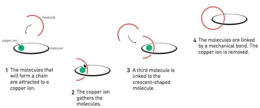
Jean-Pierre Sauvage used a copper ion to interlock molecules using a mechanical bond. (credit: The Royal Swedish Academy of Sciences)

The first step towards a molecular machine was taken by Jean-Pierre Sauvage in 1983, when he succeeded in linking two ring-shaped molecules together to form a chain, called a catenane. Normally, molecules are joined by strong covalent bonds in which the atoms share electrons, but in the chain they were instead linked by a freer mechanical bond. For a machine to be able to perform a task it must consist of parts that can move relative to each other. The two interlocked rings fulfilled exactly this requirement.

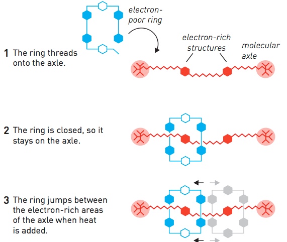
Fraser Stoddart created a rotaxane cyclophane ring that could act as a molecular shuttle, moving along an axle in a controlled manner. (credit: The Royal Swedish Academy of Sciences)

The second step was taken by Fraser Stoddart in 1991, when he developed a rotaxane. He threaded a rotaxane cyclophane molecular ring onto a thin molecular axle and demonstrated that the ring was able to move along the axle — the start of applying topological entanglement in the development of molecular machinery.

(Left) Fraser Stoddart’s (left) rotaxane-based “molecular elevator” and (right) “artificial muscle,” using extension and contraction in a daisy-chain rotaxane structure (credit: The Royal Swedish Academy of Sciences)

Among his other developments based on rotaxanes are a molecular lift, a molecular muscle and a molecule-based computer chip.

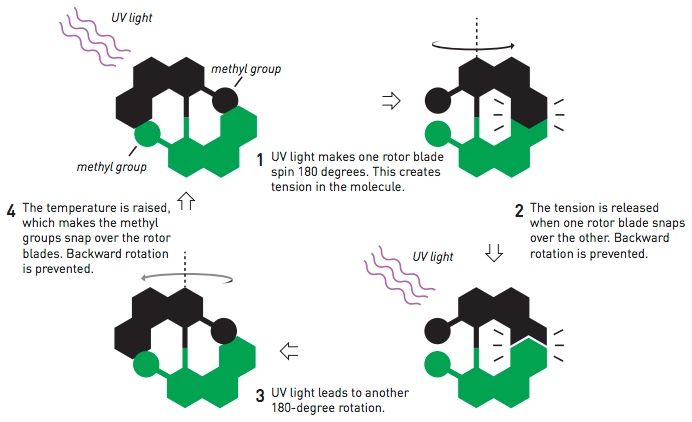
Ben Feringa’s molecular motor (the first) was mechanically constructed to spin in a particular direction. His research group has optimized the motor so that it now spins at 12 million revolutions per second. (credit: The Royal Swedish Academy of Sciences)

Bernard Feringa was the first person to develop a molecular motor; in 1999 he got a molecular rotor blade to spin continually in the same direction.

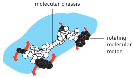
Ben Feringa’s four-wheel drive nanocar, with a molecular chassis and four motors that functioned as wheels (credit: The Royal Swedish Academy of Sciences)

Using molecular motors, he has also rotated a glass cylinder that is 10,000 times bigger than the motor and also designed a nanocar.

2016′s Nobel Laureates in Chemistry have taken molecular systems out of equilibrium’s stalemate and into energy-filled states in which their movements can be controlled. In terms of development, the molecular motor is at the same stage as the electric motor was in the 1830s, when scientists displayed various spinning cranks and wheels, unaware that they would lead to electric trains, washing machines, fans and food processors. Molecular machines will most likely be used in the development of things such as new materials, sensors and energy storage systems.

Jean-Pierre Sauvage, born 1944 in Paris, France. Ph.D. 1971 from the University of Strasbourg, France. Professor Emeritus at the University of Strasbourg and Director of Research Emeritus at the National Center for Scientific Research (CNRS), France.
https://isis.unistra.fr/laboratory-of-inorganic-chemistry-jean-pierre-sauvage

Sir J. Fraser Stoddart, born 1942 in Edinburgh, UK. Ph.D. 1966 from Edinburgh University, UK. Board of Trustees Professor of Chemistry at Northwestern University, Evanston, IL, USA.
http://stoddart.northwestern.edu

Bernard L. Feringa, born 1951 in Barger-Compascuum, the Netherlands. Ph.D.1978 from the University of Groningen, the Netherlands. Professor in Organic Chemistry at the University of Groningen, the Netherlands.
www.benferinga.com