Genetically engineered peptides on 2D nanosheets form bio-nano interfaces

A top view of GrBP5 nanowires on a 2-D surface of graphene (credit: Mehmet Sarikaya/Scientific Reports)

Engineers at the University of Washington have created genetically engineered peptides that self-assemble into arrays of nanowires on two-dimensional nanosheets (single-layer graphene and molybdenum disulfide) to relay information across a bio-nano interface — a first step towards fully self-assembled future biomedical and electro-optical bionanoelectronic devices.

Arrays of peptides could provide organized scaffolds for functional biomolecules, enabling nanoscale bioelectronics interfaces. And designed peptides could be incorporated with metal ions or nanoparticles with specific physical characteristics, thus fine-tuning 2D device performance for chemical and biological sensors.

A bridge between biology and technology

“Bridging this divide would be the key to building the genetically engineered biomolecular solid-state devices of the future,” said UW professor Mehmet Sarikaya in the Departments of Materials Science & Engineering, senior author of an open-access paper published Sept. 22 in Scientific Reports.

The UW team is also planning to develop genetically engineered peptides with specific chemical and structural properties. Their ideal peptide would change the physical properties of synthetic materials and respond to that change. That way, it would transmit “information” from the synthetic material to other biomolecules — bridging the chemical divide between biology and technology.

The peptides function through molecular recognition — the same principles that underlie biochemical interactions such as an antibody binding to its specific antigen or protein binding to DNA.
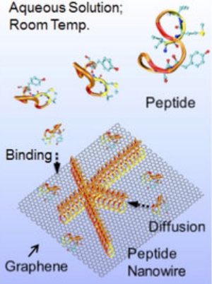
A schematic showing GrBP5 peptide self-organization with a series of surface processes on graphene: binding, diffusion and self-organization (credit: Yuhei Hayamizu et al./Scientific Reports)

In exploring the properties of 80 genetically selected peptides — which are not found in nature but have the same chemical components as peptides in all proteins — the researchers discovered that one peptide, GrBP5, showed promising interactions with the semimetal graphene. They tested GrBP5’s interactions with several other 2-D nanomaterials that “could serve as the metals or semiconductors of the future,” Sarikaya said.

Their experiments revealed that GrBP5 spontaneously organized into ordered nanowire patterns on graphene. With a few mutations, GrBP5 also altered the electrical conductivity of a graphene-based device, the first step toward transmitting electrical information from graphene to cells via peptides.

New bio-optoelectronic devices

Sarikaya’s team also modified GrBP5 to produce similar results on semiconductor material molybdenum disulfide (MoS2) and other materials* by converting a chemical signal to an optical signal. And they computationally predicted how different arrangements of GrBP5 nanowires would affect the electrical conduction or optical signal properties of each material.

A top view image of GrBP5 nanowires on a 2-D surface of molybdenum disulfide (credit: Mehmet Sarikaya/Scientific Reports)

The researchers are also seeking a peptide that could interact with materials such as gold, titanium, and even a mineral in bone and teeth.

Funded by the National Science Foundation, the UW, the National Institutes of Health, and the Japan Science and Technology Agency, the research is the focus of a new endeavor funded by the National Science Foundation’s Materials Genome Initiative. UW’s CoMotion is also working with Amazon to develop nano-sensors to detect early stages of pancreatic cancer.

* Other semiconducting 2D transition metal dichalcogenides (WSe2, WS2, MoSe2) along with insulating hBN, all with unique electronic and optical properties, were also tested.


Abstract of Bioelectronic interfaces by spontaneously organized peptides on 2D atomic single layer materials

Self-assembly of biological molecules on solid materials is central to the “bottom-up” approach to directly integrate biology with electronics. Inspired by biology, exquisite biomolecular nanoarchitectures have been formed on solid surfaces. We demonstrate that a combinatorially-selected dodecapeptide and its variants self-assemble into peptide nanowires on two-dimensional nanosheets, single-layer graphene and MoS2. The abrupt boundaries of nanowires create electronic junctions via spatial biomolecular doping of graphene and manifest themselves as a self-assembled electronic network. Furthermore, designed peptides form nanowires on single-layer MoS2 modifying both its electric conductivity and photoluminescence. The biomolecular doping of nanosheets defined by peptide nanostructures may represent the crucial first step in integrating biology with nano-electronics towards realizing fully self-assembled bionanoelectronic devices.

Graphene crowd-surfs on a lipid monolayer

Model of graphene on a lipid monolayer (credit: Universiteit Leiden)

“Crowd-surfing” on a smooth, supportive lipid monolayer, graphene could provide a versatile new platform for biosensors and drug delivery systems, researchers at Leiden University in The Netherlands have discovered.

Graphene is typically supported or sandwiched with other two-dimensional materials to promote higher mobility, ensure consistent electrical performance, and prevent environmental contamination. But combining graphene with soft, dynamic, molecular self-assembled lipid monolayers could provide a versatile platform for applications such as biosensors and drug delivery systems.

In research results published (open access) in a cover story in the journal Nanoscale on September 28, the authors note that the lipids (surprisingly) also improve graphene’s electrical conductivity. That could allow for measuring the electrical signals of graphene in the body for detecting acidity or the presence of certain proteins, for example.
This research was funded by the European Research Council, the Netherlands Organization for Scientific Research, and the Swiss National Science Foundation.

Abstract of Graphene-stabilized lipid monolayer heterostructures: a novel biomembrane superstructure

Chemically defined and electronically benign interfaces are attractive substrates for graphene and other two-dimensional materials. Here, we introduce lipid monolayers as an alternative, structurally ordered, and chemically versatile support for graphene. Deposition of graphene on the lipids resulted in a more ordered monolayer than regions without graphene. The lipids also offered graphene a more uniform and smoother support, reducing graphene hysteresis loop and the average value of the charge neutrality point under applied voltages. Our approach promises to be effective towards measuring experimentally biochemical phenomena within lipid monolayers and bilayers.

Self-powered ‘materials that compute’ and recognize simple patterns

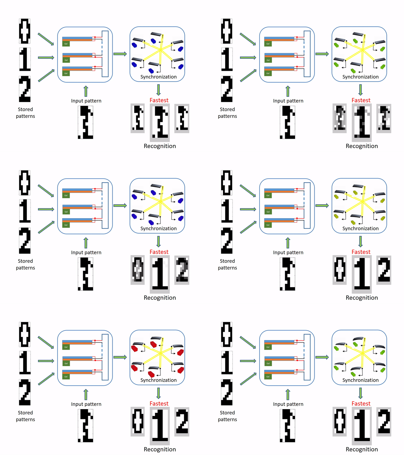
Conceptual illustration of pattern recognition process performed by hybrid gel-piezoelectric oscillator system (credit: Yan Fang)

University of Pittsburgh researchers have modeled the design of a “material that computes” — a hybrid material, powered only by its own chemical reactions, that can recognize simple patterns.

The material could one day be integrated into clothing and used to monitor the human body, or developed as a skin for “squishy” robots, for example, according to the researchers, writing in the open-access AAAS journal Science Advances.

A computer that combines gels and piezeoelectric materials

The computations (needed to design the hypothetical material) were modeled utilizing Belousov-Zhabotinsky (BZ) gels, a substance that oscillates in the absence of external stimuli, combined with an overlaying piezoelectric (PZ) cantilever, forming “BZ-PZ” (as in “easy peasy”). The BZ gels oscillate periodically, triggered by chemical stimulation, without the need for external driving stimuli. Piezoelectric (PZ) materials generate a voltage when deformed and, conversely, undergo deformation in the presence of an applied voltage.

Two BZ-PZ oscillator units connected with electrical wires. Triggered by the chemical oscillations, the BZ gels (green) expand in volume, generating a force (F1 and F2) and thereby cause the deflections ξ1 and ξ2 of the PZ cantilevers (orange and blue layers) , which generate an electric voltage U. That voltage then deflects the cantilevers (the inverse PZ effect), which then compress the underlying BZ gels and thereby modify the chemomechanical oscillations in these gels. The end result is the components’ response to self-generated signals (sensing), volumetric changes in the gel (actuation), and the passage of signals between the units (communication). For computation, the communication also leads to synchronization of the BZ gel oscillators. (credit: Yan Fang et al./Science Advances)

“By combining these attributes into a ‘BZ-PZ’ unit and then connecting the units by electrical wires, we designed a device that senses, actuates, and communicates without an external electrical power source,” the researchers explain in the paper.*

The result is that the device can also be used to perform computation. To use that for pattern recognition, the researchers first stored a pattern of numbers as a set of polarities in the BZ-PZ units, and the input patterns were coded with the initial phase of the oscillations imposed on these units.

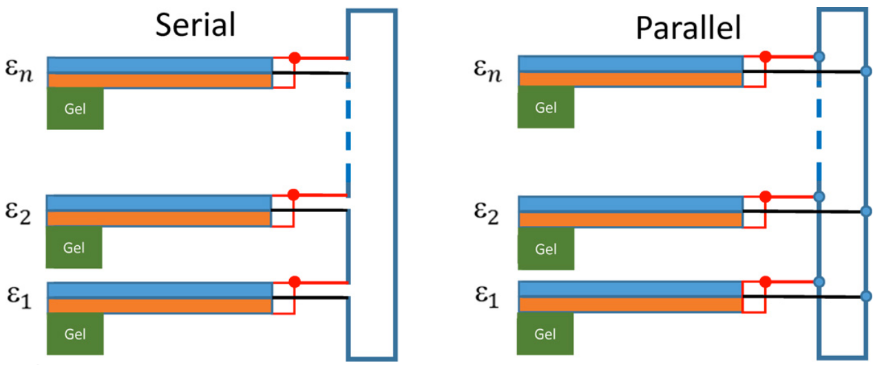
Multiple BZ-PS units wired in serial and parallel configurations to form a network (credit: Yan Fang et al./Science Advances)

With multiple BZ-PZ units, the oscillators can be wired into a network  formed, for example, from units that are connected in parallel or in series. The resulting transduction between chemomechanical and electrical energy creates signals that quickly propagate and thus permits remote coupled oscillators to communicate and synchronize. This synchronization behavior in BZ-PZ network can be used for oscillator-based computing.

The computational modeling revealed that the input pattern closest to the stored pattern exhibits the fastest convergence time to the stable synchronization behavior, and is the most effective at recognizing patterns. In this study, the materials were programmed to recognize black-and-white pixels in the shape of numbers that had been distorted.

The researchers’ next goal is to expand from analyzing black-and-white pixels to grayscale and more complicated images and shapes, as well as to enhance the devices storage capability.

Perfect for monitoring human and robot bodies

Compared to a traditional computer, these computations are slow and take minutes. “Individual events are slow because the period of the BZ oscillations is slow,” said Victor V. Yashin, Research Assistant Professor of Chemical and Petroleum Engineering. “However, there are some tasks that need a longer analysis, and are more natural in function. That’s why this type of system is perfect to monitor environments like the human body.”

For example, Dr. Yashin said that patients recovering from a hand injury could wear a glove that monitors movement, and can inform doctors whether the hand is healing properly or if the patient has improved mobility. Another use would be to monitor individuals at risk for early onset Alzheimer’s, by wearing footwear that would analyze gait and compare results against normal movements, or a garment that monitors cardiovascular activity for people at risk of heart disease or stroke.

Since the devices convert chemical reactions to electrical energy, there would be no need for external electrical power. This would also be ideal for a robot or other device that could utilize the material as a sensory skin.

The research is funded by a five-year National Science Foundation Integrated NSF Support Promoting Interdisciplinary Research and Education (INSPIRE) grant, which focuses on complex and pressing scientific problems that lie at the intersection of traditional disciplines.

“This work at the University of Pittsburgh … is an example of this groundbreaking shift away from traditional silicon CMOS-based digital computing to a non-von Neumann machine in a polymer substrate, with remarkable low power consumption,” said Sankar Basu, NSF program director.

* This continues the research of Anna C. Balazs, Distinguished Professor of Chemical and Petroleum Engineering, and Steven P. Levitan, the John A. Jurenko Professor of Electrical and Computer Engineering. 


Abstract of Pattern recognition with “materials that compute”

Driven by advances in materials and computer science, researchers are attempting to design systems where the computer and material are one and the same entity. Using theoretical and computational modeling, we design a hybrid material system that can autonomously transduce chemical, mechanical, and electrical energy to perform a computational task in a self-organized manner, without the need for external electrical power sources. Each unit in this system integrates a self-oscillating gel, which undergoes the Belousov-Zhabotinsky (BZ) reaction, with an overlaying piezoelectric (PZ) cantilever. The chemomechanical oscillations of the BZ gels deflect the PZ layer, which consequently generates a voltage across the material. When these BZ-PZ units are connected in series by electrical wires, the oscillations of these units become synchronized across the network, where the mode of synchronization depends on the polarity of the PZ. We show that the network of coupled, synchronizing BZ-PZ oscillators can perform pattern recognition. The “stored” patterns are set of polarities of the individual BZ-PZ units, and the “input” patterns are coded through the initial phase of the oscillations imposed on these units. The results of the modeling show that the input pattern closest to the stored pattern exhibits the fastest convergence time to stable synchronization behavior. In this way, networks of coupled BZ-PZ oscillators achieve pattern recognition. Further, we show that the convergence time to stable synchronization provides a robust measure of the degree of match between the input and stored patterns. Through these studies, we establish experimentally realizable design rules for creating “materials that compute.”

‘Perfect’ low-cost, defect-free graphene directly from graphite

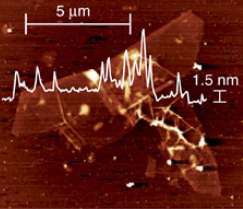
Atomic force microscope (AFM) image with height profile indicating the single-layer nature of the obtained graphene, with lateral dimensions of ~10 micrometers and a height of ~1.5 nanometers. (credit: Philipp Vecera et al./Nature Communications)

Chemists at the University of Erlangen-Nürnberg (FAU) in Germany and the University of Vienna have succeeded in producing “perfect” defect-free, high-quality graphene directly from graphite (“pencil lead”) for the first time. This new low-cost method may make it possible for the semiconductor industry to scale up use of graphene in pioneering technologies such as transparent electrodes for flexible displays.

The chemists say their method enables the graphene to be cut without causing defects and allows specific electronic properties to be set. That makes this new scalable, inexpensive method for graphene production a significant improvement over previous wet-chemical approaches, which have size limitations and excessive defects, lowering the conductivity .

Graphene is usually processed using chemical exfoliation (peeling off) of graphite. In this process, metal ions are embedded in graphite, resulting in an intercalated (layered) compound. The individual layers of carbon are separated using solvents. The stabilized graphene then has to be separated from the solvent and reoxidised. However, defects in the individual layers of carbon, such as hydration and oxidation of carbon atoms in the lattice, can occur during this process.

FAU researchers have now found a solution to this problem: adding the solvent benzonitrile, which allows the defect-free graphene to be removed without any additional functional groups forming.

In addition, the benzonitrile (PhCN) molecule formed during the reduction reaction turns red. This change in color allows the number of charge carriers in the system to be determined easily through absorption measurements instead of requiring complex voltage measurements.

The researchers published their findings August 10 in the open-access journal Nature Communications.


Abstract of Solvent-driven electron trapping and mass transport in reduced graphites to access perfect graphene

Herein, we report on a significant discovery, namely, the quantitative discharging of reduced graphite forms, such as graphite intercalation compounds, graphenide dispersions and graphenides deposited on surfaces with the simple solvent benzonitrile. Because of its comparatively low reduction potential, benzonitrile is reduced during this process to the radical anion, which exhibits a red colour and serves as a reporter molecule for the quantitative determination of negative charges on the carbon sheets. Moreover, this discovery reveals a very fundamental physical–chemical phenomenon, namely a quantitative solvent reduction induced and electrostatically driven mass transport of K+ ions from the graphite intercalation compounds into the liquid. The simple treatment of dispersed graphenides suspended on silica substrates with benzonitrile leads to the clean conversion to graphene. This unprecedented procedure represents a rather mild, scalable and inexpensive method for graphene production surpassing previous wet-chemical approaches.

3-D-printed structures that ‘remember’ their shapes

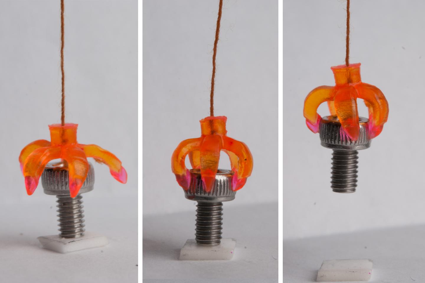
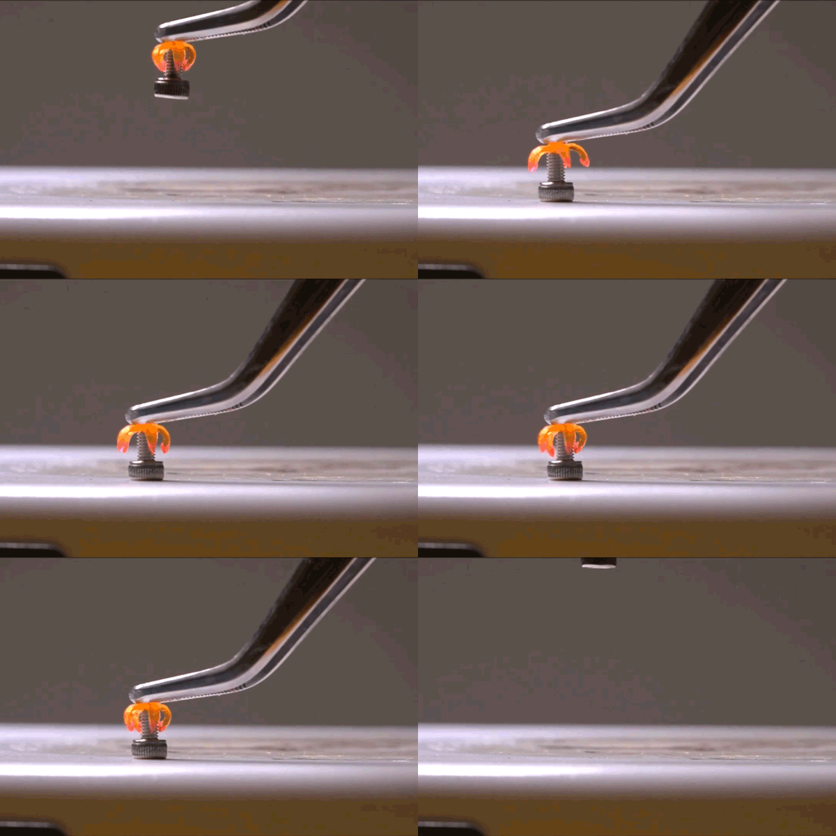
In this series, a 3-D printed multimaterial shape-memory minigripper, consisting of shape-memory hinges and adaptive touching tips, grasps a cap screw. The material is designed to close when the temperature of the surrounding air is raised to specific temperature or higher (credit: Qi (Kevin) Ge)

Engineers from MIT and Singapore University of Technology and Design (SUTD) are 3D-printing structures based on shape-memory polymers that “remember” and spring back to their original shapes when heated to a certain temperature “sweet spot” — even after being stretched, twisted, and bent at extreme angles.

That makes them useful for applications ranging from soft actuators that turn solar panels toward the sun to tiny drug capsules that open upon early signs of infection. Other applications include biomedical devices, deployable aerospace structures, and shape-changing photovoltaic solar cells.

For some structures, the researchers were able to 3D-print micrometer-scale features as small as the diameter of a human hair — dimensions at least ten times smaller than with other printable shape-memory materials, but with materials that can be stretched 10 times larger than those printed by commercial 3-D printers.

The team’s results were published earlier this month in the online open-access journal Scientific Reports.

“We ultimately want to use body temperature as a trigger,” says Nicholas X. Fang, associate professor of mechanical engineering at MIT. “If we can design these polymers properly, we may be able to form a drug delivery device that will only release medicine at the sign of a fever.”

”Fang and others have been exploring the use of soft, active materials as reliable, pliable tools. These new and emerging materials, which include shape-memory polymers, can stretch and deform dramatically in response to environmental stimuli such as heat, light, and electricity — properties that researchers have been investigating for use in biomedical devices, soft robotics, wearable sensors, and artificial muscles.

Shape-memory polymers can switch between two states — a harder, low-temperature, amorphous state, and a soft, high-temperature, rubbery state. The bent and stretched shapes can be “frozen” at room temperature, and when heated the materials will “remember” and snap back to their original sturdy form.

“If you’re able to make it to much smaller dimensions, these materials can actually respond very quickly, within seconds,” Fang says. “For example, a flower can release pollen in milliseconds. It can only do that because its actuation mechanisms are at the micron scale.”

Printing with light

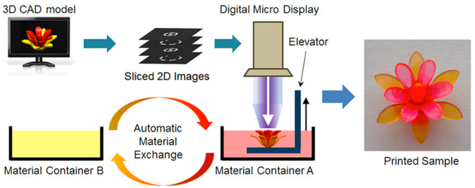
Workflow for the process of fabricating a multimaterial structure based on microstereolithography (credit: Qi Ge et al./Scientific Reports)

To print shape-memory structures with even finer details, Fang and his colleagues used a 3-D printing process they have pioneered, called “microstereolithography” (PμSL), in which they use light from a projector to print patterns on successive layers of resin. It uses a family of photo-curable methacrylate-based copolymer networks, designing the constituents and compositions to exhibit desired thermomechanical behavior.*

The researchers first create a model of a structure using computer-aided design (CAD) software, then divide the model into hundreds of slices, each of which they send through the projector as a bitmap — an image file format that represents each layer as an arrangement of very fine pixels. The projector then shines light in the pattern of the bitmap, onto a liquid resin, or polymer solution, etching the pattern into the resin, which then solidifies.

Fang found that the structures could be stretched to three times their original length without breaking. “Because we’re using our own printers that offer much smaller pixel size, we’re seeing much faster response, on the order of seconds,” Fang says. “If we can push to even smaller dimensions, we may also be able to push their response time, to milliseconds.”

“This is a very advanced 3-D printing method compared to traditional nozzle or ink-jet based printers,” says Shaochen Chen, professor of nano-engineering at the University of California at San Diego, who was not involved in the research. “The method’s main advantages are faster printing and better structural integrity.”

Soft grip

To demonstrate a simple application for the shape-memory structures, Fang and his colleagues printed a small, rubbery, claw-like gripper. They attached a thin handle to the base of the gripper, then stretched the gripper’s claws open.

“The grippers are a nice example of how manipulation can be done with soft materials,” Fang says. “We showed that it is possible to pick up a small bolt, and also even fish eggs and soft tofu. That type of soft grip is probably very unique and beneficial.”

Going forward, he hopes to find combinations of polymers to make shape-memory materials that react to slightly lower temperatures, approaching the range of human body temperatures, to design soft, active, controllable drug delivery capsules. He says the material may also be printed as soft, responsive hinges to help solar panels track the sun.

Scientists at Rutgers University, SUTD, and Georgia Institute of Technology were also involved in the research, which is supported in part by the SUTD Digital Manufacturing and Design Center (DManD) and the SUTD-MIT joint postdoctoral program.

* “We’re printing with light, layer by layer,” Fang says. “It’s almost like how dentists form replicas of teeth and fill cavities, except that we’re doing it with high-resolution lenses that come from the semiconductor industry, which give us intricate parts, with dimensions comparable to the diameter of a human hair.”

The researchers looked through the scientific literature to identify an ideal mix of polymers to create a shape-memory material on which to print their light patterns. They picked two polymers, one composed of long-chain polymers, or spaghetti-like strands, and the other resembling more of a stiff scaffold. When mixed together and cured, the material can be stretched and twisted dramatically without breaking.

What’s more, the material can bounce back to its original printed form, within a specific temperature range — in this case, between 40 and 180 degrees Celsius (104 to 356 degrees Fahrenheit).


Abstract of Multimaterial 4D Printing with Tailorable Shape Memory Polymers

We present a new 4D printing approach that can create high resolution (up to a few microns), multimaterial shape memory polymer (SMP) architectures. The approach is based on high resolution projection microstereolithography (PμSL) and uses a family of photo-curable methacrylate based copolymer networks. We designed the constituents and compositions to exhibit desired thermomechanical behavior (including rubbery modulus, glass transition temperature and failure strain which is more than 300% and larger than any existing printable materials) to enable controlled shape memory behavior. We used a high resolution, high contrast digital micro display to ensure high resolution of photo-curing methacrylate based SMPs that requires higher exposure energy than more common acrylate based polymers. An automated material exchange process enables the manufacture of 3D composite architectures from multiple photo-curable SMPs. In order to understand the behavior of the 3D composite microarchitectures, we carry out high fidelity computational simulations of their complex nonlinear, time-dependent behavior and study important design considerations including local deformation, shape fixity and free recovery rate. Simulations are in good agreement with experiments for a series of single and multimaterial components and can be used to facilitate the design of SMP 3D structures.

The first autonomous soft robot powered only by a chemical reaction

Harvard’s “octobot” is powered by a chemical reaction and controlled with a soft logic board. A reaction inside the bot transforms a small amount of liquid fuel (hydrogen peroxide) into a large amount of oxygen gas, which flows into the octobot’s arms and inflates them like a balloon. The team used a microfluidic logic circuit, a soft analogue of a simple electronic oscillator, to control when hydrogen peroxide decomposes to gas in the octobot. Octopi have long been a source of inspiration in soft robotics. These curious creatures can perform incredible feats of strength and dexterity with no internal skeleton. (SD card shown for scale only.) (credit: Lori Sanders)

The first autonomous, untethered, entirely soft 3-D-printed robot (powered only by a chemical reaction) has been demonstrated by a team of Harvard University researchers and described in the journal Nature.

Nicknamed “octobot,” the bot combines soft lithography, molding, and 3-D printing.

“One longstanding vision for the field of soft robotics has been to create robots that are entirely soft, but the struggle has always been in replacing rigid components like batteries and electronic controls with analogous soft systems and then putting it all together,” said Harvard professor Robert Wood. “This research demonstrates that we can easily manufacture the key components of a simple, entirely soft robot, which lays the foundation for more complex designs.”

Powered by hydrogen peroxide

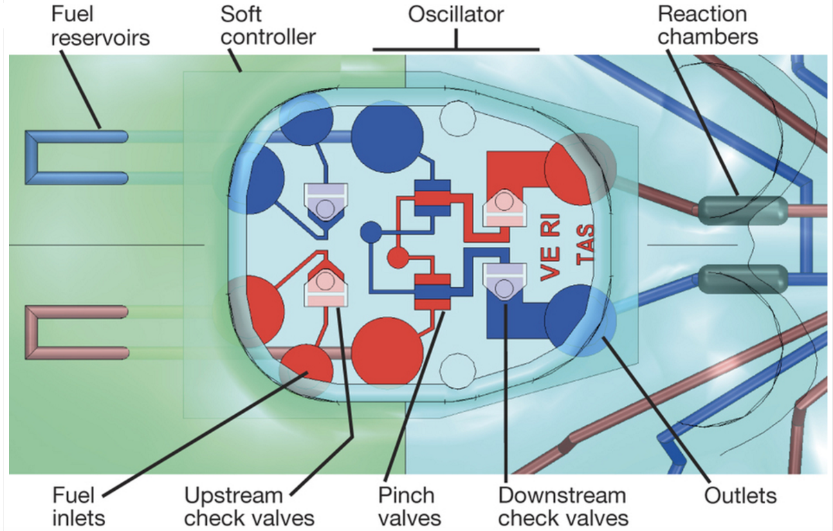
Octobot structure. A system of check valves and switch valves within the soft controller regulates fluid flow into and through the system. The reaction chambers convert the hydrogen peroxide to oxygen, which then inflates the bot arms. The 500-micrometers-high “VERITAS” letters are patterned into the soft controller as an indication of scale. (credit: Michael Wehner et al./Nature)

Harvard’s octobot is pneumatic-based — powered by gas under pressure. A reaction inside the bot transforms a small amount of liquid fuel (hydrogen peroxide) into a large amount of gas, which flows into the octobot’s arms and inflates them like balloons. To control the reaction, the team used a microfluidic logic circuit based on pioneering work by co-author and chemist George Whitesides.

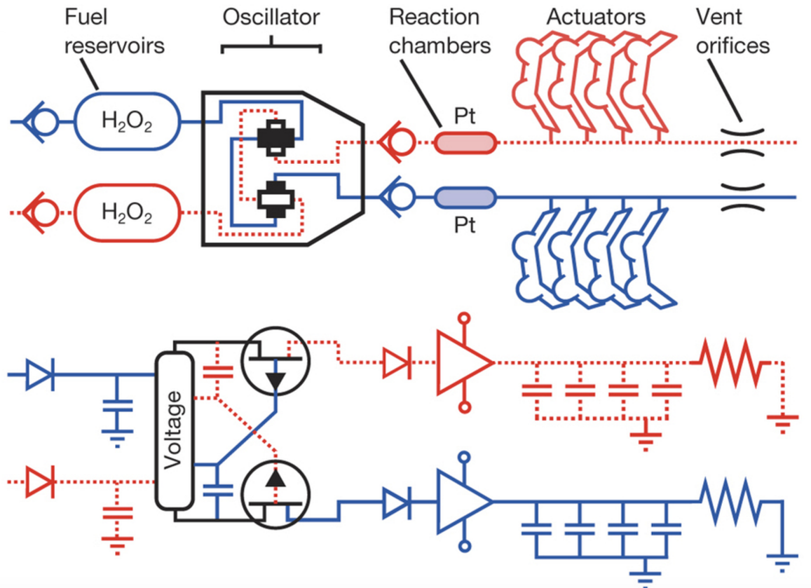
Octobot mechanical schematic (top) and electronic analogue (bottom). Check valves, fuel tanks, oscillator, reaction chambers, actuators and vent orifices are analogous to diodes, supply capacitors, electrical oscillator, amplifiers, capacitors and pull-down resistors, respectively. (credit: Michael Wehner at al./Nature)

The circuit, a soft analogue of a simple electronic oscillator, controls when hydrogen peroxide decomposes to gas in the octobot, triggering actuators.

The proof-of-concept octobot design could pave the way for a new generation of such machines, which could help revolutionize how humans interact with machines, the researchers suggest. They hope their approach for creating autonomous soft robots inspires roboticists, material scientists, and researchers focused on advanced manufacturing.

Next, the Harvard team hopes to design an octobot that can crawl, swim, and interact with its environment.

Robert Wood, the Charles River Professor of Engineering and Applied Sciences, and Jennifer A. Lewis, the Hansjorg Wyss Professor of Biologically Inspired Engineering, at the Harvard John A. Paulson School of Engineering and Applied Sciences (SEAS), led the research. Lewis and Wood are also core faculty members of the Wyss Institute for Biologically Inspired Engineering at Harvard University. George Whitesides is the Woodford L. and Ann A. Flowers University Professor and a core faculty member of the Wyss.

The research was supported by the National Science Foundation through the Materials Research Science and Engineering Center at Harvard and by the Wyss Institute.


Harvard University | Introducing the Octobot


Harvard University | Powering the Octobot: A chemical reaction


Abstract of An integrated design and fabrication strategy for entirely soft, autonomous robots

Soft robots possess many attributes that are difficult, if not impossible, to achieve with conventional robots composed of rigid materials. Yet, despite recent advances, soft robots must still be tethered to hard robotic control systems and power sources. New strategies for creating completely soft robots, including soft analogues of these crucial components, are needed to realize their full potential. Here we report the untethered operation of a robot composed solely of soft materials. The robot is controlled with microfluidic logic that autonomously regulates fluid flow and, hence, catalytic decomposition of an on-board monopropellant fuel supply. Gas generated from the fuel decomposition inflates fluidic networks downstream of the reaction sites, resulting in actuation. The body and microfluidic logic of the robot are fabricated using moulding and soft lithography, respectively, and the pneumatic actuator networks, on-board fuel reservoirs and catalytic reaction chambers needed for movement are patterned within the body via a multi-material, embedded 3D printing technique. The fluidic and elastomeric architectures required for function span several orders of magnitude from the microscale to the macroscale. Our integrated design and rapid fabrication approach enables the programmable assembly of multiple materials within this architecture, laying the foundation for completely soft, autonomous robots.

How to separate out semiconducting carbon nanotubes

Artistic rendition of a metallic carbon nanotube being pulled into solution, in analogy to the work described by the Adronov group (credit: Alex Adronov, McMaster University)

Researchers at McMaster University in Canada have developed a radically improved way to purify single-wall carbon nanotubes (SWNTs) — flexible structures that are one nanometer in diameter and thousands of times longer, ­and that may revolutionize computers and electronics, replacing silicon.

To do that, we need to separate out semiconducting (sc-SWNTs) and metallic (m-SWNTs) nanotubes. That’s a challenging problem, because both are created simultaneously in the process* of producing carbon nanotubes.

“Once we have a reliable source of pure nanotubes that are not very expensive, a lot can happen very quickly,” says Alex Adronov, a professor of Chemistry at McMaster whose research team has developed a new and potentially cost-efficient way to purify carbon nanotubes.

Separating out semiconducting carbon nanotubes

Previous researchers have created polymers that could allow semiconducting carbon nanotubes to be dissolved and washed away, leaving metallic nanotubes behind, but there has not been such a process for doing the more-useful opposite: dispersing the metallic nanotubes and leaving behind the valuable semiconducting structures.

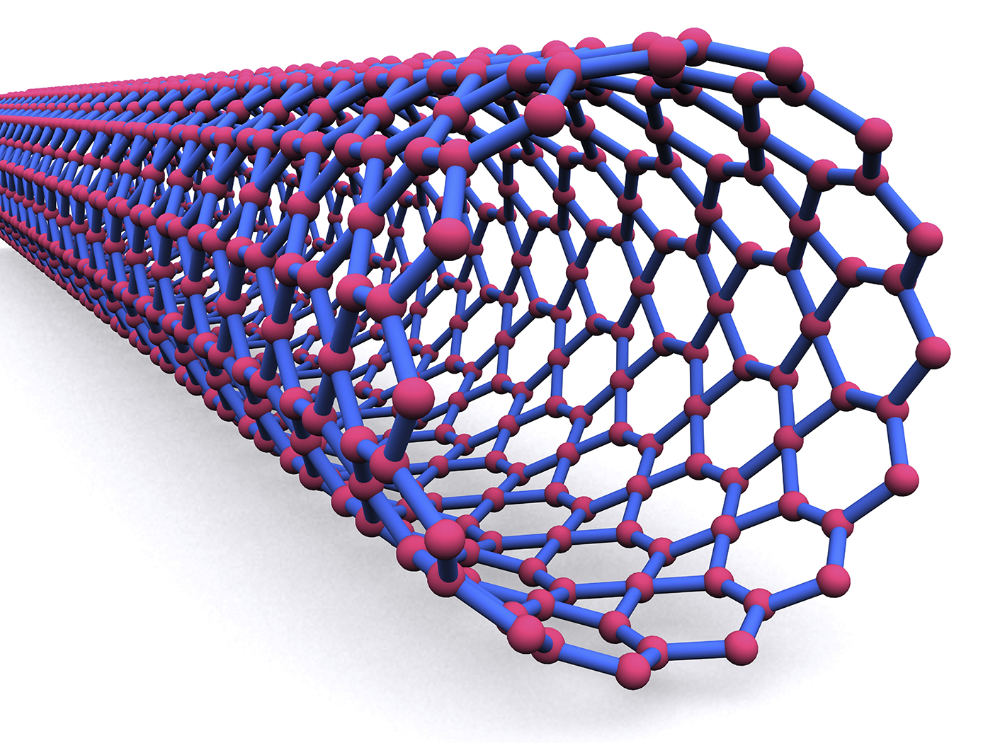
Single-wall carbon nanotube (credit: NASA)

Now, Adronov’s research group has reversed the electronic characteristics (from electron-rich to electron-poor) of a polymer known to disperse semiconducting nanotubes, while leaving the rest of the polymer’s structure intact. That is, they have reversed the purification process — leaving the semiconducting nanotubes behind while making it possible to disperse the metallic nanotubes.**

The next step, he explains, is for his team or other researchers to exploit the discovery by finding a way to develop even more efficient polymers and scale up the process for commercial production.

The unique properties of SWNTs — high ten­sile strength, the high aspect ratio, thermal and electrical conductivity, and extraordinary optical characteristics — could make carbon nanotubes potentially valuable as advanced materials in a variety of applications, including “field-effect transistors, photovoltaics, flexible electronics, sensors, touch screens, high-strength fibers, biotech­nological constructs, and various other devices,” the researchers note in the current cover story of Chemistry – A European Journal.

Financial support for this work was provided by the Discovery and Strategic Grant programs of the Natural Science and Engi­neering Research Council (NSERC) of Canada.

* These processes include high-pressure carbon monoxide disproportionation (HiPCO),carbon vapor deposition (CVD),arc discharge,laser ablation, and plasma torch growth.

** “We expect that relatively electron-poor con­jugated polymers should disperse m-SWNTs to a greater extent when compared to structurally similar electron-rich conjugated polymers. Here, we demonstrate this concept through the comparison of a poly(fluorene-co-pyridine) conjugated polymer before and after post-polymerization functionalization. By par­tially methylating the pyridine units, cationic charges are intro­duced onto the conjugated backbone, which convert the polymer from being electron-rich to electron-poor. This enables the comparison of two polymers that are identical in length and polydispersity, and differ primarily in their electronic character­istics. We show that the electron-poor conjugated polymer re­sults in dispersions that are enriched in m-SWNTs, while the electron-rich counterpart solely selects for sc-SWNTs, thus pro­viding evidence that the electronic structure of a conjugated polymer plays an important role in determining its selectivity for different SWNT types.” — Darryl Fong et al./Chemistry – A European Journal.


Abstract of Influence of Polymer Electronics on Selective Dispersion of Single-Walled Carbon Nanotubes

In the pursuit of next-generation polymers for the selective dispersion and purification of single-walled carbon nanotubes (SWNTs), understanding the key parameters dictating polymer selectivity is imperative. Simple modification of a poly(fluorene-co-pyridine) backbone, such that it is transformed from being electron-rich to -poor, has a significant impact on the electronic nature of the SWNTs dispersed. The unmodified copolymer bearing an electron-rich fluorene co-monomer preferentially forms stable colloids with sc-SWNTs, while the methylated copolymer bearing electron-withdrawing cationic charges produces dispersions that are more enriched with m-SWNTs.

New cancer-drug delivery system uses magnetically guided bacteria to target cancerous tumors with high precision

Artist’s impression of new cancer-drug nanotransporters using more than 100 million self-propelled, flagellated bacteria carrying nanoliposomes (green discs) loaded with drugs. The bacteria are guided by magnetic fields to take the most direct path between the drug’s injection point and the area of the body intended to cure. (credit: Montréal Nanorobotics Laboratory)

Researchers from Polytechnique Montréal, Université de Montréal, and McGill University have designed a new cancer-drug-delivery nanotransporter system using more than 100 million flagellated, self-propelled bacteria that are capable of navigating through the bloodstream to administer a drug to tumors with precision.* The goal of the research is to avoid jeopardizing the integrity of organs and surrounding healthy tissues while reducing drug dosage.

In an experiment with mice reported in the journal Nature Nanotechnology, the researchers confirmed that “the drug’s propelling force was enough to travel efficiently and enter deep inside the tumors,” autonomously detecting the oxygen-depleted tumor areas and delivering the drug to them, said Professor Sylvain Martel, holder of the Canada Research Chair in Medical Nanorobotics and Director of the Polytechnique Montréal Nanorobotics Laboratory, who heads the research team’s work.

Bacteria that detect both magnetic field lines and low-oxygen concentrations

In the experiment with mice, the researchers used liposomes as drug nanocarriers, attached to Magnetococcus marinus strain MC-1 bacteria to transport the drug**. In their natural environment, MC-1 bacteria tend to swim along local magnetic field lines, which are detected by a chain of magnetic iron-oxide nanocrystals in the bacteria. The bacteria also swim towards hypoxic (low-oxygen) concentrations. (In a tumor, this hypoxic zone is created by the substantial consumption of oxygen by rapidly proliferative tumor cells. Hypoxic zones are known to be resistant to most therapies, including radiotherapy.)

Test of penetration of live MC-1 bacteria cells with and without magnetic field exposure in xenografts following a peritumoral injection. (left) Magnetotaxis directional control system used to generate the magnetic field necessary to guide the MC-1 cells towards the xenograft. The directional magnetic field B was aligned towards the center of the tumoral volume. (center) MC-1 peritumoral injection into tumor xenograft in mice and representation of the applied directional magnetic field used in this study to direct the bacteria towards the xenograft. (right) Summary of the total average numbers of injected and detected MC-1 cells for all tumors in groups I and II. The results show that a significant number of the peritumorally injected MC-1 cells that were magnetically guided — using a relatively simple static directional magnetic field — were able to penetrate the xenograft, unlike the case for bacteria that were not guided into the tumor. (credit: Ouajdi Felfoul et al./Nature Nanotechnology)

The new nanotransporters used both of these natural systems (magnetic and hypoxic-concentration-seeking). The MC-1 bacteria first moved in the direction of a computer-controlled magnetic field to the point where oxygen gradients could be detected by the bacteria, enabling the bacteria to penetrate and remain in the tumor’s active regions. (In future human use, the drug could be released from the liposomes by sensing pH or particular enzymes, or by applying ultrasonics or heat, for example, the researchers explained to KurzweilAI.)

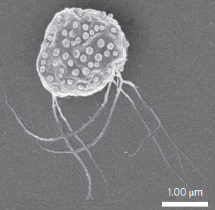
Scanning electron microscopy image of MC-1 bacterium with ~70 drug-bearing liposomes attached to the surface (credit: Ouajdi Felfoul et al./Nature Nanotechnology)

“This innovative use of nanotransporters will have an impact not only on creating more advanced engineering concepts and original intervention methods, but it also throws the door wide open to the synthesis of new vehicles for therapeutic, imaging, and diagnostic agents,” said Martel. Chemotherapy, which is so toxic for the entire human body, could make use of these natural nanotransporters to move drugs directly to the targeted area, “eliminating the harmful side effects while also boosting its therapeutic effectiveness,” he added.

The research was supported by the Consortium québécois sur la découverte du médicament (Québec consortium for drug discovery — CQDM), the Canada Research Chairs, the Natural Sciences and Engineering Research Council of Canada (NSERC), the Research Chair in Nanorobotics of Polytechnique Montréal, Mitacs, the Canada Foundation for Innovation (CFI), and the National Institutes of Health (NIH). Montréal’s Jewish General Hospital, the McGill University Health Centre (MUHC), the Institute for Research in Immunology and Cancer (IRIC), and the Rosalind and Morris Goodman Cancer Research Centre also participated.

* Only ∼2% of the total administered dose is deposited in the tumor with current delivery methods, according to a 2009 study by M. Hong et al. in J. Control. Rel., the researchers note in their Nature Nanotechnology paper.

** “Liposomes were selected as a first proof of concept because they are biocompatible, exhibit low immunogenicity and high flexibility, and protect the body from potential toxic cargo. Liposomes also shield therapeutic agents from premature degradation, control release kinetics, and may encapsulate a multitude of hydrophilic and∕or hydrophobic drug cargos, pharmaceutical ingredients, imaging agents and genetic material by virtue of their aqueous interior and lipid exterior,” the researchers note in their Nature Nanotechnology paper.


POLYTECHNIQUE MONTRÉAL | A Robotic Micro-assembly Process Inspired by the Construction of the Ancient Pyramids and Relying on Several Thousand of Flagellated Bacteria Acting as Workers


Abstract of Magneto-aerotactic bacteria deliver drug-containing nanoliposomes to tumour hypoxic regions

Oxygen-depleted hypoxic regions in the tumour are generally resistant to therapies. Although nanocarriers have been used to deliver drugs, the targeting ratios have been very low. Here, we show that the magneto-aerotactic migration behaviour of magnetotactic bacteria, Magnetococcus marinus strain MC-1, can be used to transport drug-loaded nanoliposomes into hypoxic regions of the tumour. In their natural environment, MC-1 cells, each containing a chain of magnetic iron-oxide nanocrystals, tend to swim along local magnetic field lines and towards low oxygen concentrationsbased on a two-state aerotactic sensing system. We show that when MC-1 cells bearing covalently bound drug-containing nanoliposomes were injected near the tumour in severe combined immunodeficient beige mice and magnetically guided, up to 55% of MC-1 cells penetrated into hypoxic regions of HCT116 colorectal xenografts. Approximately 70 drug-loaded nanoliposomes were attached to each MC-1 cell. Our results suggest that harnessing swarms of microorganisms exhibiting magneto-aerotactic behaviour can significantly improve the therapeutic index of various nanocarriers in tumour hypoxic regions.

Seeing the invisible: visible-light metamaterial superlens made from nanobeads

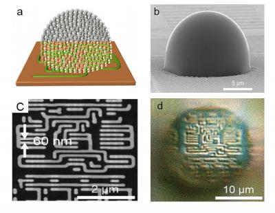
(a) Conceptual drawing of nanoparticle-based metamaterial solid immersion lens (mSIL) (b) Lab-made mSIL using titanium dioxide nanoparticles (c) SEM image of 60 nm size imaging sample (d) corresponding superlens imaging of the 60 nm sample by the developed mSIL. (credit: BangorUniversity/Fudan University)

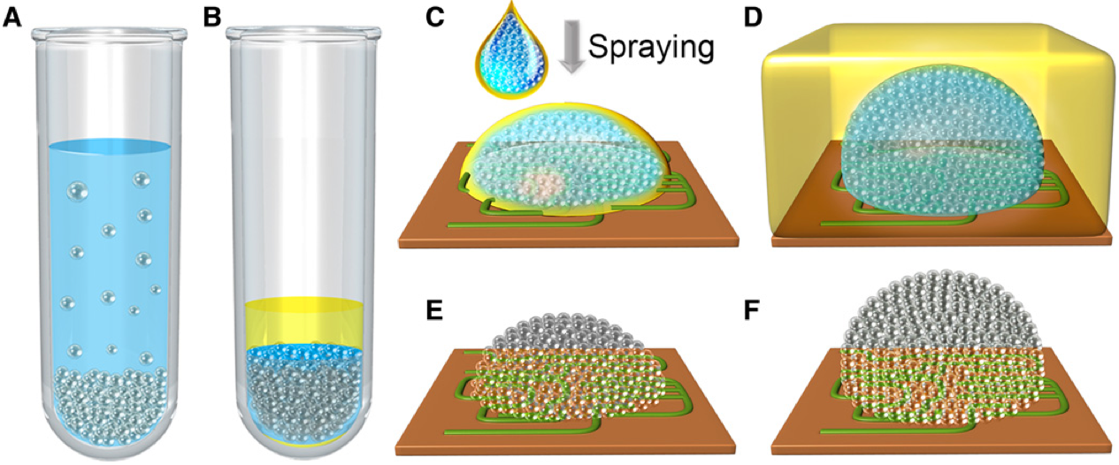
A team of British and Chinese scientists has developed a new “metamaterial-based solid immersion lens” (mSIL) microscope lens design that can extend the magnification of an optical microscope to see objects smaller than the approximately 200 nanometers Abbe diffraction limit, the smallest size of bacteria.

Led by Zengbo Wang, PhD, at Bangor University UK and Prof Limin Wu at Fudan University, China, the team created minute droplet-like lens structures on the surface to be examined. These act as an additional lens to magnify the surface features previously invisible to a normal microscope lens, adding 5x magnification to existing microscopes.

Schematic illustration of the assembly of the all-dielectric TiO2 mSIL. (A) Anatase TiO2 nanoparticles (15 nm) were centrifuged into a tightly packed precipitate. (B) The supernatant was replaced by an organic solvent mixture consisting of hexane and tetrachloroethylene to form a TiO2 nano–solid-fluid. (C) To prepare a hemispherical mSIL, the nano–solid-fluid was directly sprayed onto the sample surface. (D) To prepare a super-hemispherical mSIL, the nano–solid-fluid was sprayed onto the sample surface covered by a thin layer of organic solvent mixture. (E and F) After evaporation of the solvents, the nanoparticles underwent a phase transition to form a more densely packed structure. (credit: Wen Fan et al./Science Advances)

Made of millions of nanobeads, the spheres break up the light beam. Acting as individual minute beams, each bead refracts the light. “We’ve used high-index titanium dioxide (TiO2) nanoparticles as the building element of the lens,” Wang says. “These nanoparticles are able to bend light to a higher degree than water.”

“Each sphere bends the light to a high magnitude and splits the light beam, creating millions of individual beams of light. It is these tiny light beams which enable us to view previously unseen detail.”

Wang believes that the results will be easily replicable and that other labs will soon be adopting the technology and using it for themselves. Titanium dioxide is cheap and readily available, so rather than buying a new microscope, the lenses are applied to the material to be viewed, rather than to the microscope.

“The next challenge is to adapt the technology for use in biology and medicine. This would not require the current use of a combination of dyes and stains and laser light, which change the samples being viewed,” he says.

The lens is described in a paper in the open-access journal Science Advances today (August 12).


Abstract of Three-dimensional all-dielectric metamaterial solid immersion lens for subwavelength imaging at visible frequencies

Although all-dielectric metamaterials offer a low-loss alternative to current metal-based metamaterials to manipulate light at the nanoscale and may have important applications, very few have been reported to date owing to the current nanofabrication technologies. We develop a new “nano–solid-fluid assembly” method using 15-nm TiO2 nanoparticles as building blocks to fabricate the first three-dimensional (3D) all-dielectric metamaterial at visible frequencies. Because of its optical transparency, high refractive index, and deep-subwavelength structures, this 3D all-dielectric metamaterial-based solid immersion lens (mSIL) can produce a sharp image with a super-resolution of at least 45 nm under a white-light optical microscope, significantly exceeding the classical diffraction limit and previous near-field imaging techniques. Theoretical analysis reveals that electric field enhancement can be formed between contacting TiO2 nanoparticles, which causes effective confinement and propagation of visible light at the deep-subwavelength scale. This endows the mSIL with unusual abilities to illuminate object surfaces with large-area nanoscale near-field evanescent spots and to collect and convert the evanescent information into propagating waves. Our all-dielectric metamaterial design strategy demonstrates the potential to develop low-loss nanophotonic devices at visible frequencies.

Harvard, Caltech design mechanical signaling, diodes, logic gates for soft robots

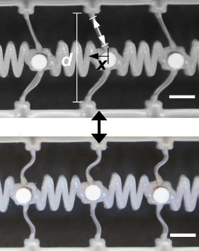
The Harvard/Caltech system for transmitting a mechanical signal consists of a series of bistable elements (the vertical beam, d, shown here) connected by soft coupling elements (wiggly lines), with two stable states. (Top) When a beam is displaced (by amount x), it stores energy. (Bottom) When it snaps back, it releases that stored energy into the coupling element on the right, which continues down the line, like dominos. (Scale bars represent 5 mm.) (credit: Jordan R. Raney/PNAS)

A new way to send mechanical signals through soft robots and other autonomous soft systems has been developed by researchers at the Harvard John A. Paulson School of Engineering and Applied Sciences (SEAS), in collaboration with colleagues at the California Institute of Technology, described in the journal Proceedings of the National Academy of Sciences.

Soft autonomous systems, just like the human body, can perform delicate movements that are safe for humans, unlike mechanical actuators controlled by wires. The problem is that in sending a mechanical signal through a soft material — to make a robot “muscle” move, for example — the signal becomes dissipated (weakened) and dispersed (scattered).

Think tapping on a solid wall to communicate via morse code with someone in the next room vs. tapping out a muffled message on a wall covered with thick, soft foam.

Transmitting signals through soft materials

The researchers solved this problem by using “bistable beams” (structures that function in two distinct states) to store and release elastic energy along the path of a wave.

This new system consists of a chain of bistable elastomeric (rubber-like) beam structures connected by elastomeric linear springs. When a beam is deformed (bent), it snaps and stores energy. As the signal travels along the elastomer, it snaps the beam back into place, releasing the beam’s stored energy and sending the signal downstream, like a line of dominos. This simple bistable system prevents the signal from dissipating downstream.

“This design solves two fundamental problems in transmitting information through materials,” said Katia Bertoldi, the John L. Loeb Associate Professor of the Natural Sciences at SEAS and senior author of the paper.  “It not only overcomes dissipation, but it also eliminates dispersive [spreading out] effects, so that the signal propagates without distortion.  As such, we maintain signal strength and clarity from start to end.” The team used advanced 3D printing techniques to fabricate the system.

Soft diodes and logic gates

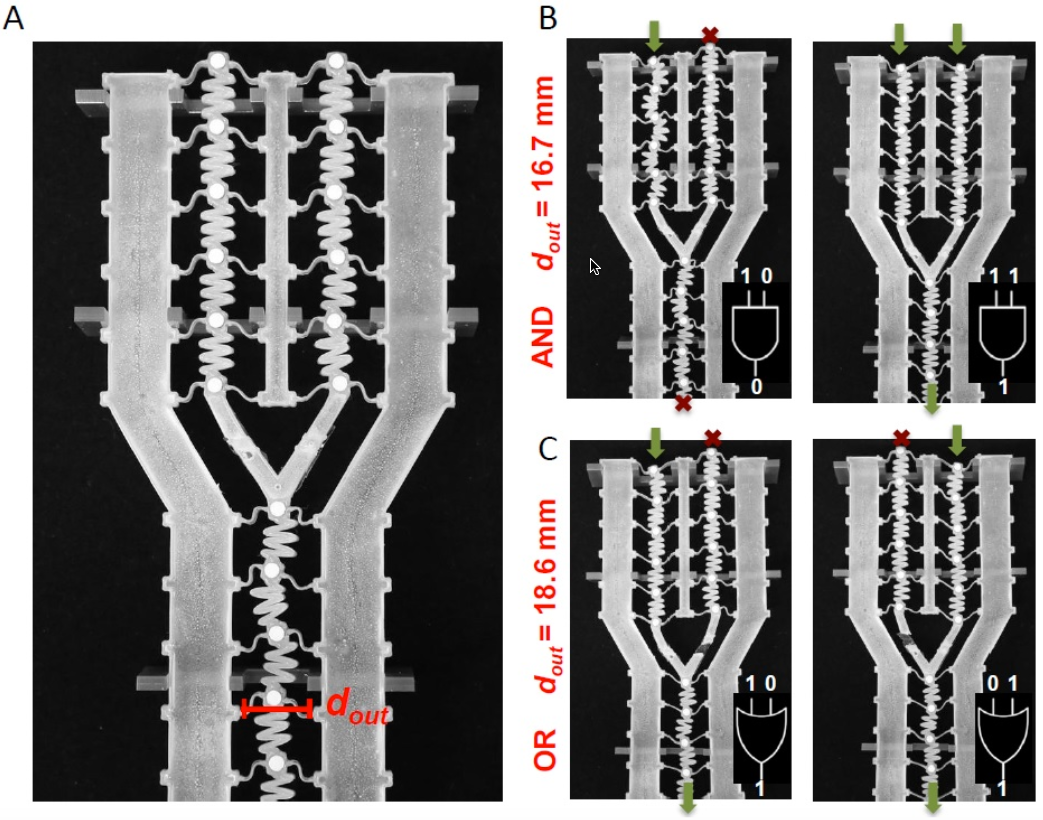
(A) A bifurcated (split into two) signal chain demonstrating tunable logic in a soft mechanical system. The distance d(out) determines the logical behavior, producing either an AND or an OR gate from the same system. (B) When d(out) is small (in this case, 16.7 mm) the energy barrier is higher, so both input signals must be strong to enable the wave to propagate through the output — a logical AND gate; (C) By increasing d(out) (to 18.6 mm in this case), the energy barrier decreases, producing a logical OR gate; in which case, either (or both) input signal has sufficient energy to trigger an output signal. (credit: Jordan R. Raney/PNAS)

The team also took the system a step further, designing and 3D-printing soft diodes and logic gates (a basic computational element that is normally part of a computer chip) using this same signal-transmission design. The gate can be controlled to act either as an AND (both inputs must be present to trigger the gate to fire) or as an OR gate (either one or both will trigger the gate to fire).

This research was supported by the National Science Foundation and the Harvard University Materials Research Science and Engineering Center (MRSEC).


Abstract of Stable propagation of mechanical signals in soft media using stored elastic energy

Soft structures with rationally designed architectures capable of large, nonlinear deformation present opportunities for unprecedented, highly-tunable devices and machines. However, the highly-dissipative nature of soft materials intrinsically limits or prevents certain functions, such as the propagation of mechanical signals. Here, we present an architected soft system comprised of elastomeric bistable beam elements connected by elastomeric linear springs. The dissipative nature of the polymer readily damps linear waves, preventing propagation of any mechanical signal beyond a short distance, as expected. However, the unique architecture of the system enables propagation of stable, nonlinear solitary transition waves with constant, controllable velocity and pulse geometry over arbitrary distances. Since the high damping of the material removes all other linear, small amplitude excitations, the desired pulse propagates with high delity and controllability. This phenomenon can be used to control signals, as demonstrated by the design of soft mechanical diodes and logic gates.