Self-propelling liquid metals: the future of soft electronics?

Liquid metal material with metallic core and semiconducting skin (credit: RMIT University)

Imagine a soft liquid-metal material right out of  the T-1000 Terminator movie character. One that can morph itself into different self-propelling soft electronic circuits that act like live cells, communicating with each other.

Using a liquid metallic core* and semiconducting skin, such a soft material might be used to make instant flexible 3D electronic displays. Or morph into self-propelled biomedical diagnostic sensors, for example, reconfiguring themselves on demand, say RMIT University researchers.
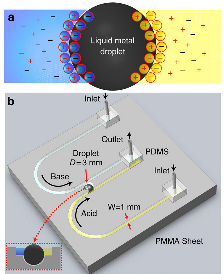
Diagram of ionic-imbalance-induced self-propulsion of liquid metals. (a) Schematic of the droplet and arrangement of ions, forming the EDL. (b) Schematic of the experimental setup showing two U-shaped open-top (see inset) inlet channels, which extend in parallel and join at an outlet. Two channels carry different types of electrolytes (acidic in yellow and basic in blue). Two parallel flows come in contact with the Galinstan droplet (3 mm diameter) residing in a recess. (credit: Ali Zavabeti et al./Nature Communications)

Morphing metal — more like live cells

To achieve that magic, Professor Kourosh Kalantar-zadeh and his group first immersed liquid-metal droplets in water. The droplets were able to move about freely in three dimensions, driven by pH (acid or base) or ionic (electric charge) concentration gradients across a liquid metal droplet, which induced deformation and surface flow.

“We adjusted the concentrations of acid, base, and salt components in the water and investigated the effect. Simply tweaking the water’s chemistry made the liquid metal droplets move and change shape, without any need for external mechanical, electronic, or optical stimulants.”
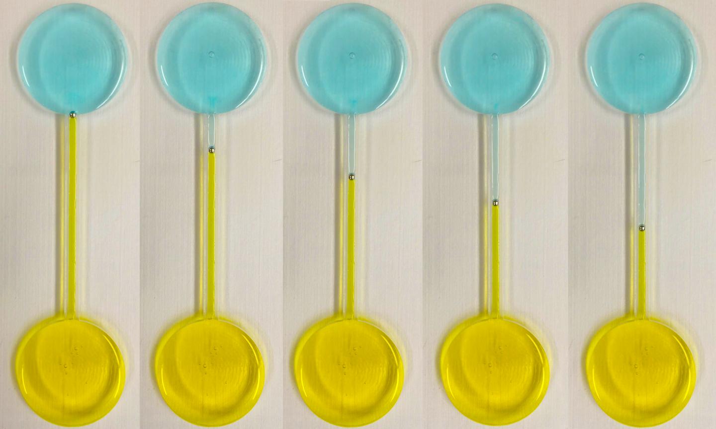
No, these are not lollipops. These devices demonstrate continuous motion of a self-propelling liquid metal droplet under a pH gradient, shown at different time intervals (left to right). The droplet is placed in a fluidic channel, midway between two reservoirs filled with different acid and base electrolytes. (credit: RMIT University)

The elastic electronic soft circuit systems act more like live cells, moving around autonomously and communicating with each other to form new circuits, rather than being stuck in one configuration.

“Using this discovery, we were able to create moving objects, switches, and pumps that could operate autonomously — self-propelling liquid metals driven by the composition of the surrounding fluid,” Kalantar-zadeh said. “Eventually, using the fundamentals of this discovery, it may be possible to build a 3D liquid metal humanoid on demand.”

The research was published August 4 in open-access Nature Communications.

* Galinstan, an alloy of of 68.5% gallium, 21.5% indium, and 10% tin, is used as the model liquid metal. Galinstan’s melting point can be lowered to below 0 °C (32 °F).


RMIT University | Liquid metals propel future electronics | RMIT University


Abstract of Ionic imbalance induced self-propulsion of liquid metals

Components with self-propelling abilities are important building blocks of small autonomous systems and the characteristics of liquid metals are capable of fulfilling self-propulsion criteria. To date, there has been no exploration regarding the effect of electrolyte ionic content surrounding a liquid metal for symmetry breaking that generates motion. Here we show the controlled actuation of liquid metal droplets using only the ionic properties of the aqueous electrolyte. We demonstrate that pH or ionic concentration gradients across a liquid metal droplet induce both deformation and surface Marangoni flow. We show that the Lippmann dominated deformation results in maximum velocity for the self-propulsion of liquid metal droplets and illustrate several key applications, which take advantage of such electrolyte-induced motion. With this finding, it is possible to conceive the propulsion of small entities that are constructed and controlled entirely with fluids, progressing towards more advanced soft systems.

IBM scientists emulate neurons with phase-change technology

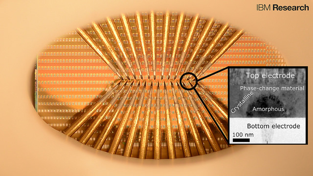
A prototype chip with large arrays of phase-change devices that store the state of artificial neuronal populations in their atomic configuration. The devices are accessed via an array of probes in this prototype to allow for characterization and testing. The tiny squares are contact pads used to access the nanometer-scale phase-change cells (inset).  Each set of probes can access a population of 100 cells. There are thousands to millions of these cells on one chip and IBM accesses them (in this particular photograph) by means of the sharp needles (probe card). (credit: IBM Research)

Scientists at IBM Research in Zurich have developed artificial neurons that emulate how neurons spike (fire). The goal is to create energy-efficient, high-speed, ultra-dense integrated neuromorphic (brain-like) technologies for applications in cognitive computing, such as unsupervised learning for detecting and analyzing patterns.

Applications could include internet of things sensors that collect and analyze volumes of weather data for faster forecasts and detecting patterns in financial transactions, for example.

The results of this research appeared today (Aug. 3) as a cover story in the journal Nature Nanotechnology.

Emulating neuron spiking

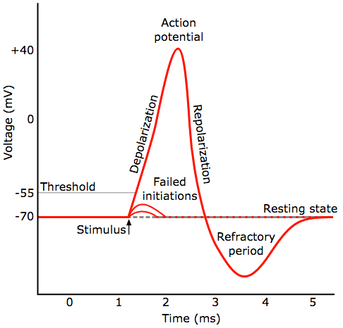
General pattern of a neural spike (action potential). A neuron fires (generates a rapid action potential, or voltage, when triggered by a stimulus) a signal from a synapse (credit: Chris 73/Diberri CC)

IBM’s new neuron-like spiking mechanism is based on a recent IBM breakthrough in phase-change materials. Phase-change materials are used for storing and processing digital data in re-writable Blu-ray discs, for example. The new phase-change materials developed by IBM recently are used instead for storing and processing analog data — like the synapses and neurons in our biological brains.

The new phase-change materials also overcome  problems in conventional computing, where there’s a separate memory and logic unit, slowing down computation. These functions are combined in the new artificial neurons, just as they are in a biological neuron.

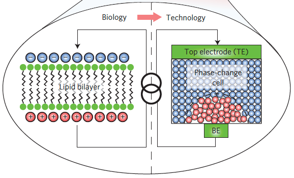
In biological neurons, a thin lipid-bilayer membrane separates the electrical charges inside the cell from those outside it. The membrane potential is altered by the arrival of excitatory and inhibitory postsynaptic potentials through the dendrites of the neuron, and upon sufficient excitation of the neuron (a phase change), an action potential, or spike, is generated. IBM’s new germanium-antimony-tellurium (GeSbTe or GST) phase-change material emulates this process. It has two stable states: an amorphous one (without a clearly defined structure) and a crystalline one (with a structure). (credit: Tomas Tuma et al./Nature Nanotechnology)

Alternative to von-Neumann-based algorithms

In addition, previous attempts to build artificial neurons are built using CMOS-based circuits, the standard transistor technology we have in our computers. The new phase-change technology can reproduce similar functionality at reduced power consumption. The artificial neurons are also superior in functioning at nanometer-length-scale dimensions and feature native stochasticity (based on random variables, simulating neurons).

“Populations of stochastic phase-change neurons, combined with other nanoscale computational elements such as artificial synapses, could be a key enabler for the creation of a new generation of extremely dense neuromorphic computing systems,” said Tomas Tuma, a co-author of the paper.

“The relatively complex computational tasks, such as Bayesian inference, that stochastic neuronal populations can perform with collocated processing and storage render them attractive as a possible alternative to von-Neumann-based algorithms in future cognitive computers,” the IBM scientists state in the paper.

IBM scientists have organized hundreds of these artificial neurons into populations and used them to represent fast and complex signals. These artificial neurons have been shown to sustain billions of switching cycles, which would correspond to multiple years of operation at an update frequency of 100 Hz. The energy required for each neuron update was less than five picojoule and the average power less than 120 microwatts — for comparison, 60 million microwatts power a 60 watt lightbulb.


IBM Research | All-memristive neuromorphic computing with level-tuned neurons


Abstract of Stochastic phase-change neurons

Artificial neuromorphic systems based on populations of spiking neurons are an indispensable tool in understanding the human brain and in constructing neuromimetic computational systems. To reach areal and power efficiencies comparable to those seen in biological systems, electroionics-based and phase-change-based memristive devices have been explored as nanoscale counterparts of synapses. However, progress on scalable realizations of neurons has so far been limited. Here, we show that chalcogenide-based phase-change materials can be used to create an artificial neuron in which the membrane potential is represented by the phase configuration of the nanoscale phase-change device. By exploiting the physics of reversible amorphous-to-crystal phase transitions, we show that the temporal integration of postsynaptic potentials can be achieved on a nanosecond timescale. Moreover, we show that this is inherently stochastic because of the melt-quench-induced reconfiguration of the atomic structure occurring when the neuron is reset. We demonstrate the use of these phase-change neurons, and their populations, in the detection of temporal correlations in parallel data streams and in sub-Nyquist representation of high-bandwidth signals.

New nanomaterial mimics cell membranes

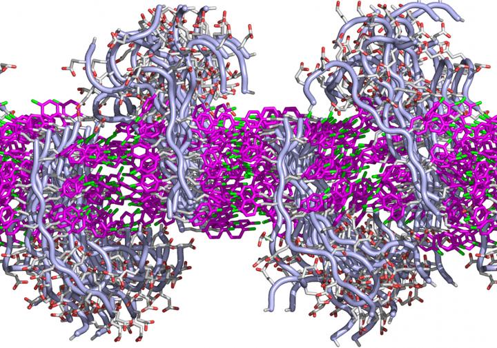
This simulated cross-section shows how the lipid-like peptoids interact to form a membrane. Each peptoid has two sections: a fatty-like region that interacts via benzene rings (shown in pink) with its neighbors to form a sheet, and a water-loving region that juts above or below the flat sheet. Each region can be designed to have specific functions. (credit: Chun-Long Chen/PNNL)

Materials scientists at the Department of Energy’s Pacific Northwest National Laboratory have created a new material that performs like a biological cell membrane — a material that has long been sought for applications like water purification and drug delivery.

The “peptoid” material can assemble itself into a sheet that’s thinner, but more stable, than a soap bubble, the researchers report this week in Nature Communications. The assembled sheet can withstand being submerged in a variety of liquids and can even repair itself after damage.

“We believe these materials have potential in water filters, sensors, drug delivery, and especially fuel cells or other energy applications,” said chemist Chun-Long Chen.

Biological cell membranes, which are made from thin sheets of fatty molecules called lipids, are at least ten times thinner than an iridescent soap bubble and yet allow cells to collectively form organisms as diverse at bacteria, trees and people.

Cell membranes are also very selective about what they let pass through, using tiny embedded proteins as gatekeepers. Membranes repair dings to their structure automatically and change thickness to pass signals from the outside environment to the cell’s interior, where most of the action is.

Scientists would like to take advantage of these gatekeeping and other membrane properties to make filters. A cell-membrane-like material would have advantages over other thin materials such as graphene. For example, mimicking a cell membrane’s efficient gatekeeping could result in water purifying membranes that don’t require a lot of pressure or energy to push the water through.

How to design imitation biological cell membranes

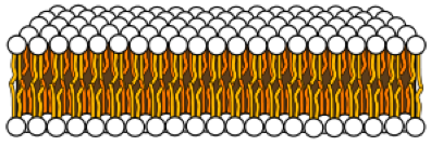
Lipid bilayer sheet (credit: Mariana Ruiz Villarreal/Wikipedia)

Synthetic molecules called peptoids have caught the interest of researchers because they are cheap, versatile and customizable. They are like natural proteins, including those that embed themselves in cell membranes, and can be designed to have very specific forms and functions. So Chen and colleagues decided to see if they could design peptoids to make them more lipid-like (that is, more like fats).

Lipid molecules are long and mostly straight: They have a fatty end that prefers to hang out with other fats, and a water-like end that prefers the comfort of water. Because of this chemistry, lipid molecules arrange themselves with the fatty ends pointed toward each other, sandwiched between the water-loving ends pointed out. Scientists call this a lipid bilayer, essentially a sheet that envelops the contents of a cell. Proteins or carbohydrate molecules embed themselves in the membranous sheet.

Inspired by this, Chen and colleagues designed peptoids in which each base peptoid was a long molecule with one end water-loving and the other end fat-loving. They chose chemical features that they hoped would encourage the individual molecules to pack together. They examined the resulting structures using a variety of analysis methods, including some at the Advanced Light Source and the Molecular Foundry, two DOE Office of Science User Facilities at Lawrence Berkeley National Laboratory.

Forming nanomembranes

Peptoid nanomembrane (credit: Haibao Jin et al./Nature Communications)

The team found that after putting the lipid-like peptoids into a liquid solution, the molecules spontaneously crystallized and formed “nanomembranes” — straight-edged sheets as thin as cell membranes — floating in the beaker. These nanomembranes maintained their structure in water or alcohol, at different temperatures, in solutions with high or low pH, or high concentrations of salts, a feat that few cell membranes could accomplish.

To better understand the nanomembranes, the team simulated how single peptoid molecules interacted with each other using molecular dynamics software. The simulated peptoids formed a membrane reminiscent of a lipid bilayer: The fat-loving ends lined up in the middle, and their water-loving ends pointed outward either above or below.

They also confirmed the ability of the synthetic membranes to hold proteins that have specific functions, such as ones that let water, and only water, through, and to repair themselves.

The results showed the researchers that they are on the right path to making synthetic cell membrane-like materials. The next step, Chen said, is to build biomimetic membranes by incorporating natural membrane proteins or other synthetic water channels such as carbon nanotubes into these sheet matrices. The team is also looking into ways to make the peptoid membranes conductive for energy uses.

This work was supported by the Department of Energy Office of Science and PNNL.


Abstract of Highly stable and self-repairing membrane-mimetic 2D nanomaterials assembled from lipid-like peptoids

An ability to develop sequence-defined synthetic polymers that both mimic lipid amphiphilicity for self-assembly of highly stable membrane-mimetic 2D nanomaterials and exhibit protein-like functionality would revolutionize the development of biomimetic membranes. Here we report the assembly of lipid-like peptoids into highly stable, crystalline, free-standing and self-repairing membrane-mimetic 2D nanomaterials through a facile crystallization process. Both experimental and molecular dynamics simulation results show that peptoids assemble into membranes through an anisotropic formation process. We further demonstrated the use of peptoid membranes as a robust platform to incorporate and pattern functional objects through large side-chain diversity and/or co-crystallization approaches. Similar to lipid membranes, peptoid membranes exhibit changes in thickness upon exposure to external stimuli; they can coat surfaces in single layers and self-repair. We anticipate that this new class of membrane-mimetic 2D nanomaterials will provide a robust matrix for development of biomimetic membranes tailored to specific applications.

Peering into atomically thin transistors with microwaves, scientists make a radical discovery: a one-dimensional transistor

Peering into an atomically thin semiconductor device with a “microwave microscope” via an AFM tip (credit: University of Texas at Austin)

Physicists at The University of Texas at Austin have had the first-ever glimpse into what happens inside an atomically thin semiconductor device. In doing so, they discovered that a transistor may be possible within a space so small (the edge) that it’s effectively one-dimensional.

Future tech innovations will require finding a way to fit more transistors on computer chips to keep up with Moore’s law, so experts have begun exploring new semiconducting materials, including one called molybdenum disulfide (MoS2), as KurzweilAI reported last week. In a paper published July 18 in the Proceedings of the National Academy of Sciencesthe researchers describe seeing the detailed inner workings of this new type of two-dimensional transistor.

Unlike today’s silicon-based devices, transistors made from MoS2 allow for on-off signaling on a single 2-D (flat) plane.

Computing on a one-dimensional edge

Keji Lai*, an assistant professor of physics, and his team used a “microwave impedance microscope” that he invented and that pointed microwaves at the 2-D device. Using an atomic force microscope (AFM) tip only 100 nanometers wide, the microwave microscope allowed the scientists to see conductivity changes inside the transistor for the first time.

That’s when they discovered that with MoS2, the conductive signaling happens much differently than with silicon — in a way that could promote future energy savings in devices.

With silicon transistors, the entire device is either turned on or off. With 2-D transistors, by contrast, Lai and the team found that electric currents move in a more phased (or wave-like) way, beginning first at the edges before appearing in the interior. Lai says this suggests the same current could be sent with less power and in an even tinier space — using a one-dimensional edge (a line) instead of the two-dimensional plane (area).

“In physics, edge states often carry a lot of interesting phenomena, and here, they are the first to turn on. In the future, if we can engineer this material very carefully, then these edges can carry the full current,” Lai says. “We don’t really need the entire thing, because the interior is useless. Just having the edges running to get a current working would substantially reduce the power loss.”

Eliminating defects

Researchers have been working to get a view into what happens inside a 2-D transistor for years to better understand both the potential and the limitations of the new materials. Getting 2-D transistors ready for commercial devices, such as paper-thin computers and cellphones, is expected to take several more years. Lai says scientists need more information about what interferes with performance in devices made from the new materials.

Besides seeing the currents’ motion, the scientists found thread-like defects in the middle of the transistors. Lai says this suggests the new material will need to be made cleaner to function optimally. “If we could make the material clean enough, the edges will be carrying even more current, and the interior won’t have as many defects,” Lai says.

The research was supported by the U.S. Department of Energy, the Welch Foundation, the Office of Naval Research, and the National Science Foundation.

* Earlier this year, Lai and co-researcher Deji Akinwande, associate professor of UT Austin’s Department of Electrical and Computer Engineering, won Presidential Early Career Awards for Scientists and Engineers, the U.S. government’s highest honor for early-stage scientists and engineers.


UT | In this visualization of what happens inside a 2-D transistor made of a promising new material called MoS2, electric currents appear initially at the outer edges and then inside of the device. Thread-like flaws can be seen in the interior part of the transistor.


Abstract of Uncovering edge states and electrical inhomogeneity in MoS2 field-effect transistors

The understanding of various types of disorders in atomically thin transition metal dichalcogenides (TMDs), including dangling bonds at the edges, chalcogen deficiencies in the bulk, and charges in the substrate, is of fundamental importance for TMD applications in electronics and photonics. Because of the imperfections, electrons moving on these 2D crystals experience a spatially nonuniform Coulomb environment, whose effect on the charge transport has not been microscopically studied. Here, we report the mesoscopic conductance mapping in monolayer and few-layer MoS2 field-effect transistors by microwave impedance microscopy (MIM). The spatial evolution of the insulator-to-metal transition is clearly resolved. Interestingly, as the transistors are gradually turned on, electrical conduction emerges initially at the edges before appearing in the bulk of MoS2 flakes, which can be explained by our firstprinciples calculations. The results unambiguously confirm that the contribution of edge states to the channel conductance is significant under the threshold voltage but negligible once the bulk of the TMD device becomes conductive. Strong conductance inhomogeneity, which is associated with the fluctuations of disorder potential in the 2D sheets, is also observed in the MIM images, providing a guideline for future improvement of the device performance.

World’s smallest storage device writes information atom by atom

STM scan (96 nm wide, 126 nm tall) of the 1 kB memory, written to a section of Feynman’s lecture, “There’s Plenty of Room at the Bottom” (credit: TU Delft/Ottelab)

Scientists at Kavli Institute of Nanoscience at Delft University have built a nanoscale data storage device containing 1 kilobyte (8,000 bits) with a storage density of 500 terabits per square inch (Tbpsi) — 500 times denser than the best commercial hard disk drive currently available. Each bit is represented by the position of one single chlorine atom.

“In theory, this storage density would allow all books ever created by humans to be written on a single post stamp,” says lead scientist Sander Otte. The research is reported today (Monday July 18) in Nature Nanotechnology.

Every day, modern society creates more than a billion gigabytes of new data. To store all this data, it is increasingly important that each single bit occupies as little space as possible.

In 1959, physicist Richard Feynman challenged his colleagues to engineer the world at the smallest possible scale. In his famous lecture There’s Plenty of Room at the Bottom, he speculated that if we had a platform allowing us to arrange individual atoms in an exact orderly pattern, it would be possible to store one piece of information per atom. To honor the visionary Feynman, Otte and his team have coded a section of Feynman’s lecture on an area 100 nanometers wide.

“Sliding puzzle” scheme

Atomic data storage scheme (credit: Kavli Institute of Nanoscience)

The team used a scanning tunneling microscope (STM), in which a sharp needle probes the atoms of a surface, one by one. With these probes scientists can see atoms and push them around. “You could compare it  to a sliding puzzle,” Otte explains. “Every bit consists of two positions on a surface of copper atoms, and one chlorine atom that we can slide back and forth between these two positions. If the chlorine atom is in the top position, there is a hole beneath it — we call this a 1. If the hole is in the top position and the chlorine atom is therefore on the bottom, then the bit is a 0.”

Because the chlorine atoms are surrounded by other chlorine atoms, except near the holes, they keep each other in place. Which is why this method with holes is much more stable than methods with loose atoms and more suitable for data storage.

Kilobyte atomic memory. 1,016-byte atomic memory, written to a passage from Feynman’s lecture, “There’s plenty of room at the bottom.” The memory consists of 127 functional blocks and 17 broken blocks, resulting in an overall areal density of 0.778 bits per nm square. (credit: F. E. Kalff et al./Nature Nanotechnology)

The researchers organized their memory in blocks of 8 bytes (64 bits). Each block has a marker, made of the same type of “holes” as the raster of chlorine atoms. Inspired by the pixelated square barcodes (QR codes) often used to scan tickets for airplanes and concerts, these markers work like miniature QR codes that carry information about the precise location of the block on the copper layer. The code will also indicate if a block is damaged, for instance due to some local contaminant or an error in the surface. This allows the memory to be scaled up easily to very big sizes, even if the copper surface is not entirely perfect.

The new approach offers excellent prospects in terms of stability and scalability. However, “in its current form the memory can operate only in very clean vacuum conditions and at liquid nitrogen temperature (77 K), so the actual storage of data on an atomic scale is still some way off.”

This research was support by the Netherlands Organisation for Scientific Research (NOW/FOM). Scientists of the International Iberian Nanotechnology Laboratory (INL) in Portugal performed calculations on the behavior of the chlorine atoms.


Delft University of Technology | Atomic scale data storage


Abstract of A kilobyte rewritable atomic memory

The advent of devices based on single dopants, such as the single-atom transistor, the single-spin magnetometer and the single-atom memory, has motivated the quest for strategies that permit the control of matter with atomic precision. Manipulation of individual atoms by low-temperature scanning tunnelling microscopy provides ways to store data in atoms, encoded either into their charge state, magnetization state or lattice position. A clear challenge now is the controlled integration of these individual functional atoms into extended, scalable atomic circuits. Here, we present a robust digital atomic-scale memory of up to 1 kilobyte (8,000 bits) using an array of individual surface vacancies in a chlorine-terminated Cu(100) surface. The memory can be read and rewritten automatically by means of atomic-scale markers and offers an areal density of 502 terabits per square inch, outperforming state-of-the-art hard disk drives by three orders of magnitude. Furthermore, the chlorine vacancies are found to be stable at temperatures up to 77 K, offering the potential for expanding large-scale atomic assembly towards ambient conditions.

DNA origami creates a microscopic glowing Van Gogh

This reproduction of van Gogh’s The Starry Night contains 65,536 glowing pixels but is just the width of a dime across, as a proof-of-concept of precision placement of DNA origami (credit: Paul Rothemund and Ashwin Gopinath/Caltech)

Using folded DNA to precisely place glowing molecules within microscopic light resonators, researchers at Caltech have created one of the world’s smallest reproductions of Vincent van Gogh’s The Starry Night. The feat is a proof-of-concept of how precision placement of DNA origami can be used to build hybrid nanophotonic devices at smaller scales than ever before.

DNA origami, developed 10 years ago by Caltech’s research professor Paul Rothemund, is a technique that allows researchers to fold (in a test tube) a long strand of self-assembling DNA into any desired shape. The folded DNA then acts as a scaffold (support) onto which researchers can attach nanometer-scale components. KurzweilAI has reported extensively on DNA origami — most recently, an automated design method for creating nanoparticles for drug delivery and cell targeting, nanoscale robots, custom-tailored optical devices, and DNA as a data storage medium, for example.

Meanwhile, over the last seven years, Rothemund and associates have refined and extended DNA orgami so that DNA shapes can be precisely positioned on almost any surface used in the manufacture of computer chips. Now, in a Nature paper on July 11, they report the first application of the technique — using DNA origami to install fluorescent molecules into microscopic light sources for use in single-molecule detection, quantum computers, and other applications.

The work was supported by the Army Research Office, the Office of Naval Research, the Air Force Office of Scientific Research, and the National Science Foundation.


Abstract of Engineering and mapping nanocavity emission via precision placement of DNA origami

Many hybrid devices integrate functional molecular or nanoparticle components with microstructures, as exemplified by the nanophotonic devices that couple emitters to optical resonators for potential use in single-molecule detection, precision magnetometry, low threshold lasing and quantum information processing. These systems also illustrate a common difficulty for hybrid devices: although many proof-of-principle devices exist, practical applications face the challenge of how to incorporate large numbers of chemically diverse functional components into microfabricated resonators at precise locations. Here we show that the directed self-assembly of DNA origami onto lithographically patterned binding sites allows reliable and controllable coupling of molecular emitters to photonic crystal cavities (PCCs). The precision of this method is sufficient to enable us to visualize the local density of states within PCCs by simple wide-field microscopy and to resolve the antinodes of the cavity mode at a resolution of about one-tenth of a wavelength. By simply changing the number of binding sites, we program the delivery of up to seven DNA origami onto distinct antinodes within a single cavity and thereby digitally vary the intensity of the cavity emission. To demonstrate the scalability of our technique, we fabricate 65,536 independently programmed PCCs on a single chip. These features, in combination with the widely used modularity of DNA origami, suggest that our method is well suited for the rapid prototyping of a broad array of hybrid nanophotonic devices.

A biocompatible, transparent therapeutic window to the brain

An illustration showing how the “window to the brain” transparent skull implant created by UC Riverside researchers would work (credit: UC Riverside)

Researchers at the University of California, Riverside have developed a transparent “window to the brain” — a skull implant that is biocompatible, infection-resistant, and does not need to be repetitively replaced.

Part of the ongoing “Window to the Brain” project, a multi-institution, cross-disciplinary effort, the idea is to use transparent skull implants to provide laser diagnosis and treatment of a wide variety of brain pathologies, including brain cancers, traumatic brain injury, stroke, and neurodegenerative diseases, without requiring repeated craniotomies (a surgical operation in which a bone flap is temporarily removed from the skull to access the brain). Such operations are vulnerable to bacterial infections.

A biocompatible transparent material

The researchers have developed a transparent version of the material yttria-stabilized zirconia (YSZ), a ceramic material used in hip implants and dental crowns.

The researchers implanted the material in a hamster, where it integrated into the host tissue without causing an immune response or other adverse effects, as they describe in a paper in the journal Nanomedicine: Nanotechnology, Biology and Medicine. The internal toughness of YSZ, which is more impact-resistant and biocompatible than the titanium, thermoplastic polymers, and glass-based materials developed by other researchers, makes it “the only transparent skull implant that could conceivably be used in humans,” according to the researchers.

Treating bacterial infections

Schematic diagram showing treatment of biofilm formation with near-infrared laser light via a transparent YSZ material, monitored by a thermal IR camera (credit: Yasaman Damestani et al./Lasers in Surgery and Medicine)

The scientists also developed a way to use the same laser light used in brain treatments to treat incidental bacterial infections. In a lab study, described in a paper in the journal Lasers in Surgery and Medicine, the researchers treated E. Coli infections by aiming laser light through the transparent implant, without having to remove the implant and without causing an immune response or other adverse effects to surrounding tissue.

“This was an important finding because it showed that the combination of our transparent implant and laser-based therapies enables us to treat not only brain disorders, but also to tackle bacterial infections that are common after cranial implants. These infections are especially challenging to treat because many antibiotics do not penetrate the blood brain barrier,” said Devin Binder, M.D., a neurosurgeon and neuroscientist in UCR’s School of Medicine and a collaborator on the project.

The Window to the Brain project is a multi-institution, interdisciplinary partnership led by Guillermo Aguilar, professor of mechanical engineering in UCR’s Bourns College of Engineering, and Santiago Camacho-López, from the Centro de Investigación Científica y de Educación Superior de Ensenada (CICESE) in Mexico.

Last October, the team received $3.6 million from the National Science Foundation’s Partnerships in International Research and Education (PIRE) program, which pairs U.S. universities with others around the world. An additional $1 million was from Consejo Nacional de Ciencia y Tecnología (CONACYT), Mexico’s entity in charge of promoting scientific and technological activities. The remainder of the money came from in-kind contributions from the Mexican universities.

The team’s long-term goal is to see the technology become the standard of care for patients with brain disorders.


Abstract of Inflammatory response to implantation of transparent nanocrystalline yttria-stabilized zirconia using a dorsal window chamber model

The long-range goal of the windows to the brain (WttB) is to improve patient care by providing a technique for delivery and/or collection of light into/from the brain, on demand, over large areas, and on a chronically-recurring basis without the need for repeated craniotomies. To evaluate the potential of nanocrystalline yttria-stabilized-zirconia (nc-YSZ) cranial implant for optical therapy and imaging, in vivo biocompatibility was studied using the dorsal window chamber model in comparison with control (no implant) and commercially available cranial implant materials (PEEK and PEKK). The host tissue response to implant was characterized by using transillumination and fluorescent microscopy to measure leukocyte adhesion, blood vessel diameter, blood flow rate, and vascular permeability over two weeks. The results indicated the lack of inflammatory reaction of the host tissue to nc-YSZ at the microscopic level, suggesting that nc-YSZ is a good alternative material for cranial implants.


Abstract of Evaluation of laser bacterial anti-fouling of transparent nanocrystalline yttria-stabilized-zirconia cranial implant

Background and Objective: The development and feasibility of a novel nanocrystalline yttria-stabilized-zirconia (nc-YSZ) cranial implant has been recently established. The purpose of what we now call “window to the brain (WttB)” implant (or platform), is to improve patient care by providing a technique for delivery and/or collection of light into/from the brain, on demand, over large areas, and on a chronically recurring basis without the need for repeated craniotomies. WttB holds the transformative potential for enhancing light-based diagnosis and treatment of a wide variety of brain pathologies including cerebral edema, traumatic brain injury, stroke, glioma, and neurodegenerative diseases. However, bacterial adhesion to the cranial implant is the leading factor for biofilm formation (fouling), infection, and treatment failure. Escherichia coli (E. coli), in particular, is the most common isolate in gram-negative bacillary meningitis after cranial surgery or trauma. The transparency of our WttB implant may provide a unique opportunity for non-invasive treatment of bacterial infection under the implant using medical lasers.

Study Design/Materials and Methods: A drop of a diluted overnight culture of BL21-293 E. coli expressing luciferase was seeded between the nc-YSZ implant and the agar plate. This was followed by immediate irradiation with selected laser. After each laser treatment the nc-YSZ was removed, and cultures were incubated for 24 hours at 37 °C. The study examined continuous wave (CW) and pulsed wave (PW) modes of near-infrared (NIR) 810 nm laser wavelength with a power output ranging from 1 to 3 W. During irradiation, the temperature distribution of nc-YSZ surface was monitored using an infrared thermal camera. Relative luminescence unit (RLU) was used to evaluate the viability of bacteria after the NIR laser treatment.

Results: Analysis of RLU suggests that the viability of E. coli biofilm formation was reduced with NIR laser treatment when compared to the control group (P < 0.01) and loss of viability depends on both laser fluence and operation mode (CW or PW). The results demonstrate that while CW laser reduces the biofilm formation more than PW laser with the same power, the higher surface temperature of the implant generated by CW laser limits its medical efficacy. In contrast, with the right parameters, PW laser produces a more moderate photothermal effect which can be equally effective at controlling bacterial growth.

Conclusions: Our results show that E. coli biofilm formation across the thickness of the nc-YSZ implant can be disrupted using NIR laser treatment. The results of this in vitro study suggest that using nc-YSZ as a cranial implant in vivo may also allow for locally selective, non-invasive, chronic treatment of bacterial layers (fouling) that might form under cranial implants, without causing adverse thermal damage to the underlying host tissue when appropriate laser parameters are used. Lasers Surg. Med. © 2016 Wiley Periodicals, Inc.

Berkeley Lab scientists grow atomically thin transistors and circuits

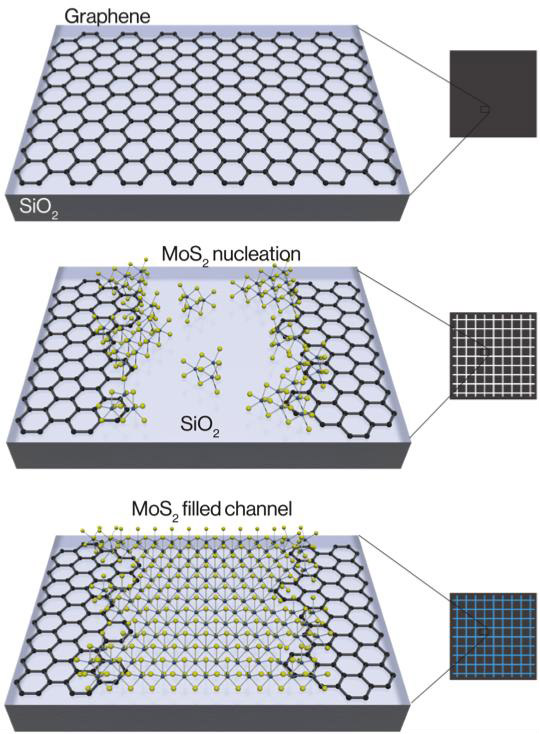
This schematic shows the chemical assembly of two-dimensional crystals. Graphene is first etched into channels and the TMDC molybdenum disulfide (MoS2) begins to nucleate around the edges and within the channel. On the edges, MoS2 slightly overlaps on top of the graphene. Finally, further growth results in MoS2 completely filling the channels. (credit: Berkeley Lab)

In an advance that helps pave the way for next-generation electronics and computing technologies — and possibly paper-thin devices — scientists with the U.S. Department of Energy’s Lawrence Berkeley National Laboratory (Berkeley Lab) have developed a way to chemically assemble transistors and circuits that are only a few atoms thick.

In addition, their method yields functional structures at a scale large enough to begin thinking about real-world applications and commercial scalability.

They reported their research online July 11 in the journal Nature Nanotechnology.

The scientists controlled the synthesis of a transistor in which narrow channels were etched onto conducting graphene, and a semiconducting material called a transition-metal dichalcogenide (TMDC) was seeded in the blank channels.

Both of these materials are single-layered crystals and atomically thin, so the two-part assembly yielded electronic structures that are essentially two-dimensional, and cover an area a few centimeters long and a few millimeters wide.

“This is a big step toward a scalable and repeatable way to build atomically thin electronics or pack more computing power in a smaller area,” says Xiang Zhang, a senior scientist in Berkeley Lab’s Materials Sciences Division who led the study.

Their work is part of a new wave of research aimed at keeping pace with Moore’s Law, which holds that the number of transistors in an integrated circuit doubles approximately every two years. To keep this pace, scientists predict that integrated electronics will soon require transistors that measure less than ten nanometers in length.

“With silicon, this will be extremely challenging, because the thickness of the transistor’s channel will become greater than the channel length, ultimately leading to difficult electrostatic control via the transistor gate,” the authors note. Nanomaterials such as inorganic nanowires and Stanford/IBM’s carbon nanotubes have been proposed, but require impractical “precise placement and orientation using complex fabrication techniques,” the authors point out.

The two-dimensional solution for keeping up with Moore’s law

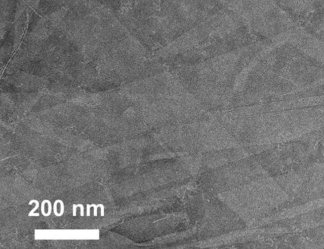
Optical image of the atomically thin graphene–MoS heterostructure. Arrows indicate nucleation (junctions) with graphene of the MoS2 areas, forming transistors. (credit: Mervin Zhao et al./Nature Nanotechnology)

So researchers have now looked to two-dimensional crystals that are only one molecule thick as alternative materials to keep up with Moore’s Law. Using that approach, the Berkeley Lab scientists developed a way to seed a single-layered semiconductor — in this case, the TMDC molybdenum disulfide (MoS2) — into channels lithographically etched within a sheet of conducting graphene. The two atomic sheets meet to form nanometer-scale junctions that make atomically thin transistors in which the graphene conductor efficiently injects current into the MoS2.

“This approach allows for the chemical assembly of electronic circuits, using two-dimensional materials, which show improved performance compared to using traditional metals to inject current into TMDCs,” says Mervin Zhao, a lead author and Ph.D. student in Zhang’s group at Berkeley Lab and UC Berkeley.

The scientists demonstrated the usefulness of the structure by assembling it into the logic circuitry of an inverter (NOT gate). This further underscores the technology’s ability to lay the foundation for a chemically assembled atomic computer, the scientists say. They also note that the two-dimensional crystals were synthesized at a wafer scale, so the scalable design is compatible with current semiconductor manufacturing.

The research was supported by the Office of Naval Research and the National Science Foundation. Scientists from Cornell University were also involved in the research.


Abstract of Large-scale chemical assembly of atomically thin transistors and circuits

Next-generation electronics calls for new materials beyond silicon, aiming at increased functionality, performance and scaling in integrated circuits. In this respect, two-dimensional gapless graphene and semiconducting transition-metal dichalcogenides have emerged as promising candidates due to their atomic thickness and chemical stability. However, difficulties with precise spatial control during their assembly currently impede actual integration into devices. Here, we report on the large-scale, spatially controlled synthesis of heterostructures made of single-layer semiconducting molybdenum disulfide contacting conductive graphene. Transmission electron microscopy studies reveal that the single-layer molybdenum disulfide nucleates at the graphene edges. We demonstrate that such chemically assembled atomic transistors exhibit high transconductance (10 µS), on–off ratio (∼106) and mobility (∼17 cm2 V−1 s−1). The precise site selectivity from atomically thin conducting and semiconducting crystals enables us to exploit these heterostructures to assemble two-dimensional logic circuits, such as an NMOS inverter with high voltage gain (up to 70).

Molecular flip in crystals driven by light creates microrobotic propulsion

(a) Sequential micrographs of one cycle of self-oscillation observed under 435-nm light and schematic illustrations. (b) Schematic illustration showing setup. (credit: Tomonori Ikegami et al./Angewandte Chemie)

Hokkaido University researchers have designed a crystal material that continually flips between two positions like a paddle, propelling an attached structure, when stimulated by blue light. It could lead to bio-inspired microrobots that deliver drugs to target tissues, for example.

The team made azobenzene-oleic acid crystals, composed of an organic compound called azobenzene, commonly used in dye manufacturing, and oleic acid, commonly found in cooking oil. Azobenzene molecules take two structurally different forms: cis and trans, and they were found to switch back and forth when stimulated by the light.

The frequency of the motion also increased with increased light intensity. Some crystal complexes they created even exhibited swimming-like motions in the water, the researchers report. Previously reported light-responsive materials have been limited in their ability to deform, the researchers noted.

“The importance of this study lies in the realization of macroscopic self-oscillation by the repeated reversible reaction of a molecular machine with the cooperative transformation of a molecular assembly,” the researchers note in a paper published in the journal Angewandte Chemie. “These results provide a fundamental strategy for constructing dynamic self-organizations in supramolecular systems to achieve bioinspired molecular systems.”


Ikegami T. et. al. | A crystalline assembly of azobenzene derivative and oleate showed oscillatory bending-unbending motion under continuous 435-nm light irradiation.


Abstract of Dissipative and Autonomous Square-Wave Self-Oscillation of a Macroscopic Hybrid Self-Assembly under Continuous Light Irradiation

Building a bottom-up supramolecular system to perform continuously autonomous motions will pave the way for the next generation of biomimetic mechanical systems. In biological systems, hierarchical molecular synchronization underlies the generation of spatio-temporal patterns with dissipative structures. However, it remains difficult to build such self-organized working objects via artificial techniques. Herein, we show the first example of a square-wave limit-cycle self-oscillatory motion of a noncovalent assembly of oleic acid and an azobenzene derivative. The assembly steadily flips under continuous blue-light irradiation. Mechanical self-oscillation is established by successively alternating photoisomerization processes and multi-stable phase transitions. These results offer a fundamental strategy for creating a supramolecular motor that works progressively under the operation of molecule-based machines.

The ‘ultimate discovery tool’ for nanoparticles

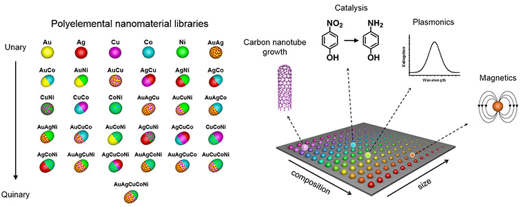
A combinatorial library of polyelemental nanoparticles was developed using Dip-Pen Nanolithography, opening up a new field of nanocombinatorics for rapid screening of nanomaterials for a multitude of properties. (credit: Peng-Cheng Chen/James Hedrick)

The discovery power of the gene chip is coming to nanotechnology, as a Northwestern University research team develops a  tool to rapidly test millions — and perhaps even billions — of different nanoparticles at one time to zero in on the best nanoparticle for a specific use.

When materials are miniaturized, their properties — optical, structural, electrical, mechanical and chemical — change, offering new possibilities. But determining what nanoparticle size and composition are best for a given application, such as catalysts, biodiagnostic labels, pharmaceuticals and electronic devices, is a daunting task.

“As scientists, we’ve only just begun to investigate what materials can be made on the nanoscale,” said Northwestern’s Chad A. Mirkin, a world leader in nanotechnology research and its application, who led the study. “Screening a million potentially useful nanoparticles, for example, could take several lifetimes. Once optimized, our tool will enable researchers to pick the winner much faster than conventional methods. We have the ultimate discovery tool.”

Combinatorial libraries of nanoparticles

Using a Northwestern technique that deposits materials on a surface, Mirkin and his team figured out how to make combinatorial libraries of nanoparticles in a controlled way. (A combinatorial library is a collection of systematically varied structures encoded at specific sites on a surface.) Their study was published today (June 24) by the journal Science.

The nanoparticle libraries are much like a gene chip, Mirkin says, where thousands of different spots of DNA are used to identify the presence of a disease or toxin. Thousands of reactions can be done simultaneously, providing results in just a few hours. Similarly, Mirkin and his team’s libraries will enable scientists to rapidly make and screen millions to billions of nanoparticles of different compositions and sizes for desirable physical and chemical properties.

“The ability to make libraries of nanoparticles will open a new field of nanocombinatorics, where size — on a scale that matters — and composition become tunable parameters,” Mirkin said. “This is a powerful approach to discovery science.”

Mirkin is the George B. Rathmann Professor of Chemistry in the Weinberg College of Arts and Sciences and founding director of Northwestern’s International Institute for Nanotechnology.

Using just five metallic elements — gold, silver, cobalt, copper and nickel — Mirkin and his team developed an array of unique structures by varying every elemental combination. In previous work, the researchers had shown that particle diameter also can be varied deliberately on the 1- to 100-nanometer length scale.

More than half never existed before on Earth

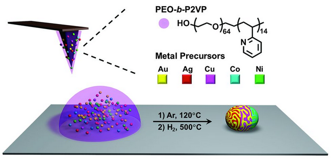
Synthesis of multimetallic NPs and a five-element library of unary and multimetallic NPs (credit: Peng-Cheng Chen et al./Science)

Some of the compositions can be found in nature, but more than half of them have never existed before on Earth. And when pictured using high-powered imaging techniques, the nanoparticles appear like an array of colorful Easter eggs, each compositional element contributing to the palette.

To build the combinatorial libraries, Mirkin and his team used Dip-Pen Nanolithography, a technique developed at Northwestern in 1999, to deposit onto a surface individual polymer “dots,” each loaded with different metal salts of interest. The researchers then heated the polymer dots, reducing the salts to metal atoms and forming a single nanoparticle. The size of the polymer dot can be varied to change the size of the final nanoparticle.

The researchers used the tool to systematically generate a library of 31 nanostructures using the five different metals. They then used  advanced electron microscopes to spatially map the compositional trajectories of the combinatorial nanoparticles.

The next materials to power fuel cells, efficiently harvest solar energy, or create new chips

Scientists can now begin to study these nanoparticles as well as build other useful combinatorial libraries consisting of billions of structures that subtly differ in size and composition. These structures may become the next materials that power fuel cells, efficiently harvest solar energy and convert it into useful fuels, and catalyze reactions that take low-value feedstocks from the petroleum industry and turn them into high-value products useful in the chemical and pharmaceutical industries.

Mirkin is a member of the Robert H. Lurie Comprehensive Cancer Center of Northwestern University as well as co-director of the Northwestern University Center for Cancer Nanotechnology Excellence. He also is a professor of medicine, chemical and biological engineering, biomedical engineering and materials science at Northwestern.

The research was supported by GlaxoSmithKline, the Air Force Office of Scientific Research,and the Asian Office of Aerospace R&D.


Abstract of Polyelemental nanoparticle libraries

Multimetallic nanoparticles are useful in many fields, yet there are no effective strategies for synthesizing libraries of such structures, in which architectures can be explored in a systematic and site-specific manner. The absence of these capabilities precludes the possibility of comprehensively exploring such systems. We present systematic studies of individual polyelemental particle systems, in which composition and size can be independently controlled and structure formation (alloy versus phase-separated state) can be understood. We made libraries consisting of every combination of five metallic elements (Au, Ag, Co, Cu, and Ni) through polymer nanoreactor–mediated synthesis. Important insight into the factors that lead to alloy formation and phase segregation at the nanoscale were obtained, and routes to libraries of nanostructures that cannot be made by conventional methods were developed.