The top 10 emerging technologies of 2016

(credit: WEF)

The World Economic Forum’s annual list of this year’s breakthrough technologies, published today, includes “socially aware” openAI, grid-scale energy storage, perovskite solar cells, and other technologies with the potential to “transform industries, improve lives, and safeguard the planet.” The WEF’s specific interest is to “close gaps in investment and regulation.”

“Horizon scanning for emerging technologies is crucial to staying abreast of developments that can radically transform our world, enabling timely expert analysis in preparation for these disruptors. The global community needs to come together and agree on common principles if our society is to reap the benefits and hedge the risks of these technologies,” said Bernard Meyerson, PhD, Chief Innovation Officer of IBM and Chair of the WEF’s Meta-Council on Emerging Technologies.

The list also provides an opportunity to debate human, societal, economic or environmental risks and concerns that the technologies may pose — prior to widespread adoption.

One of the criteria used by council members during their deliberations was the likelihood that 2016 represents a tipping point in the deployment of each technology. So the list includes some technologies that have been known for a number of years, but are only now reaching a level of maturity where their impact can be meaningfully felt.

The top 10 technologies that make this year’s list are:

  1. Nanosensors and the Internet of Nanothings  — With the Internet of Things expected to comprise 30 billion connected devices by 2020, one of the most exciting areas of focus today is now on nanosensors capable of circulating in the human body or being embedded in construction materials. They could use DNA and proteins to recognize specific chemical targets, store a few bits of information, and then report their status by changing color or emitting some other easily detectable signal.
  2. Next-Generation Batteries — One of the greatest obstacles holding renewable energy back is matching supply with demand, but recent advances in energy storage using sodium, aluminum, and zinc based batteries makes mini-grids feasible that can provide clean, reliable, around-the-clock energy sources to entire villages.
  3. The Blockchain — With venture investment related to the online currency Bitcoin exceeding $1 billion in 2015 alone, the economic and social impact of blockchain’s potential to fundamentally change the way markets and governments work is only now emerging.
  4. 2D Materials — Plummeting production costs mean that 2D materials like graphene are emerging in a wide range of applications, from air and water filters to new generations of wearables and batteries.
  5. Autonomous Vehicles — The potential of self-driving vehicles for saving lives, cutting pollution, boosting economies, and improving quality of life for the elderly and other segments of society has led to rapid deployment of key technology forerunners along the way to full autonomy.
  6. Organs-on-chips — Miniature models of human organs could revolutionize medical research and drug discovery by allowing researchers to see biological mechanism behaviors in ways never before possible.
  7. Perovskite Solar Cells — This new photovoltaic material offers three improvements over the classic silicon solar cell: it is easier to make, can be used virtually anywhere and, to date, keeps on generating power more efficiently.
  8. Open AI Ecosystem — Shared advances in natural language processing and social awareness algorithms, coupled with an unprecedented availability of data, will soon allow smart digital assistants to help with a vast range of tasks, from keeping track of one’s finances and health to advising on wardrobe choice.
  9. Optogenetics — Recent developments mean light can now be delivered deeper into brain tissue, something that could lead to better treatment for people with brain disorders.
  10. Systems Metabolic Engineering — Advances in synthetic biology, systems biology, and evolutionary engineering mean that the list of building block chemicals that can be manufactured better and more cheaply by using plants rather than fossil fuels is growing every year.

To compile this list, the World Economic Forum’s Meta-Council on Emerging Technologies, a panel of global experts, “drew on the collective expertise of the Forum’s communities to identify the most important recent technological trends. By doing so, the Meta-Council aims to raise awareness of their potential and contribute to closing gaps in investment, regulation and public understanding that so often thwart progress.”

You can read 10 expert views on these technologies here or download the series as a PDF.

How to convert graphene into a semiconductor for scalable production

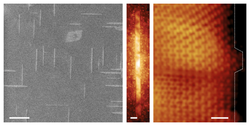
Progressively magnified images (left to right; scale bars: 400, 10, and 1 nm) of graphene nanoribbons grown on germanium semiconductor wafers.  (credit: Michael Arnold/University of Wisconsin-Madison)

Graphene can be transformed in the lab from a semimetal into a semiconductor if it is confined into nanoribbons narrower than 10 nm (with controlled orientation and edges), but scaling it up for commercial use has not been possible. Until now.

University of Wisconsin-Madison scientists have discovered how to synthesize narrow, long “one-dimensional” (1-D) nanoribbons (sub-10 nanometers wide) directly on a conventional germanium semiconductor wafer.

That narrow width is not possible with the optical and electron-beam lithography techniques conventionally used in making chips, and integrating graphene nanoribbons onto insulating or semiconducting wafers has also been difficult.

The breakthrough was extremely slow growth (under 5 nanometers per hour), using a new variation of a technique called chemical vapor deposition (CVD), allowing nanoribbons with length-to-width aspect ratios greater than 70 to grow on the surface of a germanium wafer (and with the required smooth “armchair” edges — see the image on the right above).

In addition, this new fabrication process is compatible with existing semiconductor fabrication infrastructure. Appears promising. Let’s see which chipmakers go for it.

The research is described in an open-access article just published in Nature Communications.


Abstract of Direct oriented growth of armchair graphene nanoribbons on germanium

Graphene can be transformed from a semimetal into a semiconductor if it is confined into nanoribbons narrower than 10 nm with controlled crystallographic orientation and well-defined armchair edges. However, the scalable synthesis of nanoribbons with this precision directly on insulating or semiconducting substrates has not been possible. Here we demonstrate the synthesis of graphene nanoribbons on Ge(001) via chemical vapour deposition. The nanoribbons are self-aligning 3° from the Geleft fence110right fence directions, are self-defining with predominantly smooth armchair edges, and have tunable width to <10 nm and aspect ratio to >70. In order to realize highly anisotropic ribbons, it is critical to operate in a regime in which the growth rate in the width direction is especially slow, <5 nm h−1. This directional and anisotropic growth enables nanoribbon fabrication directly on conventional semiconductor wafer platforms and, therefore, promises to allow the integration of nanoribbons into future hybrid integrated circuits.
First self-driving ‘cognitive’ vehicle uses IBM Watson Internet of Things

Olli (credit: Local Motors)

Local Motors, creator of the world’s first 3D-printed cars, has developed the first self-driving “cognitive” vehicle, using IBM Watson Internet of Things (IoT) for Automotive.

The vehicle, dubbed “Olli,” can carry up to 12 people. It uses IBM Watson and other systems to improve the passenger experience and allow natural interaction with the vehicle. Olli will be used on public roads locally in Washington DC and later this year in Miami-Dade County.

Olli is the first vehicle to use the cloud-based cognitive computing capability of IBM Watson IoT to analyze and learn from high volumes of transportation data, produced by more than 30 sensors embedded throughout the vehicle. Sensors will be added and adjusted continually as passenger needs and local preferences are identified.

Four Watson developer APIs — Speech to Text, Natural Language Classifier, Entity Extraction and Text to Speech — will enable passengers to interact conversationally with Olli while traveling from point A to point B, discussing topics about how the vehicle works, where they are going, and why Olli is making specific driving decisions.

Watson empowers Olli to understand and respond to passengers’ questions as they enter the vehicle, such as destinations (“Olli, can you take me downtown?”) or specific vehicle functions (“how does this feature work?” or even “are we there yet?”). Passengers can also ask for recommendations on local destinations such as popular restaurants or historical sites based on analysis of personal preferences.

“Cognitive computing provides incredible opportunities to create unparalleled, customized experiences for customers, taking advantage of the massive amounts of streaming data from all devices connected to the Internet of Things, including an automobile’s myriad sensors and systems,” said Harriet Green, General Manager, IBM Watson Internet of Things, Commerce & Education.

Miami-Dade County and Las Vegas are also exploring a pilot program in which several autonomous vehicles would be used to transport people around Miami and Las Vegas.


IBM Internet of Things | Local Motors Debuts “Olli,” the First Self-driving Vehicle to Tap the Power of IBM Watson


IBM Internet of Things | Harnessing vehicle safety data with analytics

How to 3-D print hair, brushes, and fur

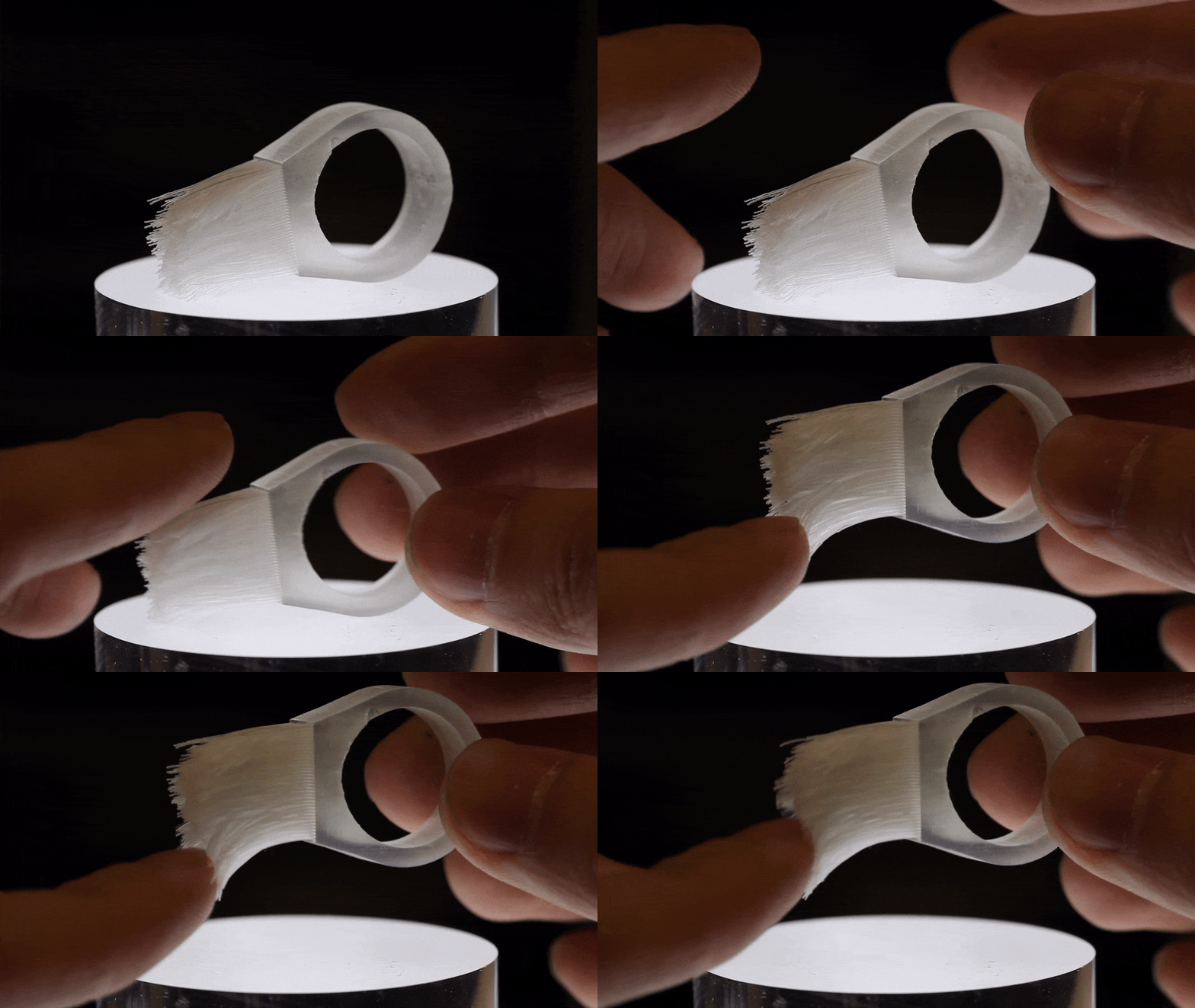
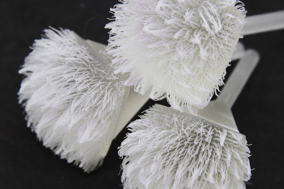
3-D printed hair (credit: Tangible Media Group/MIT Media Lab)

Researchers in MIT’s Media Lab have bypassed a major design step in 3-D printing — quickly and efficiently modeling and printing thousands of hair-like structures.

Instead of using conventional computer-aided design (CAD) software to draw thousands of individual hairs on a computer — a step that would take hours to compute — the team built a new software platform called “Cilllia” that lets users simply define the angle, thickness, density, and height of thousands of hairs in just a few minutes.

Using the new software, the researchers designed arrays of hair-like structures at a resolution of 50 micrometers — about the width of an average human hair. They then designed and printed arrays, ranging from coarse bristles to fine fur, onto flat and also curved surfaces, using a conventional 3-D printer.

The goal was to perform useful tasks such as sensing, adhesion, and actuation … and maybe create a few toys.

The 3-D printed hairs act like Velcro. (credit: MIT Media Lab researchers)

To demonstrate adhesion, the team printed arrays that act as Velcro-like bristle pads. Depending on the angle of the bristles, the pads can stick to each other with varying forces. For sensing, the researchers printed a small furry rabbit figure, equipped with LED lights that light up when a person strokes the rabbit in certain directions.

Vibrations cause a piece of metal to move across the 3-D printed hairs. (credit: MIT Media Lab researchers)

And to see whether 3-D-printed hair can help actuate, or move objects, the team fabricated a weight-sorting table made from panels of printed hair with specified angles and heights. As a small vibration source shook the panels, the hairs were able to move coins across the table,  sorting them based on the coins’ weight and the vibration frequency.

A software challenge

“[Hair] comes with a challenge that is not on the hardware, but on the software side,” says Jifei Ou, lead author on a paper presented at the Association for Computing Machinery’s CHI Conference on Human Factors in Computing Systems in May.

To 3-D-print hair using existing software, designers would have to model hair in CAD, drawing out each individual strand, then feed the drawing through a slicer program that represents each hair’s contour as a mesh of tiny triangles. The program would then create horizontal cross sections of the triangle mesh, and translate each cross section into pixels, or a bitmap, that a printer could then print out, layer by layer.

Ou says designing a stamp-sized array of 6,000 hairs using this process would take several hours to process. “If you were to load this file into a normal slicing program, it would crash the program,” he says.

Hair pixels

To design hair, the researchers chose to do away with CAD modeling entirely. Instead, they built a new software platform to model first a single hair and then an array of hairs, and finally to print arrays on both flat and curved surfaces.*

Using these techniques, the team printed pads of Velcro-like bristles, and paintbrushes with varying textures and densities.

The researchers attached the 3-D printed hairs to a ring. (credit: MIT Media Lab researchers)

Printing hair on curved surfaces proved trickier. To do this, the team first imported a CAD drawing of a curved surface, such as a small rabbit, then fed the model through a slicing program to generate a triangle mesh of the rabbit shape. They then developed an algorithm to locate the center of each triangle’s base, then virtually drew a line out, perpendicular to the triangle’s base, to represent a single hair. Doing this for every triangle in the mesh created a dense array of hairs running perpendicular to the rabbit’s curved surface.

The researchers then used their color mapping techniques to quickly customize the rabbit hair’s thickness and stiffness.

Interactive toys and other objects

“With our method, everything becomes smooth and fast,” Ou says. “Previously it was virtually impossible, because who’s going to take a whole day to render a whole furry rabbit, and then take another day to make it printable?”

Among other applications, Ou says 3-D-printed hair may be used in interactive toys. To demonstrate, his team inserted an LED light into the fuzzy printed rabbit, along with a small microphone that senses vibrations. With this setup, the bunny turns green when it is petted in the correct way, and red when it is not.

“The ability to fabricate customized hair-like structures not only expands the library of 3-D-printable shapes, but also enables us to design alternative actuators and sensors,” the authors conclude in their paper. “3-D-printed hair can be used for designing everyday interactive objects.”

Kelly Schaefer, a designer at IDEO, a design consulting firm, says “this type of work expands the possibilities of 3-D printing as an industry because of the new applications it suggests.”

* The researchers modeled a single hair by representing an elongated cone as a stack of fewer and fewer pixels, from the base to the top. To change the hair’s dimensions, such as its height, angle, and width, they simply changed the arrangement of pixels in the cone.

To scale up to thousands of hairs on a flat surface, Ou and his team used Photoshop to generate a color mapping technique. They used three colors — red, green, and blue — to represent three hair parameters — height, width, and angle. For example, to make a circular patch of hair with taller strands around the rim, they drew a red circle and changed the color gradient in such a way that darker hues of red appeared around the circle’s rim, denoting taller hairs. They then developed an algorithm to quickly translate the color map into a model of a hair array, which they then fed to a 3-D printer.


Abstract of Cilllia: 3D Printed Micro-Pillar Structures for Surface Texture, Actuation and Sensing

This work presents a method for 3D printing hair-like structures on both flat and curved surfaces. It allows a user to design and fabricate hair geometries that are smaller than 100 micron. We built a software platform to let users quickly define the hair angle, thickness, density, and height. The ability to fabricate customized hair-like structures not only expands the library of 3D-printable shapes, but also enables us to design passive actuators and swipe sensors. We also present several applications that show how the 3D-printed hair can be used for designing everyday interactive objects.

Ultra-flexible solar cells thin enough to wrap around a glass stirring rod

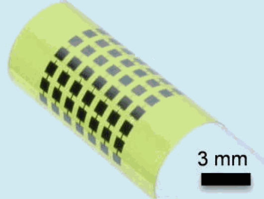
Ultra-thin solar cells flexible enough to bend around small objects, such as this 6-mm-diameter glass rod (credit: Juho Kim, et al./APL)

Scientists in South Korea have designed ultra-thin photovoltaics that are flexible enough to wrap around a thin glass rod. The new solar cells could power wearable electronics like smart watches and fitness trackers.

“Our photovoltaic is about 1 micrometer thick” (the thinnest human hair is about 17 micrometers), said Jongho Lee, an engineer at the Gwangju Institute of Science and Technology in South Korea. Standard photovoltaics are usually hundreds of times thicker, and most other thin photovoltaics are 2 to 4 times thicker, he explained.

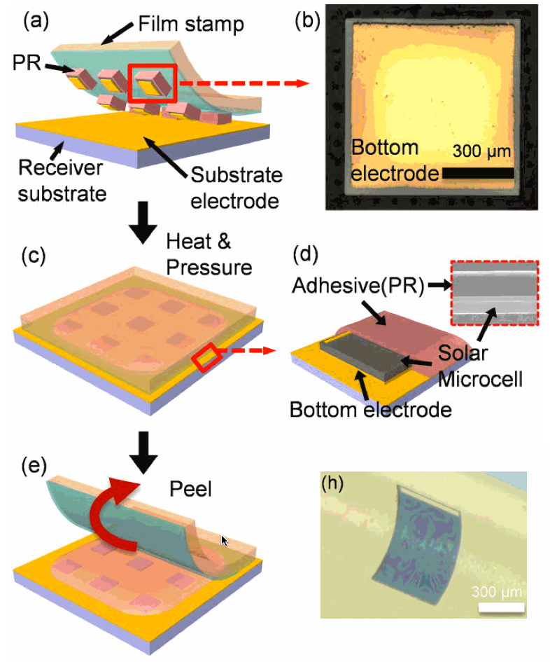
Fabrication procedure of the flexible vertical ultra-thin gallium-arsenide solar microcells.* (credit: Juho Kim, et al./APL)

The researchers made the ultra-thin solar cells from the semiconductor gallium arsenide. They stamped the cells directly onto a flexible substrate without using an adhesive (which would add to the material’s thickness).

The cells were then “cold welded” to the electrode on the substrate by applying pressure at 170 degrees Celsius and melting a top layer of material called photoresist, which acted as a temporary adhesive. The photoresist was later peeled away, leaving the direct metal-to-metal bond.

The metal bottom electrode layer also serves as a reflector to direct stray light back to the solar cells (to increase current output). The researchers tested the efficiency of the device at converting sunlight to electricity and found that it was comparable to thicker photovoltaics.

The team performed bending tests and found the cells could wrap around a radius as small as 1.4 millimeters. They also performed numerical analysis of the cells, finding that they experience one-fourth the amount of strain of similar cells that are 3.5 micrometers thick.

A few other groups have reported solar cells with thicknesses of around 1 micrometer, but have produced the cells in different ways, for example, by removing the whole subtrate by etching. By transfer-printing instead of etching, the new method developed by Lee and his colleagues could be used to make very flexible photovoltaics with a smaller amount of materials, according to Lee.

The thin cells can also be integrated onto glasses frames or fabric and might power the next wave of wearable electronics, Lee said.

The researchers report the results in an open-access paper in the journal Applied Physics Letters, from AIP Publishing.

* (a) Schematic illustration of a film stamp with vertical gallium-arsenide microcells fabricated and isolated from the epitaxially grown source wafers. The photoresist (PR) temporarily holds the solar microcells on the source wafers. (b) The bottom electrode, which also serves as a back reflector, is deposited onto the backside of the ultra-thin vertical GaAs microcells. (c) After the film stamp is brought into contact with the receiver substrate, heat (∼170 °C) and pressure (∼80 kPa) are applied to melt the PR to serve as an adhesive. (d) Cross-sectional scanning electron microscope (SEM) image of the microcell covered with the adhesive (PR) on the receiver substrate after the printing process. The bottom electrode is in direct contact with the Au layer on the receiver substrate. (e) Peeling the film stamp leaves the vertical ultra-thin solar microcells on the receiver substrate. (h) An optical image of the microcell wrapped on a glass slide with a radius of 1 mm. The microcell is encapsulated with a thin epoxy layer (thickness ∼2 μm).

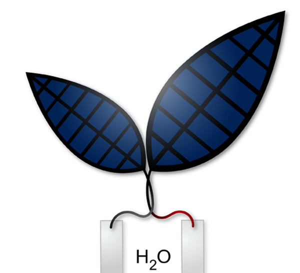
Bionic leaf 2.0

Bionic leaf 2.0: An artificial photosynthesis system (credit: Jessica Polka)

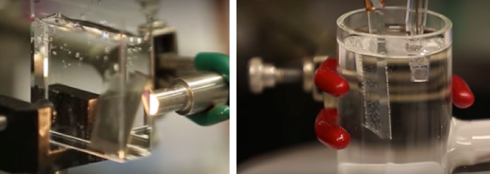
Harvard scientists have created a system a system that uses solar energy plus hydrogen-eating bacteria to produce liquid fuels with 10 percent efficiency, compared to the 1 percent seen in the fastest-growing plants.

The system, co-created by Daniel Nocera, the Patterson Rockwood Professor of Energy at Harvard University, and Pamela Silver, the Elliott T. and Onie H. Adams Professor of Biochemistry and Systems Biology at Harvard Medical School, uses solar energy to split water molecules into hydrogen and oxygen molecules.

A paper on the research was published June 3 in Science.

“This is a true artificial photosynthesis system,” Nocera said. “Before, people were using artificial photosynthesis for water-splitting, but this is a true A-to-Z system, and we’ve gone well over the efficiency of photosynthesis in nature.”

“What we’ve invented is an artificial leaf. You just drop it in water and sunlight hits it, and out one side comes hydrogen and out the other side comes oxygen.” — Daniel Nocera

“The beauty of biology is it’s the world’s greatest chemist: Biology can do chemistry we can’t do easily,” said Silver, who is also a founding core member of the Wyss Institute at Harvard University. “In principle, we have a platform that can make any downstream carbon-based molecule. So this has the potential to be incredibly versatile.”

Dubbed “bionic leaf 2.0,” the new system builds on previous work by Nocera, Silver and others, which faced a number of challenges. Mainly, the catalyst they used to produce hydrogen (a nickel-molybdenum-zinc alloy) also created reactive oxygen species — molecules that attacked and destroyed the bacteria’s DNA. To avoid that problem, researchers were forced to run the system at abnormally high voltages, resulting in reduced efficiency.

Ready for commercial applications, with a new model

“For this paper, we designed a new cobalt-phosphorus alloy catalyst, which we showed does not make reactive oxygen species,” Nocera said. “That allowed us to lower the voltage, and that led to a dramatic increase in efficiency.”

Nocera and colleagues were also able to expand the portfolio of the system to include isobutanol (a solvent) and isopentanol (used in geothermal power production to drive turbines), along with PHB, a bioplastic precursor.

“Instead of having a gas station, the Sun is hitting your house, you have the artificial leaf, you could be generating your own fuel.” — Daniel Nocera (credit: Rose Lincoln/Harvard Staff Photographer)

The new catalyst’s chemical design also allows it to “self-heal,” meaning it won’t leach material into solution — it’s biologically compatible.

Nocera said the system is already effective enough to consider possible commercial applications but within a different model for technology translation. “It’s an important discovery… [that] can do better than photosynthesis,” Nocera said. “But I also want to bring this technology to the developing world.”

Working in conjunction with the First 100 Watts Project at Harvard, which helped fund the research, Nocera hopes to continue developing the technology and its applications in nations such as India with the help of that country’s scientists.

In many ways, Nocera said, the new system marks fulfillment of the promise of his “artificial leaf,” which used solar power to split water and make hydrogen fuel (see ‘Artificial leaf’ harnesses sunlight for efficient, safe hydrogen fuel production).

“If you think about it, photosynthesis is amazing,” he said. “It takes sunlight, water and air—and then look at a tree. That’s exactly what we did, but we do it significantly better, because we turn all that energy into a fuel.”

The work, a direct result of the First 100 Watts Project established at Harvard University, was was supported by Office of Naval Research Multidisciplinary University, Research Initiative Award, Air Force Office of Scientific Research Grant, and the Wyss Institute for Biologically Inspired Engineering. The Harvard University Climate Change Solutions Fund is supporting ongoing research into the “bionic leaf” platform.


Harvard University | Bionic Leaf Turns Sunlight Into Liquid Fuel


Abstract of Water splitting–biosynthetic system with CO2 reduction efficiencies exceeding photosynthesis

Artificial photosynthetic systems can store solar energy and chemically reduce CO2. We developed a hybrid water splitting–biosynthetic system based on a biocompatible Earth-abundant inorganic catalyst system to split water into molecular hydrogen and oxygen (H2 and O2) at low driving voltages. When grown in contact with these catalysts, Ralstonia eutropha consumed the produced H2 to synthesize biomass and fuels or chemical products from low CO2 concentration in the presence of O2. This scalable system has a CO2 reduction energy efficiency of ~50% when producing bacterial biomass and liquid fusel alcohols, scrubbing 180 grams of CO2 per kilowatt-hour of electricity. Coupling this hybrid device to existing photovoltaic systems would yield a CO2 reduction energy efficiency of ~10%, exceeding that of natural photosynthetic systems.

Built-in miniaturized micro-supercapacitor powers silicon chip

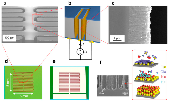
In-chip porous silicon-titanium nitride supercapacitor. (a) Scanning electron microscopy (SEM) inset of the trenches separating the electrodes (dark gray). (b) Rotated schematic illustration of the cross-section of two opposite electrodes of a device (titanium nitride-coated porous silicon layer with aluminum contact pads on the back side), with electrolyte shown in orange. (c) Higher-magnification SEM picture of the porous silicon regions. (d) Device trench side. (e) metallization side containing aluminum contacts for electrodes. (f) 3D illustration of two atomic-layer-deposition cycles of titanium-nitride growth. (credit: adapted from Kestutis Grigoras et al./Nano Energy)

Finnish researchers have developed a method for building highly efficient miniaturized micro-supercapacitor energy storage directly inside a silicon microcircuit chip, making it possible to power autonomous sensor networks, wearable electronics, and mobile internet-of-things (IoT) devices.

Supercapacitors function similar to standard batteries, but store electrostatic energy instead of chemical energy.

The researchers at VTT Technical Research Centre of Finland have developed a hybrid nano-electrode that’s only a few nanometers thick. It consists of porous silicon coated with a titanium nitride layer formed by atomic layer deposition.

The nano-electrode design features the highest-ever conductive surface-to-volume ratio. That combined with an ionic liquid (in a microchannel formed in between two electrodes), results in an extremely small form factor and efficient energy storage. That design makes it possible for a silicon-based micro-supercapacitor to achieve higher energy storage (energy density) and faster charge/discharge (power density) than the leading carbon- and graphene-based supercapacitors, according to the researchers.

The micro-supercapacitor can store 0.2 joule (55 microwatts of power for one hour) on a one-square-centimeter silicon chip. This design also leaves the surface of the chip available for active integrated microcircuits and sensors.

Micro-supercapacitors can also be integrated directly with active microelectronic devices to store electrical energy generated by thermal, light, and vibration energy harvesters to supply electrical energy (see, for example, Wireless device converts ‘lost’ microwave energy into electric power).

An open-access paper on the research has been published in Nano Energy journal.


Abstract of Conformal titanium nitride in a porous silicon matrix: A nanomaterial for in-chip supercapacitors

Today’s supercapacitor energy storages are typically discrete devices aimed for printed boards and power applications. The development of autonomous sensor networks and wearable electronics and the miniaturization of mobile devices would benefit substantially from solutions in which the energy storage is integrated with the active device. Nanostructures based on porous silicon (PS) provide a route towards integration due to the very high inherent surface area to volume ratio and compatibility with microelectronics fabrication processes. Unfortunately, pristine PS has limited wettability and poor chemical stability in electrolytes and the high resistance of the PS matrix severely limits the power efficiency. In this work, we demonstrate that excellent wettability and electro-chemical properties in aqueous and organic electrolytes can be obtained by coating the PS matrix with an ultra-thin layer of titanium nitride by atomic layer deposition. Our approach leads to very high specific capacitance (15 F cm−3), energy density (1.3 mWh cm−3), power density (up to 214 W cm−3) and excellent stability (more than 13,000 cycles). Furthermore, we show that the PS–TiN nanomaterial can be integrated inside a silicon chip monolithically by combining MEMS and nanofabrication techniques. This leads to realization of in-chip supercapacitor, i.e., it opens a new way to exploit the otherwise inactive volume of a silicon chip to store energy.

How creating defective nanodiamonds could revolutionize nanotechnology and quantum computing

This electron microscope image shows a hybrid nanoparticle consisting of a nanodiamond (roughly 50 nanometers wide) covered in smaller silver nanoparticles that enhance the diamond’s optical properties. (credit: Min Ouyang)

University of Maryland researchers have developed a method to quickly and inexpensively assemble diamond-based hybrid nanoparticles from the ground up in large quantities while avoiding many of the problems with current methods.

These hybrid nanoparticles could speed the design of room-temperature qubits for quantum computers and create brighter dyes for biomedical imaging or highly sensitive magnetic and temperature sensors, for example.

When impurities are better

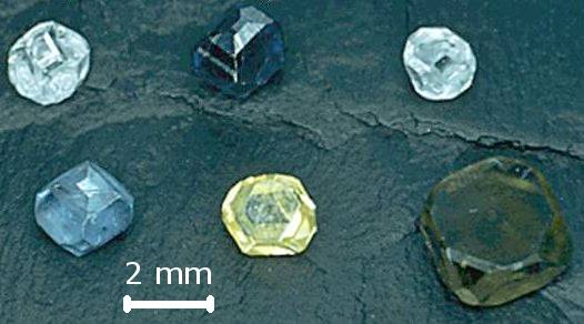
Synthetic diamonds of various colors (from defects) grown by the high-pressure high-temperature technique (credit: Wikipedia/
public domain)

The basic trick in creating a interesting or useful diamond is, ironically: Add a defect in the diamond’s crystal lattice. It’s similar to doping silicon to give it special electronic properties (such as making it work as a transistor).

Pure diamonds consist of an orderly lattice of carbon atoms and are completely transparent. However, pure diamonds are quite rare in natural diamond deposits; most have defects resulting from non-carbon impurities such as nitrogen, boron and phosphorus. Such defects create the subtle and desirable color variations seen in gemstone diamonds.

This altered bond is also the source of the optical, electromagnetic, and quantum physical properties that will make a nanodiamond useful when paired with other nanomaterials.

Nitrogen vacancy impurity

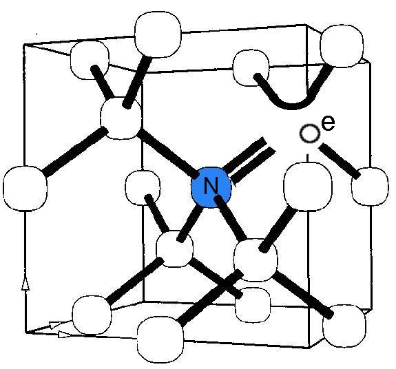
Model of nitrogen-vacancy center in diamond (credit: Wikipedia/public domain)

The most useful impurity — and used in the Maryland study — is the famous “nitrogen vacancy” defect: Sticking in a single nitrogen atom where a carbon atom should be, with an empty space right next to it.

As KurzweilAI has shown in several articles, a nitrogen vacancy in a diamond (or other crystalline materials) can lead to a variety of interesting new properties, such as a highly sensitive way to detect neural signals, an ultrasensitive real-time magnetic field detector, and importantly, making a nanodiamond behave as a quantum bit (qubit) for use in quantum computing and other applications.

Nearly all qubits studied to date require ultra-cold temperatures to function properly. A qubit that works at room temperature would represent a significant step forward, helping use quantum circuits in industrial, commercial and consumer-level electronics. That’s of special interest to Ougang’s team.

Volume production of hybrid nanoparticles

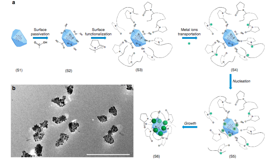
A synthetic route for hybrid nanodiamond nanoparticles. (a) Different growth stages, ending in (S6) growth of metal nanoparticles on the nanodiamond surface. (b) Transmission electron microscope image showing hybrid nanodiamond-silver nanostructures made by following the synthetic scheme in (a). Scale bar, 200 nm. (credit: J. Gong et al./Nature Communications)

Ougang’s and colleagues’ main breakthrough, though, is their method for constructing the hybrid nanoparticles. Other researchers have paired nanodiamonds with complementary nanoparticles using relatively imprecise methods, such as manually installing the diamonds and particles next to each other onto a larger surface one by one.

These top-down methods are costly, time consuming, and introduce a host of complications. “Our key innovation is that we can now reliably and efficiently produce these freestanding hybrid particles in large numbers,” explained Ouyang, who also has appointments in the UMD Center for Nanophysics and Advanced Materials and the Maryland NanoCenter, with an affiliate professorship in the UMD Department of Materials Science and Engineering.

His team’s method also enables precise control of the hybrid particles’ properties, such as the composition and total number of non-diamond particles.

“A major strength of our technique is that it is broadly useful and can be applied to a variety of diamond types and paired with a variety of other nanomaterials,” Ouyang said. “It can also be scaled up fairly easily. We are interested in studying the basic physics further, but also moving toward specific applications.”


Abstract of Nanodiamond-based nanostructures for coupling nitrogen-vacancy centres to metal nanoparticles and semiconductor quantum dots

The ability to control the interaction between nitrogen-vacancy centres in diamond and photonic and/or broadband plasmonic nanostructures is crucial for the development of solid-state quantum devices with optimum performance. However, existing methods typically employ top-down fabrication, which restrict scalable and feasible manipulation of nitrogen-vacancy centres. Here, we develop a general bottom-up approach to fabricate an emerging class of freestanding nanodiamond-based hybrid nanostructures with external functional units of either plasmonic nanoparticles or excitonic quantum dots. Precise control of the structural parameters (including size, composition, coverage and spacing of the external functional units) is achieved, representing a pre-requisite for exploring the underlying physics. Fine tuning of the emission characteristics through structural regulation is demonstrated by performing single-particle optical studies. This study opens a rich toolbox to tailor properties of quantum emitters, which can facilitate design guidelines for devices based on nitrogen-vacancy centres that use these freestanding hybrid nanostructures as building blocks.

‘On-the-fly’ 3-D printing system prints what you design, as you design it

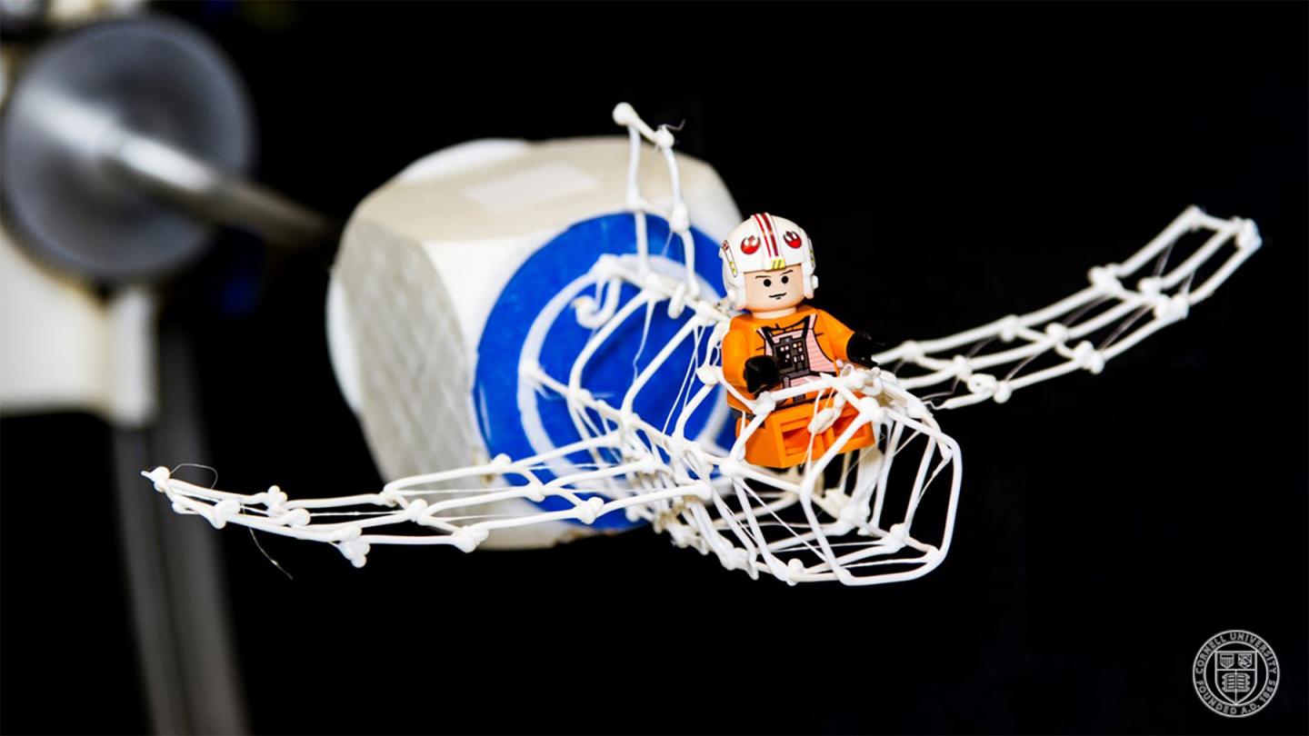
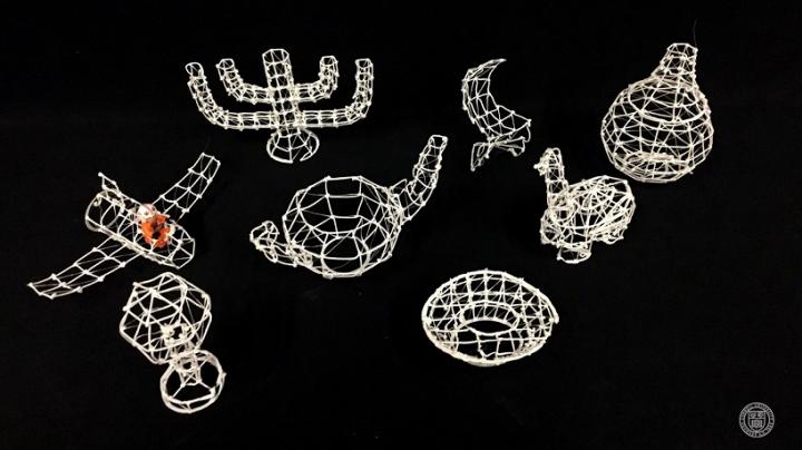
This wire frame prototype of a toy aircraft was printed in just 10 minutes, including testing for correct fit, and modified during printing to create the cockpit. The file was updated in the process, and could be used to print a finished model. (credit: Cornell University)

Cornell researchers have developed an interactive prototyping system that prints a wire frame of your design as you design it. You can pause anywhere in the process to test or measure and make needed changes, which will be added to the physical model still in the printer.

In conventional 3-D printing, a nozzle scans across a stage depositing drops of plastic, rising slightly after each pass to build an object in a series of layers. With the On-the-Fly-Print system, the nozzle instead extrudes a rope of quick-hardening plastic to create a wire frame that represents the surface of the solid object described in a computer-aided design (CAD) file and allows the designer to make refinements while printing is in progress.

Wireframe test models printed with On-The-Fly Print system (credit: Cornell University)

The printer’s stage can be rotated to present any face of the model facing up; so an airplane fuselage, for example, can be turned on its side to add a wing. There is also a cutter to remove parts of the model, say, to give the airplane a cockpit, and the nozzle can reach through the wire mesh to make changes inside. The system also adds yaw and pitch for five degrees of freedom.

The researchers described the On-the-Fly-Print system in a paper presented at the 2016 ACM Conference for Human Computer Interaction. The work was supported in part by the National Science Foundation and by Autodesk Corp.


Huaishu Peng | On-the-Fly Print: Incremental Printing While Modelling

Automated top-down design technique simplifies creation of DNA origami nanostructures

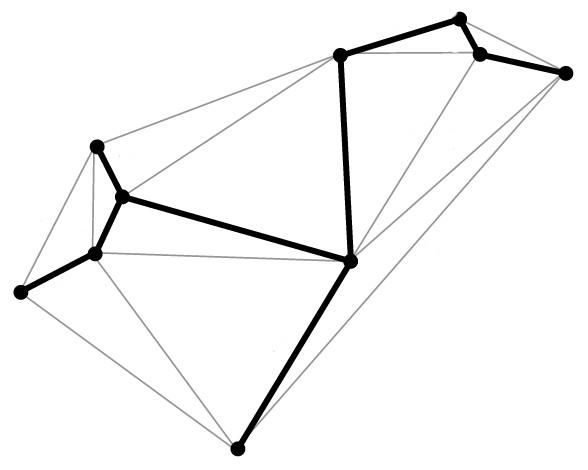
The boldfaced line, known as a spanning tree, follows the desired geometric shape of the target DNA origami design method, touching each vertex just once. A spanning tree algorithm is used to map out the proper routing path for the DNA strand. (credit: Public Domain)

MIT, Baylor College of Medicine, and Arizona State University Biodesign Institute researchers have developed a radical new top-down DNA origami* design method based on a computer algorithm that allows for creating designs for DNA nanostructures by simply inputting a target shape.

DNA origami (using DNA to design and build geometric structures) has already proven wildly successful in creating myriad forms in 2- and 3- dimensions, which conveniently self-assemble when the designed DNA sequences are mixed together. The tricky part is preparing the proper DNA sequence and routing design for scaffolding and staple strands to achieve the desired target structure. Typically, this is painstaking work that must be carried out manually.

The new algorithm, which is reported together with a novel synthesis approach in the journal Science, promises to eliminate all that and expands the range of possible applications of DNA origami in biomolecular science and nanotechnology. Think nanoparticles for drug delivery and cell targeting, nanoscale robots in medicine and industry, custom-tailored optical devices, and most interesting: DNA as a storage medium, offering retention times in the millions of years.**

Shape-shifting, top-down software

Unlike traditional DNA origami, in which the structure is built up manually by hand, the team’s radical top-down autonomous design method begins with an outline of the desired form and works backward in stages to define the required DNA sequence that will properly fold to form the finished product.

“The Science paper turns the problem around from one in which an expert designs the DNA needed to synthesize the object, to one in which the object itself is the starting point, with the DNA sequences that are needed automatically defined by the algorithm,” said Mark Bathe, an associate professor of biological engineering at MIT, who led the research. “Our hope is that this automation significantly broadens participation of others in the use of this powerful molecular design paradigm.”

The algorithm, which is known as DAEDALUS (DNA Origami Sequence Design Algorithm for User-defined Structures) after the Greek craftsman and artist who designed labyrinths that resemble origami’s complex scaffold structures, can build any type of 3-D shape, provided it has a closed surface. This can include shapes with one or more holes, such as a torus.

A simplified version of the  top-down procedure used to design scaffolded DNA origami nanostructures. It starts with a polygon corresponding to the target shape. Software translates a wireframe version of this structure into a plan for routing DNA scaffold and staple strands. That enables a 3D DNA-based atomic-level structural model that is then validated using 3D cryo-EM reconstruction. (credit: adapted from Biodesign Institute images)

With the new technique, the target geometric structure is first described in terms of a wire mesh made up of polyhedra, with a network of nodes and edges. A DNA scaffold using strands of custom length and sequence is generated, using a “spanning tree” algorithm — basically a map that will automatically guide the routing of the DNA scaffold strand through the entire origami structure, touching each vertex in the geometric form once. Complementary staple strands are then assigned and the final DNA structural model or nanoparticle self-assembles, and is then validated using 3D cryo-EM reconstruction.

The software allows for fabricating a variety of geometric DNA objects, including 35 polyhedral forms (Platonic, Archimedean, Johnson and Catalan solids), six asymmetric structures, and four polyhedra with nonspherical topology, using inverse design principles — no manual base-pair designs needed.

To test the method, simpler forms known as Platonic solids were first fabricated, followed by increasingly complex structures. These included objects with nonspherical topologies and unusual internal details, which had never been experimentally realized before. Further experiments confirmed that the DNA structures produced were potentially suitable for biological applications since they displayed long-term stability in serum and low-salt conditions.

Biological research uses

The research also paves the way for designing nanoscale systems mimicking the properties of viruses, photosynthetic organisms, and other sophisticated products of natural evolution. One such application is a scaffold for viral peptides and proteins for use as vaccines. The surface of the nanoparticles could be designed with any combination of peptides and proteins, located at any desired location on the structure, in order to mimic the way in which a virus appears to the body’s immune system.

The researchers demonstrated that the DNA nanoparticles are stable for more than six hours in serum, and are now attempting to increase their stability further.

The nanoparticles could also be used to encapsulate the CRISPR-Cas9 gene editing tool. The CRISPR-Cas9 tool has enormous potential in therapeutics, thanks to its ability to edit targeted genes. However, there is a significant need to develop techniques to package the tool and deliver it to specific cells within the body, Bathe says.

This is currently done using viruses, but these are limited in the size of package they can carry, restricting their use. The DNA nanoparticles, in contrast, are capable of carrying much larger gene packages and can easily be equipped with molecules that help target the right cells or tissue.

The most exciting aspect of the work, however, is that it should significantly broaden participation in the application of this technology, Bathe says, much like 3-D printing has done for complex 3-D geometric models at the macroscopic scale.

Hao Yan directs the Biodesign Center for Molecular Design and Biomimetics at Arizona State University and is the Milton D. Glick Distinguished Professor, College of Liberal Arts and Sciences, School of Molecular Sciences at ASU.

* DNA origami brings the ancient Japanese method of paper folding down to the molecular scale. The basics are simple: Take a length of single-stranded DNA and guide it into a desired shape, fastening the structure together using shorter “staple strands,” which bind in strategic places along the longer length of DNA. The method relies on the fact that DNA’s four nucleotide letters—A, T, C, & G stick together in a consistent manner — As always pairing with Ts and Cs with Gs.

The DNA molecule in its characteristic double stranded form is fairly stiff, compared with single-stranded DNA, which is flexible. For this reason, single stranded DNA makes for an ideal lace-like scaffold material. Further, its pairing properties are predictable and consistent (unlike RNA).

** A single gram of DNA can store about 700 terabytes of information — an amount equivalent to 14,000 50-gigabyte Blu-ray disks — and could potentially be operated with a fraction of the energy required for other information storage options.


Biodesign Institute at ASU | DNA Origami


Abstract of Designer nanoscale DNA assemblies programmed from the top down

Scaffolded DNA origami is a versatile means of synthesizing complex molecular architectures. However, the approach is limited by the need to forward-design specific Watson-Crick base-pairing manually for any given target structure. Here, we report a general, top-down strategy to design nearly arbitrary DNA architectures autonomously based only on target shape. Objects are represented as closed surfaces rendered as polyhedral networks of parallel DNA duplexes, which enables complete DNA scaffold routing with a spanning tree algorithm. The asymmetric polymerase chain reaction was applied to produce stable, monodisperse assemblies with custom scaffold length and sequence that are verified structurally in 3D to be high fidelity using single-particle cryo-electron microscopy. Their long-term stability in serum and low-salt buffer confirms their utility for biological as well as nonbiological applications.