Viewers of Quantum Events Are Also Subject to Uncertainty
New nanomaterial, quantum encryption system could be ultimate defenses against hackers

New physically unclonable nanomaterial (credit: Abdullah Alharbi et al./ACS Nano)
Recent advances in quantum computers may soon give hackers access to machines powerful enough to crack even the toughest of standard internet security codes. With these codes broken, all of our online data — from medical records to bank transactions — could be vulnerable to attack.
Now, a new low-cost nanomaterial developed by New York University Tandon School of Engineering researchers can be tuned to act as a secure authentication key to encrypt computer hardware and data. The layered molybdenum disulfide (MoS2) nanomaterial cannot be physically cloned (duplicated) — replacing programming, which can be hacked.
In a paper published in the journal ACS Nano, the researchers explain that the new nanomaterial has the highest possible level of structural randomness, making it physically unclonable. It achieves this with randomly occurring regions that alternately emit or do not emit light. When exposed to light, this pattern can be used to create a one-of-a-kind binary cryptographic authentication key that could secure hardware components at minimal cost.
The research team envisions a future in which similar nanomaterials can be inexpensively produced at scale and applied to a chip or other hardware component. “No metal contacts are required, and production could take place independently of the chip fabrication process,” according to Davood Shahrjerdi, Assistant Professor of Electrical and Computer Engineering. “It’s maximum security with minimal investment.”
The National Science Foundation and the U.S. Army Research Office supported the research.
A high-speed quantum encryption system to secure the future internet

Schematic of the experimental quantum key distribution setup (credit: Nurul T. Islam et al./Science Advances)
Another approach to the hacker threat is being developed by scientists at Duke University, The Ohio State University and Oak Ridge National Laboratory. It would use the properties that drive quantum computers to create theoretically hack-proof forms of quantum data encryption.
Called quantum key distribution (QKD), it takes advantage of one of the fundamental properties of quantum mechanics: Measuring tiny bits of matter like electrons or photons automatically changes their properties, which would immediately alert both parties to the existence of a security breach. However, current QKD systems can only transmit keys at relatively low rates — up to hundreds of kilobits per second — which are too slow for most practical uses on the internet.
The new experimental QKD system is capable of creating and distributing encryption codes at megabit-per-second rates — five to 10 times faster than existing methods and on a par with current internet speeds when running several systems in parallel. In an online open-access article in Science Advances, the researchers show that the technique is secure from common attacks, even in the face of equipment flaws that could open up leaks.
This research was supported by the Office of Naval Research, the Defense Advanced Research Projects Agency, and Oak Ridge National Laboratory.
Abstract of Physically Unclonable Cryptographic Primitives by Chemical Vapor Deposition of Layered MoS2
Physically unclonable cryptographic primitives are promising for securing the rapidly growing number of electronic devices. Here, we introduce physically unclonable primitives from layered molybdenum disulfide (MoS2) by leveraging the natural randomness of their island growth during chemical vapor deposition (CVD). We synthesize a MoS2 monolayer film covered with speckles of multilayer islands, where the growth process is engineered for an optimal speckle density. Using the Clark–Evans test, we confirm that the distribution of islands on the film exhibits complete spatial randomness, hence indicating the growth of multilayer speckles is a spatial Poisson process. Such a property is highly desirable for constructing unpredictable cryptographic primitives. The security primitive is an array of 2048 pixels fabricated from this film. The complex structure of the pixels makes the physical duplication of the array impossible (i.e., physically unclonable). A unique optical response is generated by applying an optical stimulus to the structure. The basis for this unique response is the dependence of the photoemission on the number of MoS2 layers, which by design is random throughout the film. Using a threshold value for the photoemission, we convert the optical response into binary cryptographic keys. We show that the proper selection of this threshold is crucial for maximizing combination randomness and that the optimal value of the threshold is linked directly to the growth process. This study reveals an opportunity for generating robust and versatile security primitives from layered transition metal dichalcogenides.
Abstract of Provably secure and high-rate quantum key distribution with time-bin qudits
The security of conventional cryptography systems is threatened in the forthcoming era of quantum computers. Quantum key distribution (QKD) features fundamentally proven security and offers a promising option for quantum-proof cryptography solution. Although prototype QKD systems over optical fiber have been demonstrated over the years, the key generation rates remain several orders of magnitude lower than current classical communication systems. In an effort toward a commercially viable QKD system with improved key generation rates, we developed a discrete-variable QKD system based on time-bin quantum photonic states that can generate provably secure cryptographic keys at megabit-per-second rates over metropolitan distances. We use high-dimensional quantum states that transmit more than one secret bit per received photon, alleviating detector saturation effects in the superconducting nanowire single-photon detectors used in our system that feature very high detection efficiency (of more than 70%) and low timing jitter (of less than 40 ps). Our system is constructed using commercial off-the-shelf components, and the adopted protocol can be readily extended to free-space quantum channels. The security analysis adopted to distill the keys ensures that the demonstrated protocol is robust against coherent attacks, finite-size effects, and a broad class of experimental imperfections identified in our system.
Math’s $1,000,000 Question Isn’t Just for Mathematicians Anymore

A Radical Vision of the Universe Returns to Electrify Physics

Berkeley Lab announces first transistor with a working 1-nanometer gate
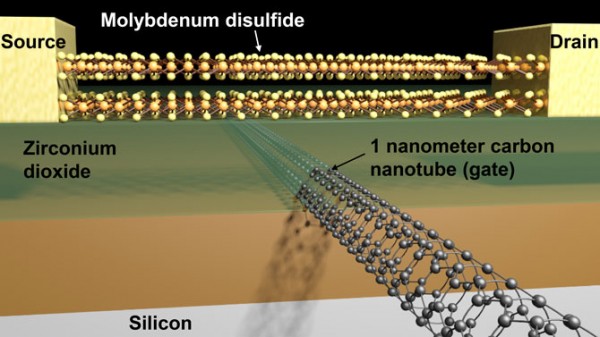
Schematic of a transistor with molybdenum disulfide semiconductor and 1-nanometer carbon nanotube gate. (credit: Sujay Desai/Berkeley Lab)
The first transistor with a working 1-nanometer (nm) gate* has been created by a team led by Lawrence Berkeley National Laboratory (Berkeley Lab) scientists. Until now, a transistor gate size less than 5 nanometers has been considered impossible because of quantum tunneling effects. (One nanometer is the diameter of a glucose molecule.)
The breakthrough was achieved by creating a 2D (flat) semiconductor field-effect transistor using molybdenum disulfide (MoS2) instead of silicon and a 1D single-walled carbon nanotube (SWCNT) as a gate electrode, instead of various metals. (SWCNTs are hollow cylindrical tubes with diameters as small as 1 nanometer.)
The MoS2 advantage
Compared with MoS2, electrons flowing through silicon are lighter and encounter less resistance . But with a gate length below 5 nanometers in length, a quantum mechanical phenomenon called tunneling kicks in, and the gate barrier is no longer able to keep the electrons from barging through from the source to the drain terminals, so the transistor cannot be turned off.
Electrons flowing through MoS2 are heavier, so their flow can be controlled with smaller gate lengths. MoS2 can also be scaled down to atomically thin sheets, about 0.65 nanometers thick, with a a larger band gap and lower dielectric constant, a measure reflecting the ability of a material to store energy in an electric field (similar to a capacitor). These properties help improve the control of the flow of current inside the transistor when the gate length is reduced to 1 nanometer.
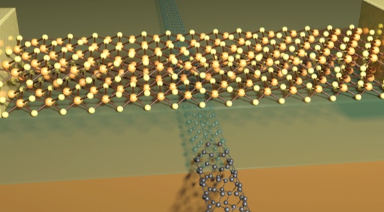
Transistors consist of three terminals: a source (left), a drain (right), and a gate (the carbon nanotube, black, below). Current flows through the semiconductor (MoS2, represented by the yellow molecular model) from the source to the drain. Based on the voltage applied to the gate, it switches the channel (the portion of the MoS2 semiconductor just above the carbon nanotube) on and off, via a dielectric (zirconium oxide, green), operating in a manner similar to a capacitor. (credit: Sujay Desai/Berkeley Lab)
“We made the smallest transistor reported to date,” said faculty scientist Ali Javey at the Department of Energy’s Lawrence Berkeley National Laboratory (Berkeley Lab) and lead principal investigator of the Electronic Materials program in Berkeley Lab’s Materials Science Division. “The gate length is considered a defining dimension of the transistor. We demonstrated a 1-nanometer-gate transistor, showing that with the choice of proper materials, there is a lot more room to shrink our electronics.”
The development could be key to keeping alive Intel co-founder Gordon Moore’s prediction that the density of transistors on integrated circuits would double every two years, enabling the increased performance of our laptops, mobile phones, televisions, and other electronics.
“The semiconductor industry has long assumed that any gate below 5 nanometers wouldn’t work, so anything below that was not even considered,” said study lead author Sujay Desai, a graduate student in Javey’s lab. “This research shows that sub-5-nanometer gates should not be discounted. Industry has been squeezing every last bit of capability out of silicon. By changing the material from silicon to MoS2, we can make a transistor with a gate that is just 1 nanometer in length, and operate it like a switch.”
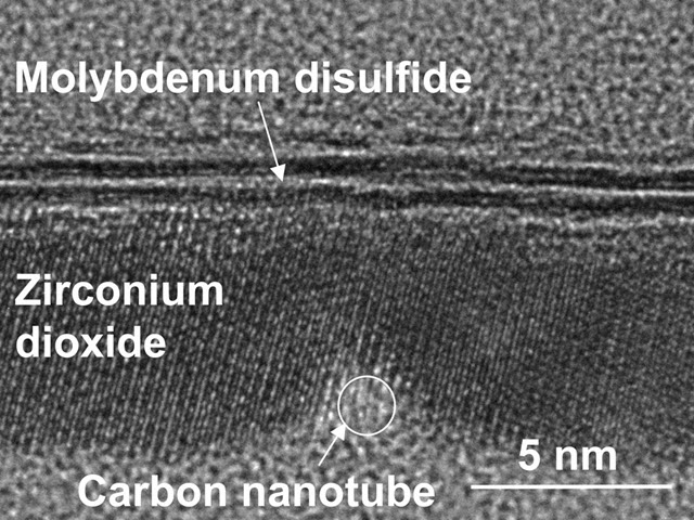
Transmission electron microscope image of a cross section of the transistor, showing the edge of a 1-nanometer carbon nanotube gate and the molybdenum disulfide semiconductor separated by zirconium dioxide, which is a dielectric insulator. (credit: Sujay B. Desai/Science)
Continuing Moore’s law
“This work demonstrated the shortest transistor ever,” said Javey, who is also a UC Berkeley professor of electrical engineering and computer sciences. “However, it’s a proof of concept. We have not yet packed these transistors onto a chip, and we haven’t done this billions of times over. We also have not developed self-aligned fabrication schemes for reducing parasitic resistances in the device. But this work is important to show that we are no longer limited to a 5-nanometer gate for our transistors. Moore’s Law can continue a while longer by proper engineering of the semiconductor material and device architecture.”
The findings appeared in the Oct. 7 issue of the journal Science. Researchers at the University of Texas at Dallas, Stanford University, and the University of California, Berkeley, were also involved. The work at Berkeley Lab was primarily funded by the Department of Energy’s Basic Energy Sciences program.
According to an earlier article in CTimes on Sept. 30, Taiwan Semiconductor Manufacturing Co., Ltd. (TSMC) said the company is working toward a 1-nanometer manufacturing process, starting with a “5 nanometers process technology, while putting about 300 to 400 R&D personnel in developing more advanced 3-nanometer process.” However, TSMC spokesperson Elizabeth Sun told KurzweilAI that “no further information regarding any technology either under development or in path-finding stage will be disclosed to the public at this point.”
* Gate length is the length of the gate portion of the transistor, not to be confused with “node,” which was initially a measure of “half pitch” (half of the distance between features of a transistor), but the number itself has lost the exact meaning it once held. Gate length was 26nm for the 22nm node from Intel and 20 nanometers for the more recent 14nm node from Intel. — S. Natarajan et al., “A 14nm logic technology featuring 2nd-generation FinFET, air-gapped interconnects, self-aligned double patterning and a 0.0588 µm2 SRAM cell size,” 2014 IEEE International Electron Devices Meeting, San Francisco, CA, 2014, pp. 3.7.1-3.7.3. doi: 10.1109/IEDM.2014.7046976
Abstract of MoS2 transistors with 1-nanometer gate lengths
Scaling of silicon (Si) transistors is predicted to fail below 5-nanometer (nm) gate lengths because of severe short channel effects. As an alternative to Si, certain layered semiconductors are attractive for their atomically uniform thickness down to a monolayer, lower dielectric constants, larger band gaps, and heavier carrier effective mass. Here, we demonstrate molybdenum disulfide (MoS2) transistors with a 1-nm physical gate length using a single-walled carbon nanotube as the gate electrode. These ultrashort devices exhibit excellent switching characteristics with near ideal subthreshold swing of ~65 millivolts per decade and an On/Off current ratio of ~106. Simulations show an effective channel length of ~3.9 nm in the Off state and ~1 nm in the On state.
D-Wave Systems previews 2000-qubit quantum processor

D-Wave 2000-qubit processor (credit: D-Wave Systems)
D-Wave Systems announced Tuesday (Sept. 28, 2016) a new 2000-qubit processor, doubling the number of qubits over the previous-generation D-Wave 2X system. The new system will enable larger problems to be solved and performance improvements of up to 1000 times.
D-Wave’s quantum system runs a quantum-annealing algorithm to find the lowest points in a virtual energy landscape representing a computational problem to be solved. The lowest points in the landscape correspond to optimal or near-optimal solutions to the problem. The increase in qubit count enables larger and more difficult problems to be solved, and the ability to tune the rate of annealing of individual qubits will enhance application performance.
According to D-Wave, users will be able to tune the quantum computational process to solve problems faster and find more diverse solutions when they exist. They will have the ability to sample the state of the quantum computer during the quantum annealing process, which will power hybrid quantum-classical machine learning algorithms that were not possible before.
The system will also allow for combining quantum processing with classical processing, improving the quality of optimization and sampling results returned from the system.
D-Wave’s first users conference, being held on September 28–29 in Santa Fe, New Mexico, features speakers from Los Alamos National Laboratory, NASA, Lockheed Martin, the Roswell Park Cancer Center, Oak Ridge National Laboratory, USC, and D-Wave, and a number of quantum software and services companies.
Google’s secret plan for quantum computer supremacy

UCSB Martinis Group’s superconducting five-qubit array (credit: Erik Lucero)
Google* is developing a quantum computer that it believes will outperform the world’s top supercomputers, according to an August 31 New Scientist article and sourced to researchers contacted by the magazine.
Google’s ambitious goal is to achieve “quantum supremacy”— which would be achieved when “quantum devices without error correction can perform a well-defined computational task beyond the capabilities of state-of-the-art classical computers,” as the authors of an arXiv paper (open access) explain.
The task in this case: simulate the behavior of a random arrangement of quantum circuits in a 48-qubit grid, which would require 2.252 petabytes of memory, almost double that of the top supercomputer in the world.
To do that, Google plans to build a whopping 50 qubit computer. So far, Google has only announced a modest nine qubit computer, but it has hired arXiv paper co-author John M. Martinis at the University of California, Santa Barbara (see “Google partners with UC Santa Barbara team to build new superconductor-based quantum information processors” on KurzweilAI) to try.
Success may prepare Google to construct something even bigger: a fully scalable machine,” says Ian Walmsley at the University of Oxford.
* With partners NASA Ames, SGT, and University of California, Santa Barbara
How creating defective nanodiamonds could revolutionize nanotechnology and quantum computing
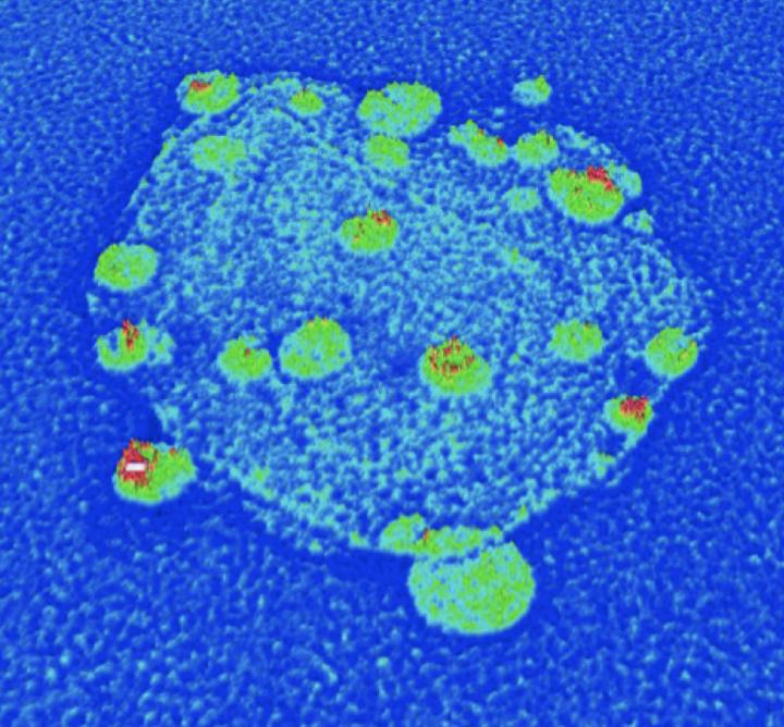
This electron microscope image shows a hybrid nanoparticle consisting of a nanodiamond (roughly 50 nanometers wide) covered in smaller silver nanoparticles that enhance the diamond’s optical properties. (credit: Min Ouyang)
University of Maryland researchers have developed a method to quickly and inexpensively assemble diamond-based hybrid nanoparticles from the ground up in large quantities while avoiding many of the problems with current methods.
These hybrid nanoparticles could speed the design of room-temperature qubits for quantum computers and create brighter dyes for biomedical imaging or highly sensitive magnetic and temperature sensors, for example.
When impurities are better
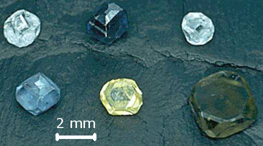
Synthetic diamonds of various colors (from defects) grown by the high-pressure high-temperature technique (credit: Wikipedia/
public domain)
The basic trick in creating a interesting or useful diamond is, ironically: Add a defect in the diamond’s crystal lattice. It’s similar to doping silicon to give it special electronic properties (such as making it work as a transistor).
Pure diamonds consist of an orderly lattice of carbon atoms and are completely transparent. However, pure diamonds are quite rare in natural diamond deposits; most have defects resulting from non-carbon impurities such as nitrogen, boron and phosphorus. Such defects create the subtle and desirable color variations seen in gemstone diamonds.
This altered bond is also the source of the optical, electromagnetic, and quantum physical properties that will make a nanodiamond useful when paired with other nanomaterials.
Nitrogen vacancy impurity
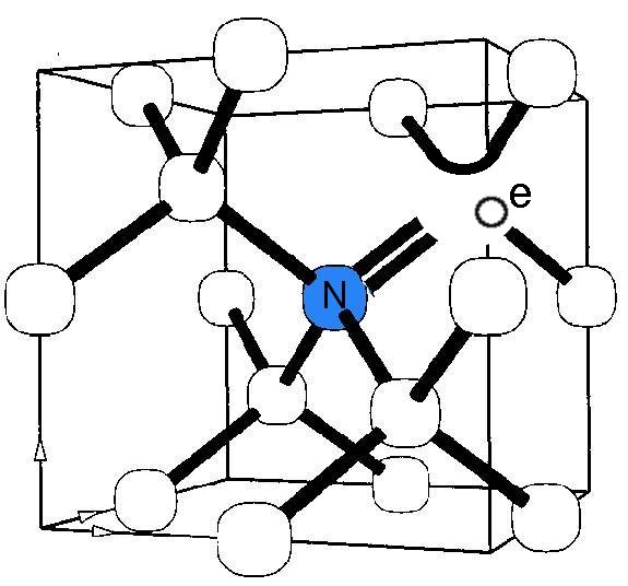
Model of nitrogen-vacancy center in diamond (credit: Wikipedia/public domain)
The most useful impurity — and used in the Maryland study — is the famous “nitrogen vacancy” defect: Sticking in a single nitrogen atom where a carbon atom should be, with an empty space right next to it.
As KurzweilAI has shown in several articles, a nitrogen vacancy in a diamond (or other crystalline materials) can lead to a variety of interesting new properties, such as a highly sensitive way to detect neural signals, an ultrasensitive real-time magnetic field detector, and importantly, making a nanodiamond behave as a quantum bit (qubit) for use in quantum computing and other applications.
Nearly all qubits studied to date require ultra-cold temperatures to function properly. A qubit that works at room temperature would represent a significant step forward, helping use quantum circuits in industrial, commercial and consumer-level electronics. That’s of special interest to Ougang’s team.
Volume production of hybrid nanoparticles
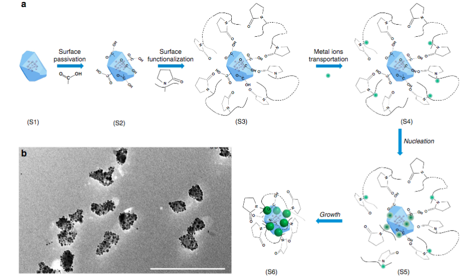
A synthetic route for hybrid nanodiamond nanoparticles. (a) Different growth stages, ending in (S6) growth of metal nanoparticles on the nanodiamond surface. (b) Transmission electron microscope image showing hybrid nanodiamond-silver nanostructures made by following the synthetic scheme in (a). Scale bar, 200 nm. (credit: J. Gong et al./Nature Communications)
Ougang’s and colleagues’ main breakthrough, though, is their method for constructing the hybrid nanoparticles. Other researchers have paired nanodiamonds with complementary nanoparticles using relatively imprecise methods, such as manually installing the diamonds and particles next to each other onto a larger surface one by one.
These top-down methods are costly, time consuming, and introduce a host of complications. “Our key innovation is that we can now reliably and efficiently produce these freestanding hybrid particles in large numbers,” explained Ouyang, who also has appointments in the UMD Center for Nanophysics and Advanced Materials and the Maryland NanoCenter, with an affiliate professorship in the UMD Department of Materials Science and Engineering.
His team’s method also enables precise control of the hybrid particles’ properties, such as the composition and total number of non-diamond particles.
“A major strength of our technique is that it is broadly useful and can be applied to a variety of diamond types and paired with a variety of other nanomaterials,” Ouyang said. “It can also be scaled up fairly easily. We are interested in studying the basic physics further, but also moving toward specific applications.”
Abstract of Nanodiamond-based nanostructures for coupling nitrogen-vacancy centres to metal nanoparticles and semiconductor quantum dots
The ability to control the interaction between nitrogen-vacancy centres in diamond and photonic and/or broadband plasmonic nanostructures is crucial for the development of solid-state quantum devices with optimum performance. However, existing methods typically employ top-down fabrication, which restrict scalable and feasible manipulation of nitrogen-vacancy centres. Here, we develop a general bottom-up approach to fabricate an emerging class of freestanding nanodiamond-based hybrid nanostructures with external functional units of either plasmonic nanoparticles or excitonic quantum dots. Precise control of the structural parameters (including size, composition, coverage and spacing of the external functional units) is achieved, representing a pre-requisite for exploring the underlying physics. Fine tuning of the emission characteristics through structural regulation is demonstrated by performing single-particle optical studies. This study opens a rich toolbox to tailor properties of quantum emitters, which can facilitate design guidelines for devices based on nitrogen-vacancy centres that use these freestanding hybrid nanostructures as building blocks.
Machine learning outperforms physicists in experiment
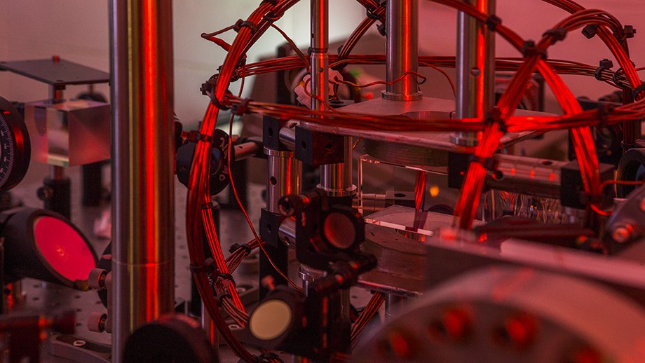
The experiment, featuring the small red glow of a BEC trapped in infrared laser beams (credit: Stuart Hay, ANU)
Australian physicists have used an online optimization process based on machine learning to produce effective Bose-Einstein condensates (BECs) in a fraction of the time it would normally take the researchers.
A BEC is a state of matter of a dilute gas of atoms trapped in a laser beam and cooled to temperatures just above absolute zero. BECs are extremely sensitive to external disturbances, which makes them ideal for research into quantum phenomena or for making very precise measurements such as tiny changes in the Earth’s magnetic field or gravity.
The experiment, developed by physicists from ANU, University of Adelaide and UNSW ADFA, demonstrated that “machine-learning online optimization” can discover optimized condensation methods “with less experiments than a competing optimization method and provide insight into which parameters are important in achieving condensation,” the physicists explain in an open-access paper in the Nature group journal Scientific Reports.
Faster, cheaper than a physicist
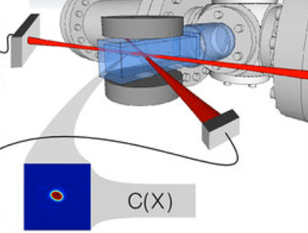
Optical dipole trap used in the experiment, showing the three laser beams and the condensate (red-yellow oval in blue square) (credit: P. B. Wigley et al./Scientific Reports)
The team cooled the gas to around 5 microkelvin. To further cool down the trapped gas (containing about 40 million rubidium atoms) to on the order of nanokelvin*, they then handed control of the three laser beams** over to the machine-learning program.
The physicists were surprised by the clever methods the system came up with to create a BEC, like changing one laser’s power up and down, and compensating with another laser.
“I didn’t expect the machine could learn to do the experiment itself, from scratch, in under an hour,” said co-lead researcher Paul Wigley from ANU Research School of Physics and Engineering. “A simple computer program would have taken longer than the age of the universe to run through all the combinations and work this out.”
Wigley suggested that one could make a working device to measure gravity that you could take in the back of a car, and the AI would automatically recalibrate and fix itself.
“It’s cheaper than taking a physicist everywhere with you,” he said.
* Billionth of a degree above absolute zero — where a phase transition occurs, and a macroscopic number of atoms start to occupy the same quantum state, called Bose-Einstein condensation.
** The 1064 nm beam is controlled by varying the current to the laser, while the 1090 nm beam is controlled using the current and a waveplate rotation stage combined with a polarizing beamsplitter to provide additional power attenuation while maintaining mode stability.
Abstract of Fast machine-learning online optimization of ultra-cold-atom experiments
We apply an online optimization process based on machine learning to the production of Bose-Einstein condensates (BEC). BEC is typically created with an exponential evaporation ramp that is optimal for ergodic dynamics with two-body s-wave interactions and no other loss rates, but likely sub-optimal for real experiments. Through repeated machine-controlled scientific experimentation and observations our ‘learner’ discovers an optimal evaporation ramp for BEC production. In contrast to previous work, our learner uses a Gaussian process to develop a statistical model of the relationship between the parameters it controls and the quality of the BEC produced. We demonstrate that the Gaussian process machine learner is able to discover a ramp that produces high quality BECs in 10 times fewer iterations than a previously used online optimization technique. Furthermore, we show the internal model developed can be used to determine which parameters are essential in BEC creation and which are unimportant, providing insight into the optimization process of the system.
